EP0249762A1 - Identifizierung von Halbleiterscheiben mit Mustern des "Bar-code"-Typs - Google Patents
Identifizierung von Halbleiterscheiben mit Mustern des "Bar-code"-Typs Download PDFInfo
- Publication number
- EP0249762A1 EP0249762A1 EP87107307A EP87107307A EP0249762A1 EP 0249762 A1 EP0249762 A1 EP 0249762A1 EP 87107307 A EP87107307 A EP 87107307A EP 87107307 A EP87107307 A EP 87107307A EP 0249762 A1 EP0249762 A1 EP 0249762A1
- Authority
- EP
- European Patent Office
- Prior art keywords
- bar code
- metal layer
- code pattern
- semiconductor wafer
- wafer
- Prior art date
- Legal status (The legal status is an assumption and is not a legal conclusion. Google has not performed a legal analysis and makes no representation as to the accuracy of the status listed.)
- Granted
Links
Images


Classifications
-
- H—ELECTRICITY
- H10—SEMICONDUCTOR DEVICES; ELECTRIC SOLID-STATE DEVICES NOT OTHERWISE PROVIDED FOR
- H10P—GENERIC PROCESSES OR APPARATUS FOR THE MANUFACTURE OR TREATMENT OF DEVICES COVERED BY CLASS H10
- H10P90/00—Preparation of wafers not covered by a single main group of this subclass, e.g. wafer reinforcement
- H10P90/12—Preparing bulk and homogeneous wafers
- H10P90/128—Preparing bulk and homogeneous wafers by edge treatment, e.g. chamfering
-
- H—ELECTRICITY
- H10—SEMICONDUCTOR DEVICES; ELECTRIC SOLID-STATE DEVICES NOT OTHERWISE PROVIDED FOR
- H10W—GENERIC PACKAGES, INTERCONNECTIONS, CONNECTORS OR OTHER CONSTRUCTIONAL DETAILS OF DEVICES COVERED BY CLASS H10
- H10W46/00—Marks applied to devices, e.g. for alignment or identification
-
- H—ELECTRICITY
- H10—SEMICONDUCTOR DEVICES; ELECTRIC SOLID-STATE DEVICES NOT OTHERWISE PROVIDED FOR
- H10P—GENERIC PROCESSES OR APPARATUS FOR THE MANUFACTURE OR TREATMENT OF DEVICES COVERED BY CLASS H10
- H10P72/00—Handling or holding of wafers, substrates or devices during manufacture or treatment thereof
- H10P72/06—Apparatus for monitoring, sorting, marking, testing or measuring
- H10P72/0614—Marking devices
-
- H—ELECTRICITY
- H10—SEMICONDUCTOR DEVICES; ELECTRIC SOLID-STATE DEVICES NOT OTHERWISE PROVIDED FOR
- H10P—GENERIC PROCESSES OR APPARATUS FOR THE MANUFACTURE OR TREATMENT OF DEVICES COVERED BY CLASS H10
- H10P72/00—Handling or holding of wafers, substrates or devices during manufacture or treatment thereof
- H10P72/06—Apparatus for monitoring, sorting, marking, testing or measuring
- H10P72/0618—Apparatus for monitoring, sorting, marking, testing or measuring using identification means, e.g. labels on substrates or labels on containers
-
- H—ELECTRICITY
- H10—SEMICONDUCTOR DEVICES; ELECTRIC SOLID-STATE DEVICES NOT OTHERWISE PROVIDED FOR
- H10W—GENERIC PACKAGES, INTERCONNECTIONS, CONNECTORS OR OTHER CONSTRUCTIONAL DETAILS OF DEVICES COVERED BY CLASS H10
- H10W46/00—Marks applied to devices, e.g. for alignment or identification
- H10W46/401—Marks applied to devices, e.g. for alignment or identification for identification or tracking
-
- H—ELECTRICITY
- H10—SEMICONDUCTOR DEVICES; ELECTRIC SOLID-STATE DEVICES NOT OTHERWISE PROVIDED FOR
- H10W—GENERIC PACKAGES, INTERCONNECTIONS, CONNECTORS OR OTHER CONSTRUCTIONAL DETAILS OF DEVICES COVERED BY CLASS H10
- H10W46/00—Marks applied to devices, e.g. for alignment or identification
- H10W46/501—Marks applied to devices, e.g. for alignment or identification for use before dicing
-
- Y—GENERAL TAGGING OF NEW TECHNOLOGICAL DEVELOPMENTS; GENERAL TAGGING OF CROSS-SECTIONAL TECHNOLOGIES SPANNING OVER SEVERAL SECTIONS OF THE IPC; TECHNICAL SUBJECTS COVERED BY FORMER USPC CROSS-REFERENCE ART COLLECTIONS [XRACs] AND DIGESTS
- Y10—TECHNICAL SUBJECTS COVERED BY FORMER USPC
- Y10S—TECHNICAL SUBJECTS COVERED BY FORMER USPC CROSS-REFERENCE ART COLLECTIONS [XRACs] AND DIGESTS
- Y10S235/00—Registers
- Y10S235/901—Bar code reader specialized to read code on a highly reflective surface
Definitions
- the present invention relates to a method of identifying semiconductor wafers utilizing bar code patterns formed thereon.
- identification of individual wafers is not necessary when usual processes for forming integrated circuits are carried out. This is because many wafers in one lot, which are usually carried in the same wafer carrier, are subject to the same processes, and lot identification of wafers is sufficient to provide identification for ensuring that the correct processes are applied to the wafers.
- lot identification of wafers is sufficient to provide identification for ensuring that the correct processes are applied to the wafers.
- the production quantity of circuits using the same metal pattern is likely to be extremely limited. Therefore, it is necessary that each wafer should be individually identified in every step on and after the first metal patterning process to ensure that correct processes are applied to each wafer.
- bar code patterns for identification With progress in automation of production, use of bar code patterns for identification is more practical, because they are suitable for automatic recognition utilizing a bar code reader.
- One method of forming a bar code pattern for identification of an individual wafer is to utilize a photolithography technique for patterning a metal layer, which is separately patterned to meet the specific requirements of identification.
- the bar code pattern thus formed in the metal layer is subsequently subjected to processes for formation of an insulating layer, a second metallization when required, a passivation layer, and the like.
- wafer identification has been effected using a method in which light is applied to the surface of the wafer from the front side thereof, reflected light is received, and the bar code pattern detected.
- the problems of recognition of the pattern are more serious. Because deposited layers on the bar code pattern have different reflection factors and flat surfaces, causing multiple reflection of the light used for detection, it is difficult to get a clear and distinct detection signal from the bar code pattern. Furthermore, the bar code pattern is liable to be damaged during wafer production processes so that the bar code may be incorrectly identified. It sometimes becomes impossible to decode any signal. Even in a case in which the naked eye can recognize the code pattern, automatic identification may be impossible.
- An embodiment of the present invention can provide a method of identifying a semiconductor wafer in an easier way, with good accuracy, even when a code pattern is covered with a plurality of insulating layers.
- An embodiment of the present invention can provide a method of identifying automatically a semiconductor wafer without the help of human visual perception.
- An embodiment of the present invention can provide a method of forming a bar code pattern in an easier and simpler way.
- incident light has been applied to the front surface of a semiconductor wafer, and reflected light from wafer received by a detector.
- the received reflected light from the bar code pattern area includes random reflected light from deposited layers formed thereon.
- a light source is provided at the back side of the wafer and transmitted light is received and detected at the front side thereof.
- This arrangement largely eliminates random reflected light as experienced in the previous method.
- the use of a light source providing infrared rays is suitable for this purpose, because a silicon wafer can easily transmit infrared rays.
- the bar code pattern desirably formed in a metal layer which effectively interrupts transmission of light except in areas where metal has been removed.
- a first metal layer (usually on aluminum layer) for connection of active elements in a chip area can be used.
- the bar code pattern can be formed by a photolithography technique, in the case of gate array integrated circuits it should be formed before a photolithography process for forming the wiring pattern of the first metal layer is carried out, because identification of the wafer is necessary before the photolithography process for patterning the first metal layer is carried out. Therefore a separate photolithography process is needed for forming the bar code pattern.
- the bar code pattern is formed by scribing a wiring layer, e.g. the first, aluminum layer, by a laser beam, melting and evaporating the aluminum of the scribed area. This method eliminates a photolithography process for forming the bar code pattern and is very useful to save time.
- the light source and the detecting means may be arranged with positions reversed from those mentioned above.
- the bar code pattern can be formed on silicon wafer itself, not using the metal layer.
- An embodiment of this invention can provide that better contrast is obtained in detection of a bar code pattern, and is especially suitable for use in relation to fabrication processes applied to semiconductor wafers for which different metal pattern processes (for forming integrated circuits) are required to be carried out after bulk processes, the same for all wafers, are finished.
- Fig.1 schematically illustrates apparatus for assistance in explaining a method of identifying a semiconductor wafer in an embodiment of the present invention
- Fig. 2 shows a top view of a stage 10 of the apparatus loaded with a semiconductor wafer 1.
- silicon semiconductor wafer 1 is transported on conveyor belt 12 from the left side of Fig. 1, and is moved to a seating position with the aid of an air stream from an orifice 14. Then a rotary positioner 16 is raised upwards and rotated around its axis, as indicated by arrowed lines. Photodiode 18 and sensor 19 detect the position of an orientation flat 3, and when semiconductor wafer 1 is further rotated to a position as shown in Fig. 2, rotation of positioner 16 is halted and the positioner is lowered, under control of a controller 29.
- Light source 20 which provides infrared rays, irradiates the back side of semiconductor wafer 1.
- a tungsten heater lamp which generates both visible and infrared rays
- a helium-neon gas laser which includes abundant 3.39 ⁇ m infrared rays, and many other kinds of semiconductor LEDs and lasers can be used.
- an image sensor which comprises a lens system 22 and a CCD (charge-coupled-device) detector 24.
- a CCD sensor charge-coupled-device
- a one dimensional CCD sensor having a 2048 bit resolution is practical and useful.
- Silicon wafers of a thickness conventionally used are transparent for infrared rays.
- a thickness conventionally used for example, 600 ⁇ m thickness
- One example of the relationship between incident light wavelength and a percent transmission through the wafer is shown in Fig. 3. Above a wavelength of about 1,300 nm (1.3 ⁇ m), most of incident rays are transmitted through the wafer (except in areas covered by metal layer parts by which the bar code pattern is formed).
- a signal 25 detected by CCD detector 24 is input to a waveform shaper 26 and then to a converter 27 for providing a binary signal 28.
- the binary signal 28 from the converter 27, which corresponds with the bar code pattern marked on the wafer 1, is input to controller 29, in which the semiconductor wafer 1 is identified.
- CPU 30 connected to controller 29 gives further instructions concerning subsequent processes to be applied to the wafer 1.
- a master slice procedure is generally utilized especially for gate array integrated circuits, in which logic gates such as NANDs, NORs and the like are arranged in arrays on a wafer.
- logic gates such as NANDs, NORs and the like are arranged in arrays on a wafer.
- all common bulk wafer processes before the patterning of the first metal layer can be completed (in advance of receipt of a customer's specifications) and the resultant semi-finalized wafers can be stored.
- a specific mask for metal patterning is prepared.
- stored wafers are subjected selectively to specific photolithography processes to satisfy the customer's specification. Therefore the master slice procedure necessitates a variety of mask pattern processes, but a quantity of wafers in a production lot may be small.
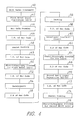
- Fig.4 is a block diagram illustrating the process flow involved in a master slice procedure.
- Figs. 5 to 11 give partial cross sectional views of a wafer at stages corresponding to specific steps in the process flow of Fig. 4.
- the left side of each Figure shows a chip area
- the right side shows a bar code pattern area near the orientation flat edge of a wafer.
- the chip area for the purposes of illustration, only one bipolar transistor is shown, as a typical active element.
- step 40 all bulk processes before a (first) metal deposition process are briefly represented as step 40.
- step 42 the step of depositing a metal layer 92 (usually an aluminum layer is employed) is finished, the wafer structure shown in Fig. 5 is obtained.
- p-type silicon substrate 80 is used, and n+ buried layer 81 is formed therein. Then n-type epitaxial layer 82 is grown thereon. Next, silicon dioxide 87 (field oxide film) is formed thereon, and then p+ isolation 83 is formed by implanting boron ions. Next, n+ collector contact 85, p-type base region 84 and n-type emitter region 86 are formed in succession by implanting phosphorus or boron impurity ions. Then, contact openings 88, 89, 90 are formed in silicon dioxide layer 87 in preparation for step 42 - the first metallization process (Al-I layer).
- Al-I layer the first metallization process
- n-type epitaxial layer 82 and silicon dioxide layer 87 are formed on p-type silicon substrate 80 in the region near the orientation flat edge (on the right in Fig. 5)
- the bar code pattern is first formed on the wafer, which is indicated as step 44 in Fig. 4.
- a bar code pattern on a wafer has been formed by a photolithography technique.
- the photolithography technique can provide a fine pattern consisting of a sequence of stripes having widths of 100 to 250 ⁇ m.
- the photolithography process involved requires an additional mask process and a considerable amount of lead time.
- a bar code pattern can be formed by a laser scribing method.
- a laser scriber which can form a bar code pattern having a width of 100 ⁇ m can be used.
- the aluminum can easily be melted and evaporated to form bar code pattern 5 in Fig. 6.
- the wafer is subjected to a process for patterning the first aluminum layer, called Al-I.
- This process consists of a series of process steps: resist coating 48, a photolithography process 50 including selection of a specific mask and exposure processes, development 54, and etching 56, and these steps are shown in Fig. 4.
- resist coating 48 resist coating 48
- a photolithography process 50 including selection of a specific mask and exposure processes
- development 54, and etching 56 and these steps are shown in Fig. 4.
- these steps should be preceded by identification steps 46, 49, 52 and 55, for identifying the wafer by detecting the bar code 5 because different wafers are expected to have different types of metal patterning, and are flowing mixed in the same production line.
- identification steps 46, 49, 52 and 55 for identifying the wafer by detecting the bar code 5 because different wafers are expected to have different types of metal patterning, and are flowing mixed in the same production line.
- detection of the bar code 5 is performed as explained in Figs. 1 and 2.
- interlayer insulator 94 is grown on an entire surface (step 60), as shown in Fig. 8.
- silicon dioxide phospho-silicate-glass (PSG), or silicon nitride can be used.
- step 64 an identification step 62, for identifying the wafer, and another photolithography process (step 64) are needed, and step 64 also comprises steps of resist coating, another identification of the wafer, mask selection, exposure, development, and etching. These steps are briefly put together and represented as single step 64.
- step 70 involving formation of a second metal (aluminum) layer 98 as indicated in Figs. 4 and 10.
- a window 100 should be formed in the metal layer 98, such that the metal layer 98 does not disturb the transmission of light through the wafer around the bar code pattern area.
- identification step 72 using the transmission of infrared rays through the wafer substrate at the bar code pattern 5, resist coating step 74 and photolithography step 76 and subsequent steps (the details are just the same as steps 52 through 56 explained in forming Al-I, and are omitted in Fig. 4) are followed.
- the second aluminum layer is patterned forming Al-II, which is shown in Fig. 11.
- the bar code pattern 5 is formed in the first metal (aluminum) layer 92, because the aluminum metal layer is the best material for interrupting the transmission of light.
- a bar code pattern formed on the silicon surface can sufficiently reduce the transmission of infrared rays.
- a bar code pattern which is scribed on the surface of silicon wafer 110 by a laser beam and is worked to have a rough surface 111 can be used for identification of wafers. Therefore, an embodiment of the present invention can be applied for identifying a bar code pattern which is directly formed on the silicon wafer 110 by laser scribing. In this case, a window is formed for all metal layers 92, 98 deposited on the bar code pattern area 5 such as the opening window 100 shown in Fig. 10.
- the arrangement of the light source 20 and detecting means 24 may be reversed, so that the light source 20 is located at the front side of semiconductor wafer 1 and the detector 24 is located at the back side thereof.
- the experiments indicate that better contrast can be obtained with an arrangement wherein the light source is located at the back side and the detector is located at the front side as shown in Fig. 1.
- a light source (20) which abundantly provides infrared light is positioned at the back side of the wafer (1) and a detector (24) at the front side thereof.
- the infrared light from the light source (20) easily penetrates the silicon wafer (1) and is received at the detector without any significant effect of reflection due to deposited layers on the front side of the wafer.
- the bar code pattern (5) is such as to selectively modify (e.g. selectively block) transmission of infrared light.
- a first metallization layer (Al-I) is a very suitable layer for use to form a bar code pattern, which can be easily formed in the layer by a laser beam scriber.
Landscapes
- Testing Or Measuring Of Semiconductors Or The Like (AREA)
- Dicing (AREA)
- Design And Manufacture Of Integrated Circuits (AREA)
Applications Claiming Priority (4)
| Application Number | Priority Date | Filing Date | Title |
|---|---|---|---|
| JP11642286 | 1986-05-20 | ||
| JP116422/86 | 1986-05-20 | ||
| JP14253386 | 1986-06-18 | ||
| JP142533/86 | 1986-06-18 |
Publications (2)
| Publication Number | Publication Date |
|---|---|
| EP0249762A1 true EP0249762A1 (de) | 1987-12-23 |
| EP0249762B1 EP0249762B1 (de) | 1991-05-08 |
Family
ID=26454749
Family Applications (1)
| Application Number | Title | Priority Date | Filing Date |
|---|---|---|---|
| EP87107307A Expired - Lifetime EP0249762B1 (de) | 1986-05-20 | 1987-05-20 | Identifizierung von Halbleiterscheiben mit Mustern des "Bar-code"-Typs |
Country Status (5)
| Country | Link |
|---|---|
| US (1) | US4825093A (de) |
| EP (1) | EP0249762B1 (de) |
| JP (1) | JPS63107014A (de) |
| KR (1) | KR900008384B1 (de) |
| DE (1) | DE3769858D1 (de) |
Cited By (4)
| Publication number | Priority date | Publication date | Assignee | Title |
|---|---|---|---|---|
| EP0488053A1 (de) * | 1990-11-29 | 1992-06-03 | Tokyo Seimitsu Co.,Ltd. | Methode zur Herstellung eines Halbleiterchips |
| EP0311087B1 (de) * | 1987-10-09 | 1993-02-10 | Fujitsu Limited | Identifizierung von Halbleiterplättchen |
| US5570293A (en) * | 1990-11-29 | 1996-10-29 | Tokyo Seimitsu Co., Ltd. | Method and device for manufacturing a semiconductor chip |
| US20230230863A1 (en) * | 2022-01-19 | 2023-07-20 | Ebara Corporation | Substrate conveyance method, substrate processing device, and recording medium |
Families Citing this family (30)
| Publication number | Priority date | Publication date | Assignee | Title |
|---|---|---|---|---|
| JP2523853B2 (ja) * | 1989-02-17 | 1996-08-14 | パイオニア株式会社 | 情報記録ディスク用スタンパ判別方法 |
| US5015832A (en) * | 1989-02-27 | 1991-05-14 | Kensington Laboratories, Inc. | Method of and apparatus for decoding bar code symbols |
| JP2734183B2 (ja) * | 1990-07-19 | 1998-03-30 | 日本電気株式会社 | 液晶表示素子 |
| DE4107069A1 (de) * | 1991-03-06 | 1992-09-10 | Leuze Electronic Gmbh & Co | Verfahren zum lesen von strichkodierungen auf halbleiteroberflaechen |
| DE69227175T2 (de) * | 1991-12-20 | 1999-04-29 | Eastman Kodak Co., Rochester, N.Y. | Aufzeichnungsträger für ein optisches Informationssystem mit eingebettetem Identifikationskode |
| DE4395834T1 (de) * | 1992-11-17 | 1994-12-01 | Kabusiki Kaisha Kakizaki Seisa | Aus Harz hergestellter Korb für dünne Folien |
| EP0682795A1 (de) * | 1993-02-02 | 1995-11-22 | Label Vision Systems, Inc. | Vorrichtung und verfahren zur dekodierung von strichkodierten daten aus einem videosignal und ihre anwendungen |
| JPH0744594U (ja) * | 1993-09-17 | 1995-11-21 | 東光株式会社 | 半導体ウエハ |
| US8505108B2 (en) * | 1993-11-18 | 2013-08-06 | Digimarc Corporation | Authentication using a digital watermark |
| US5740066A (en) * | 1995-07-03 | 1998-04-14 | Motorola, Inc. | Electrical circuit board and circuit board assembly |
| US5956596A (en) * | 1995-11-06 | 1999-09-21 | Samsung Electronics Co., Ltd. | Method of forming and cleaning a laser marking region at a round zone of a semiconductor wafer |
| JPH09320911A (ja) * | 1996-05-27 | 1997-12-12 | Mitsubishi Electric Corp | 被識別機能付き半導体基板 |
| CA2273815A1 (en) * | 1996-12-02 | 1998-06-11 | Cal Nichols | Tracking system for animal and carcasses |
| US6446017B1 (en) | 1997-08-21 | 2002-09-03 | Micron Technology, Inc. | Method and system for tracking manufacturing data for integrated circuit parts |
| US6268641B1 (en) * | 1998-03-30 | 2001-07-31 | Kabushiki Kaisha Toshiba | Semiconductor wafer having identification indication and method of manufacturing the same |
| US7313253B2 (en) * | 1998-09-11 | 2007-12-25 | Digimarc Corporation | Methods and tangible objects employing machine readable data in photo-reactive materials |
| JP2001194320A (ja) * | 2000-01-06 | 2001-07-19 | Advantest Corp | 表面状態測定装置及び方法 |
| US20040104361A1 (en) * | 2000-09-14 | 2004-06-03 | Guldi Richard L. | Semiconductor wafer edge marking |
| US7344900B2 (en) * | 2003-02-10 | 2008-03-18 | Texas Instruments Incorporated | Laser scribe on front side of semiconductor wafer |
| US8181884B2 (en) * | 2003-11-17 | 2012-05-22 | Digimarc Corporation | Machine-readable features for objects |
| US7415317B2 (en) * | 2004-02-25 | 2008-08-19 | Micron Technology, Inc. | Method and system for correlating and combining production and non-production data for analysis |
| US7395130B2 (en) * | 2004-02-27 | 2008-07-01 | Micron Technology, Inc. | Method and system for aggregating and combining manufacturing data for analysis |
| US20070125863A1 (en) * | 2005-12-05 | 2007-06-07 | Jakoboski Timothy A | System and method for employing infrared illumination for machine vision |
| US7544578B2 (en) | 2007-01-03 | 2009-06-09 | International Business Machines Corporation | Structure and method for stochastic integrated circuit personalization |
| DE102007058649A1 (de) * | 2007-12-04 | 2009-06-10 | Deutsche Solar Ag | Auslesen von Informationen auf Halbleiter-Substraten |
| CN102222601B (zh) * | 2010-04-14 | 2016-03-16 | 中芯国际集成电路制造(上海)有限公司 | 增强晶圆识别码清晰度的方法 |
| JP5674731B2 (ja) * | 2012-08-23 | 2015-02-25 | 東京エレクトロン株式会社 | 検査装置、接合システム、検査方法、プログラム及びコンピュータ記憶媒体 |
| US8822141B1 (en) | 2013-03-05 | 2014-09-02 | International Business Machines Corporation | Front side wafer ID processing |
| US9601436B2 (en) | 2014-06-06 | 2017-03-21 | Taiwan Semiconductor Manufacturing Co., Ltd | Method for semiconductor wafer alignment |
| US11122680B2 (en) | 2019-03-18 | 2021-09-14 | International Business Machines Corporation | Passive methods of loose die identification |
Citations (3)
| Publication number | Priority date | Publication date | Assignee | Title |
|---|---|---|---|---|
| US4292576A (en) * | 1980-02-29 | 1981-09-29 | The United States Of America As Represented By The Secretary Of The Air Force | Mask-slice alignment method |
| DE3138085A1 (de) * | 1981-09-24 | 1983-04-07 | Siemens AG, 1000 Berlin und 8000 München | Verfahren zur kennzeichnung von randsystemen auf halbleiterscheiben bei der herstellung von halbleiterbauelementen, insbesondere von integrierten halbleiter-schaltkreisen |
| US4585931A (en) * | 1983-11-21 | 1986-04-29 | At&T Technologies, Inc. | Method for automatically identifying semiconductor wafers |
Family Cites Families (9)
| Publication number | Priority date | Publication date | Assignee | Title |
|---|---|---|---|---|
| JPS4834352A (de) * | 1971-09-07 | 1973-05-18 | ||
| US4010355A (en) * | 1974-06-10 | 1977-03-01 | Motorola, Inc. | Semiconductor wafer having machine readable indicies |
| US4134066A (en) * | 1977-03-24 | 1979-01-09 | International Business Machines Corporation | Wafer indexing system using a grid pattern and coding and orientation marks in each grid cell |
| JPS5534442A (en) * | 1978-08-31 | 1980-03-11 | Fujitsu Ltd | Preparation of semiconductor device |
| JPS5827663B2 (ja) * | 1979-06-04 | 1983-06-10 | 富士通株式会社 | 半導体装置の製造方法 |
| JPS57206042A (en) * | 1981-05-28 | 1982-12-17 | Fujitsu Ltd | Method for checking wiring pattern of wafer |
| US4538059A (en) * | 1981-09-16 | 1985-08-27 | Itr International Time Limited | Identification card with concealed coding and a simple reader module to decode it |
| JPS5929433A (ja) * | 1982-08-11 | 1984-02-16 | Hitachi Ltd | 半導体基板のライフタイム測定方法 |
| JPS6142119A (ja) * | 1984-08-06 | 1986-02-28 | Nippon Kogaku Kk <Nikon> | 認識装置 |
-
1987
- 1987-05-15 KR KR1019870004822A patent/KR900008384B1/ko not_active Expired
- 1987-05-19 JP JP62121501A patent/JPS63107014A/ja active Granted
- 1987-05-19 US US07/051,398 patent/US4825093A/en not_active Expired - Lifetime
- 1987-05-20 EP EP87107307A patent/EP0249762B1/de not_active Expired - Lifetime
- 1987-05-20 DE DE8787107307T patent/DE3769858D1/de not_active Expired - Lifetime
Patent Citations (3)
| Publication number | Priority date | Publication date | Assignee | Title |
|---|---|---|---|---|
| US4292576A (en) * | 1980-02-29 | 1981-09-29 | The United States Of America As Represented By The Secretary Of The Air Force | Mask-slice alignment method |
| DE3138085A1 (de) * | 1981-09-24 | 1983-04-07 | Siemens AG, 1000 Berlin und 8000 München | Verfahren zur kennzeichnung von randsystemen auf halbleiterscheiben bei der herstellung von halbleiterbauelementen, insbesondere von integrierten halbleiter-schaltkreisen |
| US4585931A (en) * | 1983-11-21 | 1986-04-29 | At&T Technologies, Inc. | Method for automatically identifying semiconductor wafers |
Non-Patent Citations (5)
| Title |
|---|
| IBM TECHNICAL DISCLOSURE BULLETIN, vol. 25, no. 1, June 1982, pages 319-322, Armonk, New York, US; D.A. NIELSEN et al.: "Laser-written and -read symbol set of high radix" * |
| PATENT ABSTRACTS OF JAPAN, vol. 10, no. 197 (E-418)[2253], 10th July 1986; & JP-A-61 42 119 (NIPPON KOGAKU K.K.) 28-02-1986 * |
| PATENT ABSTRACTS OF JAPAN, vol. 7, no. 58 (E-163)[1203], 10th March 1983; & JP-A-57 206 042 (FUJITSU K.K.) 17-12-1982 * |
| PATENT ABSTRACTS OF JAPAN, vol. 8, no. 115 (E-247)[1552], 29th May 1984; & JP-A-59 29 433 (HITACHI SEISAKUSHO K.K.) 16-02-1984 * |
| SOLID STATE TECHNOLOGY, vol. 22, no. 6, June 1979, pages 77-79, Port Washington, New York, US; B.I.C.F. VAN PUL: "Coding and decoding of wafers" * |
Cited By (4)
| Publication number | Priority date | Publication date | Assignee | Title |
|---|---|---|---|---|
| EP0311087B1 (de) * | 1987-10-09 | 1993-02-10 | Fujitsu Limited | Identifizierung von Halbleiterplättchen |
| EP0488053A1 (de) * | 1990-11-29 | 1992-06-03 | Tokyo Seimitsu Co.,Ltd. | Methode zur Herstellung eines Halbleiterchips |
| US5570293A (en) * | 1990-11-29 | 1996-10-29 | Tokyo Seimitsu Co., Ltd. | Method and device for manufacturing a semiconductor chip |
| US20230230863A1 (en) * | 2022-01-19 | 2023-07-20 | Ebara Corporation | Substrate conveyance method, substrate processing device, and recording medium |
Also Published As
| Publication number | Publication date |
|---|---|
| EP0249762B1 (de) | 1991-05-08 |
| KR900008384B1 (ko) | 1990-11-17 |
| KR870011666A (ko) | 1987-12-26 |
| JPS63107014A (ja) | 1988-05-12 |
| US4825093A (en) | 1989-04-25 |
| JPH0577326B2 (de) | 1993-10-26 |
| DE3769858D1 (de) | 1991-06-13 |
Similar Documents
| Publication | Publication Date | Title |
|---|---|---|
| EP0249762B1 (de) | Identifizierung von Halbleiterscheiben mit Mustern des "Bar-code"-Typs | |
| US4896034A (en) | Method of identifying a semiconductor wafer utilizing a light source and a detector | |
| US4824254A (en) | Alignment marks on semiconductor wafers and method of manufacturing the marks | |
| JP3343026B2 (ja) | 半導体集積回路およびその製造方法 | |
| US5149671A (en) | Method for forming multilayer indium bump contact | |
| EP0212219B1 (de) | Verfahren zur Sichtbarkeitsverbesserung von Ausrichtmarkierungen erster Ordnung | |
| US6261918B1 (en) | Method for creating and preserving alignment marks for aligning mask layers in integrated circuit manufacture | |
| EP1164639B1 (de) | Ausrichtmarken zur Herstellung einer Halbleitervorrichtung | |
| US5786267A (en) | Method of making a semiconductor wafer with alignment marks | |
| US6586282B1 (en) | Method of manufacturing a semiconductor device | |
| US4468857A (en) | Method of manufacturing an integrated circuit device | |
| USRE30282E (en) | Double master mask process for integrated circuit manufacture | |
| JP2004289131A (ja) | 半導体装置及びその製造方法 | |
| US6468704B1 (en) | Method for improved photomask alignment after epitaxial process through 90° orientation change | |
| JPH06283663A (ja) | 半導体チップどうしを整合するための方法 | |
| JP2550671B2 (ja) | 半導体装置の製造方法とバーコードリーダ | |
| EP0377101B1 (de) | Referenzmarkierungsstruktur zur Justierung der Ausrichtung von unfertigen Topographien von integrierten Halbleiterschaltungen in Bezug auf aufeinanderfolgende Masken | |
| JPH05175496A (ja) | トランジスタの製法 | |
| US20250357212A1 (en) | Semiconductor wafer including frame identifier, method of processing a semiconductor wafer using frame identifier, and semiconductor chip | |
| JPH01304721A (ja) | 標識を有する半導体基板 | |
| JPH0817150B2 (ja) | 半導体製造装置の位置合わせ方法 | |
| JP2900380B2 (ja) | 半導体装置の製造方法 | |
| EP0631316A2 (de) | Halbleiterelement mit einer Ausrichtungsmarke, Verfahren zur Herstellung derselben und Ausrichtungsverfahren | |
| KR20020045743A (ko) | 반도체 소자의 웨이퍼 정렬용 마크 및 이를 이용한 웨이퍼정렬 방법 | |
| JP2924298B2 (ja) | ウェーハの品種コード識別システム |
Legal Events
| Date | Code | Title | Description |
|---|---|---|---|
| PUAI | Public reference made under article 153(3) epc to a published international application that has entered the european phase |
Free format text: ORIGINAL CODE: 0009012 |
|
| AK | Designated contracting states |
Kind code of ref document: A1 Designated state(s): DE FR GB |
|
| 17P | Request for examination filed |
Effective date: 19880209 |
|
| 17Q | First examination report despatched |
Effective date: 19891215 |
|
| GRAA | (expected) grant |
Free format text: ORIGINAL CODE: 0009210 |
|
| AK | Designated contracting states |
Kind code of ref document: B1 Designated state(s): DE FR GB |
|
| REF | Corresponds to: |
Ref document number: 3769858 Country of ref document: DE Date of ref document: 19910613 |
|
| ET | Fr: translation filed | ||
| PLBE | No opposition filed within time limit |
Free format text: ORIGINAL CODE: 0009261 |
|
| STAA | Information on the status of an ep patent application or granted ep patent |
Free format text: STATUS: NO OPPOSITION FILED WITHIN TIME LIMIT |
|
| 26N | No opposition filed | ||
| REG | Reference to a national code |
Ref country code: GB Ref legal event code: IF02 |
|
| PGFP | Annual fee paid to national office [announced via postgrant information from national office to epo] |
Ref country code: FR Payment date: 20020508 Year of fee payment: 16 |
|
| PGFP | Annual fee paid to national office [announced via postgrant information from national office to epo] |
Ref country code: GB Payment date: 20020515 Year of fee payment: 16 |
|
| PGFP | Annual fee paid to national office [announced via postgrant information from national office to epo] |
Ref country code: DE Payment date: 20020529 Year of fee payment: 16 |
|
| PG25 | Lapsed in a contracting state [announced via postgrant information from national office to epo] |
Ref country code: GB Free format text: LAPSE BECAUSE OF NON-PAYMENT OF DUE FEES Effective date: 20030520 |
|
| PG25 | Lapsed in a contracting state [announced via postgrant information from national office to epo] |
Ref country code: DE Free format text: LAPSE BECAUSE OF NON-PAYMENT OF DUE FEES Effective date: 20031202 |
|
| GBPC | Gb: european patent ceased through non-payment of renewal fee |
Effective date: 20030520 |
|
| PG25 | Lapsed in a contracting state [announced via postgrant information from national office to epo] |
Ref country code: FR Free format text: LAPSE BECAUSE OF NON-PAYMENT OF DUE FEES Effective date: 20040130 |
|
| REG | Reference to a national code |
Ref country code: FR Ref legal event code: ST |