EP0488212A2 - Schnittstellenschaltung zwischen mehreren Übertragungsleitungen und einer Datenendeeinrichtung mit hohem Datenfluss - Google Patents
Schnittstellenschaltung zwischen mehreren Übertragungsleitungen und einer Datenendeeinrichtung mit hohem Datenfluss Download PDFInfo
- Publication number
- EP0488212A2 EP0488212A2 EP91120272A EP91120272A EP0488212A2 EP 0488212 A2 EP0488212 A2 EP 0488212A2 EP 91120272 A EP91120272 A EP 91120272A EP 91120272 A EP91120272 A EP 91120272A EP 0488212 A2 EP0488212 A2 EP 0488212A2
- Authority
- EP
- European Patent Office
- Prior art keywords
- data
- receiving
- synchronized
- channels
- clock signals
- Prior art date
- Legal status (The legal status is an assumption and is not a legal conclusion. Google has not performed a legal analysis and makes no representation as to the accuracy of the status listed.)
- Withdrawn
Links
Images


Classifications
-
- H—ELECTRICITY
- H04—ELECTRIC COMMUNICATION TECHNIQUE
- H04J—MULTIPLEX COMMUNICATION
- H04J3/00—Time-division multiplex systems
- H04J3/02—Details
- H04J3/06—Synchronising arrangements
- H04J3/062—Synchronisation of signals having the same nominal but fluctuating bit rates, e.g. using buffers
- H04J3/0626—Synchronisation of signals having the same nominal but fluctuating bit rates, e.g. using buffers plesiochronous multiplexing systems, e.g. plesiochronous digital hierarchy [PDH], jitter attenuators
- H04J3/0629—Synchronisation of signals having the same nominal but fluctuating bit rates, e.g. using buffers plesiochronous multiplexing systems, e.g. plesiochronous digital hierarchy [PDH], jitter attenuators in a network, e.g. in combination with switching or multiplexing, slip buffers
Definitions
- the present invention relates to a transmission line interface circuit provided between a plurality of transmission lines and a piece of high bit rate data terminal equipment.
- a source of high bit rate data such as a HDTV (high definition television) apparatus
- HDTV high definition television
- Typical applications of the transmission line interface circuit are a piece of terminal equipment and a switching unit in a multi-point television conference system.
- such a transmission line interface circuit receives data from a plurality of transmission lines synchronizing with clock signal in the respective transmission lines, transfers received data to the high bit rate data terminal equipment synchronized with a clock signal of the terminal equipment, receives data from the terminal equipment synchronized with the clock signal of the terminal equipment, and transmits received data through the plurality of transmission lines synchronized with the timing of the respective transmission lines.
- frame phases of transmission frames in the plurality of channels are required to be aligned in the transmission line interface circuit.
- the size of construction for changing the timing with which each bit of data synchronized is required to be small.
- An object of the present invention is to provide a transmission line interface circuit, provided between a plurality of transmission lines and a piece of high bit rate data terminal equipment, of small size.
- Another object of the present invention is to provide a transmission line interface circuit, provided between a plurality of transmission lines and a piece of high bit rate data terminal equipment which can operate even when a trouble occurs in a part of the transmission lines.
- a transmission line interface circuit receiving a plurality of channels of data and a plurality of receiving clock signals respectively synchronized with the plurality of channels of data received from the respective transmission lines, allowing outputs of the plurality of channels of data synchronized with a master clock signal which is supplied from outside of the transmission line interface circuit, receiving a plurality of channels of data synchronized with the master clock signal, and outputting a plurality of transmitting clock signals and the plurality of channels of data respectively synchronized With the plurality of transmitting clock signals, comprising: a plurality of first synchronization timing changing circuits for receiving the plurality of channels of data synchronized with the respective receiving clock signals, and making each bit of the respective channels of data synchronized with a predetermined one of the plurality of receiving clock signals; a plurality of first FIFO circuits for inputting and holding each bit of the plurality of channels of data synchronized with the predetermined one of the plurality of receiving clock signals, and allowing outputs of the pluralit
- each of the plurality of first synchronizaton timing changing circuits may comprise, a first data latching circuit for latching a corresponding channel of data synchronized with a corresponding one of the plurality of receiving clock signals, an intermediate clock generating circuit for generating an intermediate clock signal, a second data latching circuit for receiving the corresponding channel of data latched in the first data latching circuit, and latching the corresponding channel of data synchronized with the intermediate clock signal, and a third data latching circuit for receiving the corresponding channel of data latched in the second data latching circuit, and latching the corresponding channel of data synchronized with the predetermined one of plurality of receiving clock signals.
- each intermediate clock generating circuit may comprise, a later clock timing detecting circuit for detecting a predetermined phase of one of the predetermined one of the plurality of receiving clock signals and the corresponding one of the plurality of receiving clock signals, where the phase of the clock signal is behind a phase of the other clock signal, and generating a pulse indicating the detected phase, and a delay circuit for delaying the phases of the pulse to generate the intermediate clock signal so that the phases of the corresponding receiving clock signal and the intermediate clock signal differ by an amount in a predetermined range, and the phases of the predetermined one of the plurality of receiving clock signals and the intermediate clock signal differ by an amount in a predetermined range.
- a transmission line interface circuit receiving a plurality of channels of data and a plurality of receiving clock signals respectively synchronized with the plurality of channels of data received from the respective transmission lines, allowing outputs of the plurality of channels of data synchronized with a master clock signal which is supplied from outside of the transmission line interface circuit, receiving a plurality of channels of data synchronized with the master clock signal, and outputting a plurality of transmitting clock signals and the plurality of channels of data respectively synchronized with the plurality of transmitting clock signals, comprising: a plurality of first synchronization timing changing circuits for receiving the plurality of channels of data synchronized with the respective receiving clock signals, and making each bit of the respective channels of data synchronized with a selected one of the plurality of receiving clock signals; a plurality of first FIFO circuits for inputting and holding each bit of the plurality of channels of data synchronized with the selected one of the plurality of receiving clock signals, and allowing outputs of the plurality of
- the transmission line interface circuit may further comprise a plurality of clock abnormality detecting circuits respectively for detecting abnormality occurring in the plurality of receiving clock signals, and the clock selecting circuit may select one receiving clock signal among the plurality of receiving clock signals on which abnormality is not detected by the plurality of clock abnormality detecting circuits.
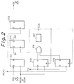
- Figures 1 is a diagram indicating a construction of the first embodiment of the present invention.
- reference numeral 101 denotes a unit containing a plurality of data receiving circuits (not shown) and a plurality of data transmitting circuits (not shown)
- 102 denotes a transmission line interface circuit according to the present invention
- 103 denotes a clock abnormality detecting circuit
- 104R2 ...
- 104Rn each denote a first data synchronization changing circuit, 104S1, ...
- 104Sn each denote a second data synchronization changing circuit
- 105R denotes a first data buffer memory circuit
- 105S denotes a second data buffer memory circuit
- 106 denotes a piece of data terminal equipment
- 108 denotes a resset signal generation circuit.
- the plurality of data receiving circuits and the plurality of data transmitting circuits are respectively connected to a plurality of transmission lines.
- the plurality of first data synchronization changing circuits 104R2, ... 104Rn are provided corresponding to the above plurality of data receiving circuits except a predetermined one of the plurality of data receiving circuits.
- Each of the plurality of first synchronization timing changing circuits 104R2, ⁇ 104Rn comprises a data input terminal, a data output terminal, and first and second clock input terminals.
- the receiving clock signal RCK1 from the above predetermined one of the data receiving circuits is applied to all the plurality of first data synchronization changing circuits 104R2, ... 104Rn.
- the first data buffer memory circuit 105R contains a plurality of FIFO memories each operating in parallel formation, where the plurality of FIFO memories are provided corresponding to the above plurality of data inputs RD1, RD2, ⁇ RDn.
- the data RD1 which is output from the above predetermined one of the plurality of data receiving circuits, is directly supplied to the data input terminal DI1.
- the above first data buffer memory circuit 105R is provided for detecting and aligning frames of data received in the plurality of data receiving circuits.
- the operation of detecting and aligning the frames is controlled by a controller provided in the transmission line interface circuit, but not shown.
- the piece of data terminal equipment 106 may be, for example, a piece of television conference terminal equipment which transmits and receives coded data of a television signal, or a switching unit in a multi-point television conference system.
- the operation of aligning the frames, is controlled by the above-mentioned controller.
- the second data buffer memory circuit 105S contains a plurality of FIFO memories each operating in parallel formation, where the plurality of FIFO memories are provided corresponding to the above plurality of channels of data SD1', SD2', ⁇ SDn'.
- the plurality of second data synchronization changing circuits 104S1, ⁇ 104Sn are provided corresponding to the above plurality of data transmitting circuits.
- Each of the plurality of second synchronization timing changing circuits 104S1, ⁇ 104Sn comprises a data input terminal, a data output terminal, and first and second clock input terminals.
- the reset signal generation circuit 108 generates reset signals which are to be applied to the first and second data buffer memory circuits 105R and 105S, respectively. These reset signals are used to align the frame phases of data in all the plurality of FIFO memories in the respective data buffer memory circuits 105R and 105S. Namely, one of the reset signals is applied to the FIFO memories in the first data buffer memory circuit 105R before a first bit in a frame in all the plurality of channels are to be written in the first data buffer memory circuit 105R, and the other of the reset signals is applied to the FIFO memories in the second data buffer memory circuit 105S before a first bit in a frame in all the plurality of channels are to be written in the second data buffer memory circuit 105S.
- the reset signal generation circuit 108 contains a frequency dividing circuit for generating the above reset signals from the above receiving clock signal RCK1.
- the ratio of the frequency division is generally very high, corresponding to a number of bits contained in each data frame.
- the frequency of the receiving clock signal RCK1 is, for example, 2MHz
- the frequency of the reset signal is, for example, 4KHz.
- a large number of stages of counters are required to construct such a high frequency division ratio, i.e., size of the frequency dividing circuit 108 is relatively large. This is the reason why the reset signal generation circuit 108 is provided common to all the FIFO memories in the respective data buffer memory circuits 105R and 105S.
- Figure 2 is a diagram indicating a construction of the first or second synchronization timing changing circuit in the construction of Fig. 1.
- reference numeral 311 to 415 each denote a D-type flip flop circuit
- 316 denotes an OR circuit
- 317 denotes a delay circuit.
- the above-mentioned receiving clock signal RCK1 from the predetermined one of the data receiving circuits is applied to the edge-triggered input terminals of the D-type flip flop circuits 313 and 315.
- the above-mentioned data RDi from the corresponding data receiving circuit is applied to the date input terminal of the D-type flip flop circuit 311, and the receiving clock signal RCKi from the same data receiving circuit is applied to the edge-triggered input terminals of the D-type flip flop circuits 311 and 314.
- the above-mentioned data DOi from the corresponding data output terminal of the second data buffer memory circuit is applied to the data input terminal of the D-type flip flop circuit 311, and the transmitting clock signal SCKi from the corresponding data transmitting circuit is applied to the edge-triggered input terminals of the D-type flip flop circuits 311 and 314.
- the data input terminals of the D-type flip flop circuits 314 and 315 are maintained to a high level +V.
- the data output D1 of the D-type flip flop circuit 311 is applied to the data input terminal of the D-type flip flop circuit 312, and the data output D2 of the D-type flip flop circuit 312 is applied to the data input terminal of the D-type flip flop circuit 313.
- the data outputs of the D-type flip flop circuits 314 and 315 are applied to the OR circuit 316, and the output of the OR circuit 316 is delayed by the delay circuit 317.
- the output TCK of the delay circuit 317 is applied to the edge-triggered input terminal of the D-type flip flop circuit 312, and the reset input terminals of the D-type flip flop circuits 314 and 315.
- the data output of the D-type flip flop circuit 313 is the output of the first or second synchronization timing changing circuit.
- the above data RDi from the corresponding data receiving circuit is latched in the D-type flip flop circuit 311 at timing of a leading edge of the receiving clock signal RCKi
- the data output of the D-type flip flop circuit 311 is latched in the D-type flip flop circuit 312 at timing of a leading edge of the output TCK of the delay circuit 317.
- the data outputs of the D-type flip flop circuits 314 and 315 rises when both the receiving clock signals RCK1 and RCKi transits to a high level state in each cycle of the receiving clock signals, and therefore, the output of the OR circuit 316 rises at the timing when one of the receiving clock signals RCK1 and RCKi the phase which is behind the phase of the other receiving clock signal, transits to a high level state.
- the output TCK of the delay circuit 317 rises a predetermined time later.
- the output TCK of the delay circuit 317 provides an intermediate clock signal.
- the intermediate clock signal TCR and the D-type flip flop circuit 312 are provided to prevent latching of a data output of a D-type flip flop circuit in a preceding stage, by a D-type flip flop circuit in the following stage at timing when the data output of a D-type flip flop circuit in a preceding stage is unstable.
- the delay time in the delay circuit 317 is preset so that the data output of the D-type flip flop circuit 311 is latched by the D-type flip flop circuit 312 at timing when the data output of the D-type flip flop circuit 311 is stable, and the data output of the D-type flip flop circuit 312 is latched by the D-type flip flop circuit 313 at timing when the data output of the D-type flip flop circuit 312 is stable.
- the delay time in the delay circuit 317 is preset so that the phases of the corresponding receiving clock signal and the intermediate clock signal differ by an amount in a predetermined range, and the phases of the predetermined one of the plurality of receiving clock signals and the intermediate clock signal differ by an amount in a predetermined range to realize the above effect.
- the delay time in the delay circuit 317 is preset so that the phases of the corresponding receiving clock signal and the intermediate clock signal differ by an amount in a predetermined range, and the phases of the predetermined one of the plurality of receiving clock signals and the intermediate clock signal differ by an amount in a predetermined range so that the data output of the D-type flip flop circuit 311 is latched by the D-type flip flop circuit 312 at timing when the data output of the D-type flip flop circuit 311 is stable, and the data output of the D-type flip flop circuit 312 is latched by the D-type flip flop circuit 313 at timing when the data output of the D-type flip flop circuit 312 is stable.
- Figure 3 is a diagram indicating example timing of the synchronization timing changing circuit.
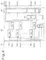
- Figure 4 is a diagram indicating a construction of the second embodiment of the present invention.
- reference numeral 10 denotes a unit containing a plurality of data receiving circuits (not shown) and a plurality of data transmitting circuits (not shown)
- 20 denotes a transmission line interface circuit according to the present invention
- ⁇ 30n each denote a first data synchronization changing circuit which functions the same as the first data synchronization changing circuit 104Ri in Fig. 1
- ⁇ 40n each denote a clock abnormality detecting circuit
- 50 denotes a first data buffer memory circuit which functions the same as the first data buffer memory circuit 105R in Fig.
- the plurality of data receiving circuits and the plurality of data transmitting circuits are respectively connected to a plurality of transmission lines.
- the clock abnormality detecting circuits 401, 402, ⁇ 40n are provided corresponding to the plurality of data receiving circuits in the unit 10, and each detect an occurrence of abnormality in the receiving clock signal which is output from the corresponding data receiving circuit in the unit 10.
- the results of the detection in the plurality of the clock abnormality detecting circuits 401, 402, ⁇ 40n, are applied to the selection control circuit 80, and the piece of data terminal equipment 60.
- an alarm is generated when the above results of the detection indicate an occurrence of abnormality in the receiving clock signals RCKi.
- the selected receiving clock signal which is denoted by RCK0 in Fig. 4, instead of the receiving clock signal RCK1 in the construction of Fig.
- the plurality of first data synchronization changing circuits 301, 302, ⁇ 30n are provided corresponding to all of the data receiving circuits in the unit 10.
- FIGS. 5A to 5G are diagrams indicating example timing of the second embodiment of the present invention.
- the selector 70 selects the receiving clock signal RCK1 as the common receiving clock signal RCK0, based on the detection results of the clock abnormality detecting circuits 401, 402, ⁇ 40n.
- the receiving clock signal RCK2 becomes normal at the time t2, and then the receiving clock signal RCKn becomes normal at the time tn.
- the receiving clock signal RCK1 becomes abnormal, and the abnormality is detected by the clock abnormality detecting circuit 401.
- the selection control circuit 80 determines the receiving clock signal RCK2, instead of the receiving clock signal RCK1, as the common receiving clock signal RCK0.
- the transmission and reception of data through the remaining transmission lines can be performed using one of the normal receiving clock signals as the common receiving clock signal RCK0.
- a reset signal generation circuit functioning the same as the reset signal generation circuit 108 in Fig. 1, is provided in the transmission line interface circuit in the second embodiment.
- the reset signal generation circuit in the second embodiment generates the reset signals synchronizing with the above common receiving clock signal RCK0, instead of the receiving clock signal RCK1 in the first embodiment.
Landscapes
- Engineering & Computer Science (AREA)
- Computer Hardware Design (AREA)
- Computer Networks & Wireless Communication (AREA)
- Signal Processing (AREA)
- Synchronisation In Digital Transmission Systems (AREA)
- Communication Control (AREA)
- Time-Division Multiplex Systems (AREA)
Applications Claiming Priority (2)
| Application Number | Priority Date | Filing Date | Title |
|---|---|---|---|
| JP327303/90 | 1990-11-27 | ||
| JP2327303A JPH04175028A (ja) | 1990-07-23 | 1990-11-27 | 多チャネル接続装置の伝送路インタフェース回路 |
Publications (2)
| Publication Number | Publication Date |
|---|---|
| EP0488212A2 true EP0488212A2 (de) | 1992-06-03 |
| EP0488212A3 EP0488212A3 (en) | 1993-03-17 |
Family
ID=18197625
Family Applications (1)
| Application Number | Title | Priority Date | Filing Date |
|---|---|---|---|
| EP19910120272 Withdrawn EP0488212A3 (en) | 1990-11-27 | 1991-11-27 | Interface circuit between a plurality of transmission lines and a high bit rate data terminal equipment |
Country Status (3)
| Country | Link |
|---|---|
| US (1) | US5268932A (de) |
| EP (1) | EP0488212A3 (de) |
| CA (1) | CA2056046C (de) |
Cited By (1)
| Publication number | Priority date | Publication date | Assignee | Title |
|---|---|---|---|---|
| US10873441B2 (en) * | 2019-03-29 | 2020-12-22 | Teledyne E2V Semiconductors Sas | Method for synchronizing digital data sent in series |
Families Citing this family (9)
| Publication number | Priority date | Publication date | Assignee | Title |
|---|---|---|---|---|
| US5832047A (en) * | 1994-06-17 | 1998-11-03 | International Business Machines Corporation | Self timed interface |
| JP3681225B2 (ja) * | 1996-07-31 | 2005-08-10 | 富士通株式会社 | シンクロナイゼイション・メッセージ送信装置 |
| US6765954B1 (en) * | 1999-08-16 | 2004-07-20 | Globespanvirata, Inc. | System and method for implementing a delta-sigma modulator integrity supervisor |
| US6577649B1 (en) * | 1999-11-12 | 2003-06-10 | International Business Machines Corporation | Multiplexer for asynchronous data |
| US6901526B1 (en) * | 2000-11-08 | 2005-05-31 | Intel Corporation | Digital bus synchronizer for generating read reset signal |
| US6807232B2 (en) * | 2000-12-21 | 2004-10-19 | National Instruments Corporation | System and method for multiplexing synchronous digital data streams |
| WO2003047134A2 (de) * | 2001-11-28 | 2003-06-05 | Bridgeco Ag | Verfahren zur synchronisation in netzwerken |
| US7593288B2 (en) * | 2007-12-19 | 2009-09-22 | International Business Machines Corporation | System for providing read clock sharing between memory devices |
| JP6467159B2 (ja) * | 2014-07-25 | 2019-02-06 | ローム株式会社 | パラレルインタフェースおよび集積回路 |
Family Cites Families (7)
| Publication number | Priority date | Publication date | Assignee | Title |
|---|---|---|---|---|
| JPS4811642B1 (de) * | 1966-11-19 | 1973-04-14 | ||
| US4133981A (en) * | 1977-12-19 | 1979-01-09 | Bell Telephone Laboratories, Incorporated | Time correction circuit for a digital multiplexer |
| JPS5841019B2 (ja) * | 1979-06-06 | 1983-09-09 | 富士通株式会社 | 回線多重化装置の2重化切替方式 |
| US4943942A (en) * | 1986-09-19 | 1990-07-24 | Advanced Micro Devices | Full-duplex modem using a single processor |
| US5040189A (en) * | 1987-01-12 | 1991-08-13 | Motorola, Inc. | Multiple frequency radio system employing pulse repeaters |
| JPH0817374B2 (ja) * | 1987-11-25 | 1996-02-21 | 日本電気株式会社 | クロツク伝送方法 |
| JPH0440030A (ja) * | 1990-06-05 | 1992-02-10 | Mitsubishi Electric Corp | 信号送受信装置 |
-
1991
- 1991-11-22 CA CA002056046A patent/CA2056046C/en not_active Expired - Fee Related
- 1991-11-26 US US07/797,935 patent/US5268932A/en not_active Expired - Lifetime
- 1991-11-27 EP EP19910120272 patent/EP0488212A3/en not_active Withdrawn
Cited By (1)
| Publication number | Priority date | Publication date | Assignee | Title |
|---|---|---|---|---|
| US10873441B2 (en) * | 2019-03-29 | 2020-12-22 | Teledyne E2V Semiconductors Sas | Method for synchronizing digital data sent in series |
Also Published As
| Publication number | Publication date |
|---|---|
| CA2056046C (en) | 1996-02-27 |
| EP0488212A3 (en) | 1993-03-17 |
| CA2056046A1 (en) | 1992-05-28 |
| US5268932A (en) | 1993-12-07 |
Similar Documents
| Publication | Publication Date | Title |
|---|---|---|
| US6816818B2 (en) | Method, clock generator module and receiver module for synchronizing a receiver module | |
| US5757871A (en) | Jitter suppression circuit for clock signals used for sending data from a synchronous transmission network to an asynchronous transmission network | |
| US5268932A (en) | Interface circuit between a plurality of transmission lines and high bit rate data terminal equipment | |
| EP0545392A2 (de) | Synchrone Schaltung | |
| US6163526A (en) | Transmission system for switching connection from a working channel line to a protection channel line while avoiding instantaneous cutoff upon failure | |
| US5946362A (en) | Apparatus for detecting clock failure for use in a synchronous transmission system | |
| US5677931A (en) | Transmission path switching apparatus | |
| EP0644664A2 (de) | System zur Anpassung der Eigenschaften einer Schutzeinheit | |
| US5123020A (en) | Phase synchronization pull-in system in bit error detecting apparatus | |
| NO157998B (no) | Synkron taktgenerator for digitalsignal-multipleksapparater. | |
| US4538110A (en) | High-stability clock signal regenerator with a stable fixed frequency backup clock generator | |
| EP0543327B1 (de) | Synchrones optisches Multiplexsystem | |
| US20020080825A1 (en) | Method and compensation module for the phase compensation of clock signals | |
| US5305322A (en) | Phase alignment circuit for stuffed-synchronized TDM transmission system with cross-connect function | |
| US5325354A (en) | Synchronous terminal station receiving system | |
| US6208648B1 (en) | Network element and input/output device for a synchronous transmission system | |
| KR0129608B1 (ko) | 분기 결합 제어장치 | |
| EP1168706B1 (de) | Verfahren und Schaltung zur Einphasung von Datenströmen in Zeitmultiplex-Rahmen | |
| JPH0338128A (ja) | 無瞬断切替方法 | |
| EP0409168A2 (de) | Schaltung zur elastischen Speicherung | |
| US7440765B2 (en) | Timing signal generation in telecommunications networks | |
| KR100397336B1 (ko) | 전송시스템의 멀티프레임펄스 안정화장치 | |
| KR0168921B1 (ko) | 동기식 전송시스템에서 시험액세스를 위한 24x3교차 스위치 회로 | |
| JPH01263566A (ja) | 伝送遅延差測定方式 | |
| KR100293941B1 (ko) | 데이타전송장치에서의프레임정렬데이타출력회로 |
Legal Events
| Date | Code | Title | Description |
|---|---|---|---|
| PUAI | Public reference made under article 153(3) epc to a published international application that has entered the european phase |
Free format text: ORIGINAL CODE: 0009012 |
|
| AK | Designated contracting states |
Kind code of ref document: A2 Designated state(s): DE FR GB |
|
| PUAL | Search report despatched |
Free format text: ORIGINAL CODE: 0009013 |
|
| AK | Designated contracting states |
Kind code of ref document: A3 Designated state(s): DE FR GB |
|
| 17P | Request for examination filed |
Effective date: 19930720 |
|
| 17Q | First examination report despatched |
Effective date: 19951222 |
|
| STAA | Information on the status of an ep patent application or granted ep patent |
Free format text: STATUS: THE APPLICATION IS DEEMED TO BE WITHDRAWN |
|
| 18D | Application deemed to be withdrawn |
Effective date: 19960702 |