EP0488546A1 - Contact pour circuits intégrés - Google Patents
Contact pour circuits intégrés Download PDFInfo
- Publication number
- EP0488546A1 EP0488546A1 EP19910310399 EP91310399A EP0488546A1 EP 0488546 A1 EP0488546 A1 EP 0488546A1 EP 19910310399 EP19910310399 EP 19910310399 EP 91310399 A EP91310399 A EP 91310399A EP 0488546 A1 EP0488546 A1 EP 0488546A1
- Authority
- EP
- European Patent Office
- Prior art keywords
- dielectric layer
- layer
- dielectric
- conductor
- integrated circuit
- Prior art date
- Legal status (The legal status is an assumption and is not a legal conclusion. Google has not performed a legal analysis and makes no representation as to the accuracy of the status listed.)
- Withdrawn
Links
Images
Classifications
-
- H—ELECTRICITY
- H10—SEMICONDUCTOR DEVICES; ELECTRIC SOLID-STATE DEVICES NOT OTHERWISE PROVIDED FOR
- H10W—GENERIC PACKAGES, INTERCONNECTIONS, CONNECTORS OR OTHER CONSTRUCTIONAL DETAILS OF DEVICES COVERED BY CLASS H10
- H10W20/00—Interconnections in chips, wafers or substrates
- H10W20/01—Manufacture or treatment
- H10W20/071—Manufacture or treatment of dielectric parts thereof
- H10W20/081—Manufacture or treatment of dielectric parts thereof by forming openings in the dielectric parts
-
- H—ELECTRICITY
- H10—SEMICONDUCTOR DEVICES; ELECTRIC SOLID-STATE DEVICES NOT OTHERWISE PROVIDED FOR
- H10W—GENERIC PACKAGES, INTERCONNECTIONS, CONNECTORS OR OTHER CONSTRUCTIONAL DETAILS OF DEVICES COVERED BY CLASS H10
- H10W20/00—Interconnections in chips, wafers or substrates
- H10W20/01—Manufacture or treatment
- H10W20/071—Manufacture or treatment of dielectric parts thereof
- H10W20/074—Manufacture or treatment of dielectric parts thereof of dielectric parts comprising thin functional dielectric layers, e.g. dielectric etch-stop, barrier, capping or liner layers
- H10W20/076—Manufacture or treatment of dielectric parts thereof of dielectric parts comprising thin functional dielectric layers, e.g. dielectric etch-stop, barrier, capping or liner layers in via holes or trenches
-
- H—ELECTRICITY
- H10—SEMICONDUCTOR DEVICES; ELECTRIC SOLID-STATE DEVICES NOT OTHERWISE PROVIDED FOR
- H10W—GENERIC PACKAGES, INTERCONNECTIONS, CONNECTORS OR OTHER CONSTRUCTIONAL DETAILS OF DEVICES COVERED BY CLASS H10
- H10W20/00—Interconnections in chips, wafers or substrates
- H10W20/40—Interconnections external to wafers or substrates, e.g. back-end-of-line [BEOL] metallisations or vias connecting to gate electrodes
- H10W20/45—Interconnections external to wafers or substrates, e.g. back-end-of-line [BEOL] metallisations or vias connecting to gate electrodes characterised by their insulating parts
- H10W20/48—Insulating materials thereof
Definitions
- the present invention relates generally to semiconductor integrated circuits, and more specifically to formation of a contact structure for such circuits.
- One type of structure commonly found on a semiconductor integrated circuit is a contact from an upper level metal interconnect layer to a lower conductive structure through a contact via.
- An interlevel dielectric through which the contact via is cut often has a reflow glass layer to improve planarity of the chip's surface.
- This glass layer typically has impurities which can migrate into the metal interconnect in the via and adversely affect its operation. For example, it is known that mobile ion donation from glass layers in contact with metal interconnect can shift data retention voltages in memory circuits. Also, outgassing of solvents in such a glass layer can cause voiding in, or oxidation of, sputtered metal interconnect.
- a method for forming a contact in a semiconductor integrated circuit includes the formation of a conformal oxide layer over the device followed by formation of a doped glass layer.
- the integrated circuit is heated to cause the glass layer to reflow, improving planarity of the circuit.
- a second conformal oxide layer is then formed, and contact vias are cut through the three part interlevel dielectric layer. Side walls are then formed in the via by depositing a third conformal layer, and anisotropically etching such layer. This isolates the doped reflowable glass layer from the via.
- Metal interconnect can then be deposited and defined, forming a contact in the via.
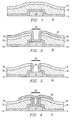
- Figures 1-4 illustrate a preferred method for forming a contact through an interlevel dielectric layer according to the present invention.
- a contact is to be formed on a semiconductor substrate 10 .
- Substrate 10 may be simply the substrate on which an integrated circuit is formed, or it may represent multiple lower layers which have already been fabricated. The details of any such multiple lower layers are not important to the present invention.
- Interconnect 12 is defined and patterned on the substrate 10 .
- Interconnect 12 may be a first metal level interconnect layer, or it may be polycrystalline silicon or a silicided polycrystalline silicon layer.
- a conformal dielectric layer 14 is deposited over the surface of the integrated circuit, followed by a reflowable glass layer 16 .
- Dielectric layer 14 is preferably an oxide layer, undoped or lightly doped as known in the art.
- Layer 14 is typically deposited using chemical vapor deposition (CVD) or low pressure chemical vapor deposition (LPCVD).
- reflowable glass layer 16 is typically amorphous silicon dioxide doped with impurities such as boron, to form boron doped silicate glass (BSG), or boron and phosphorus to form borophoso-silicate glass (BPSG).
- BSG boron doped silicate glass
- BPSG borophoso-silicate glass
- the integrated circuit is heated to cause the glass layer 16 to soften and partially flow into lower topographical regions on the integrated circuit. This heating is generally referred to as reflow. Heating may be performed by inserting the integrated circuit into a furnace, or through rapid thermal processing (RTP) as known in the art. Reflowing of glass layer 16 increases the planarity of its upper surface.
- RTP rapid thermal processing
- Another conformal dielectric layer 18 is then deposited over the glass layer 16 .
- Layer 18 is preferably a CVD or LPCVD oxide layer which is undoped or lightly doped.
- the three layers 14 , 16 , 18 together form an interlevel di
- a photomasking pattern (not shown) is used to define and etch contact via 20 .
- Via 20 provides an opening through the dielectric layers 14 , 16 , 18 to the interconnect layer 12 beneath.
- a conformal dielectric layer 22 is then deposited over the integrated circuit. This layer is also preferably an undoped oxide layer deposited using CVD or LPCVD techniques.
- the dielectric layer 22 is anisotropically etched to remove it from the horizontal surfaces of the integrated circuit. This leaves behind sidewall spacer structures 24 along the sidewalls of the contact via 20 .
- the anisotropic etch used to form spacers 24 will also typically remove a portion of dielectric layer 18 . Since over etching must be performed to ensure clearance of all oxide from the bottom of the contact via 20 , layer 18 is preferably thick enough to ensure that the reflowable glass layer 16 is not exposed by such over etch.
- the reflowable glass 16 is completely isolated from the contact via 20 by the sidewall spacers 24 . Since dielectric layer 18 was initially deposited with enough thickness to ensure that at least part of such layer remains after the anisotropic etch step, metal or other interconnect lying above the interlevel dielectric layer does not make contact with the glass layer 16 .
- interconnect layer 26 is deposited and patterned.
- Layer 26 can be a metal layer, such as aluminum, and can include a layer of refractory metal (not shown) beneath it as known in the art.
- Layer 26 could also be a polycrystalline silicon or silicided polycrystalline silicon layer as known in the art.
- interconnect layer 26 is separated from the reflow glass layer 16 by sidewall spacers 24 and dielectric layer 18 . This protects interconnect layer 26 from impurities contained within the reflow glass layer 16 .
- the method described above, and the structure formed thereby provides for isolation of an interconnect layer and contact from a reflow glass layer used for planarization of an integrated circuit.
- Formation of the upper layer 18 and sidewall spacers 24 adds a minimal amount of complexity to the process flow, and is compatible with standard process flows currently in use. This technique allows for improved contact formation while retaining the advantages of using a reflow glass for planarization.
Landscapes
- Internal Circuitry In Semiconductor Integrated Circuit Devices (AREA)
- Electrodes Of Semiconductors (AREA)
- Formation Of Insulating Films (AREA)
Applications Claiming Priority (2)
| Application Number | Priority Date | Filing Date | Title |
|---|---|---|---|
| US614296 | 1990-11-16 | ||
| US07/614,296 US5117273A (en) | 1990-11-16 | 1990-11-16 | Contact for integrated circuits |
Publications (1)
| Publication Number | Publication Date |
|---|---|
| EP0488546A1 true EP0488546A1 (fr) | 1992-06-03 |
Family
ID=24460639
Family Applications (1)
| Application Number | Title | Priority Date | Filing Date |
|---|---|---|---|
| EP19910310399 Withdrawn EP0488546A1 (fr) | 1990-11-16 | 1991-11-11 | Contact pour circuits intégrés |
Country Status (3)
| Country | Link |
|---|---|
| US (1) | US5117273A (fr) |
| EP (1) | EP0488546A1 (fr) |
| JP (1) | JPH04286330A (fr) |
Cited By (5)
| Publication number | Priority date | Publication date | Assignee | Title |
|---|---|---|---|---|
| EP0558260A1 (fr) * | 1992-02-28 | 1993-09-01 | STMicroelectronics, Inc. | Méthode de formation de vias de contact dans des circuits intégrés |
| EP0892428A3 (fr) * | 1997-07-17 | 1999-11-24 | Sharp Kabushiki Kaisha | Méthode de fabrication de contacts à faible résistance entre différents niveaux de couches métalliques dans un circuit intégré, et structures ainsi produites |
| EP0660393B1 (fr) * | 1993-12-23 | 2000-05-10 | STMicroelectronics, Inc. | Méthode et structure de diélectrique pour faciliter la surgravure de métal sans endommager le diélectrique intermédiaire |
| US6140222A (en) * | 1992-09-22 | 2000-10-31 | Lucent Technologies Inc. | Integrated circuit dielectric formation |
| EP0706211B1 (fr) * | 1994-10-05 | 2004-12-01 | Micronas GmbH | Structure de connections pour couches doubles |
Families Citing this family (26)
| Publication number | Priority date | Publication date | Assignee | Title |
|---|---|---|---|---|
| JP2669153B2 (ja) * | 1990-12-19 | 1997-10-27 | 日本電気株式会社 | 半導体装置の製造方法 |
| DE69225082T2 (de) * | 1991-02-12 | 1998-08-20 | Matsushita Electronics Corp | Halbleiter-Vorrichtung mit Verdrahtung der verbesserten Zuverlässigkeit und Verfahren zu ihner Herstellung |
| US5294295A (en) * | 1991-10-31 | 1994-03-15 | Vlsi Technology, Inc. | Method for moisture sealing integrated circuits using silicon nitride spacer protection of oxide passivation edges |
| US5424570A (en) * | 1992-01-31 | 1995-06-13 | Sgs-Thomson Microelectronics, Inc. | Contact structure for improving photoresist adhesion on a dielectric layer |
| US5321211A (en) * | 1992-04-30 | 1994-06-14 | Sgs-Thomson Microelectronics, Inc. | Integrated circuit via structure |
| US5317192A (en) * | 1992-05-06 | 1994-05-31 | Sgs-Thomson Microelectronics, Inc. | Semiconductor contact via structure having amorphous silicon side walls |
| KR960002073B1 (ko) * | 1992-06-10 | 1996-02-10 | 삼성전자주식회사 | 반도체 장치의 제조방법 |
| US5825078A (en) * | 1992-09-23 | 1998-10-20 | Dow Corning Corporation | Hermetic protection for integrated circuits |
| JP3271094B2 (ja) * | 1993-07-05 | 2002-04-02 | ソニー株式会社 | 積層配線基板及びその製造方法 |
| US5435888A (en) * | 1993-12-06 | 1995-07-25 | Sgs-Thomson Microelectronics, Inc. | Enhanced planarization technique for an integrated circuit |
| US6107194A (en) * | 1993-12-17 | 2000-08-22 | Stmicroelectronics, Inc. | Method of fabricating an integrated circuit |
| US6284584B1 (en) | 1993-12-17 | 2001-09-04 | Stmicroelectronics, Inc. | Method of masking for periphery salicidation of active regions |
| US5439846A (en) * | 1993-12-17 | 1995-08-08 | Sgs-Thomson Microelectronics, Inc. | Self-aligned method for forming contact with zero offset to gate |
| US5756397A (en) * | 1993-12-28 | 1998-05-26 | Lg Semicon Co., Ltd. | Method of fabricating a wiring in a semiconductor device |
| US6040020A (en) * | 1995-08-07 | 2000-03-21 | Micron Technology, Inc. | Method of forming a film having enhanced reflow characteristics at low thermal budget |
| JPH10509285A (ja) * | 1995-09-14 | 1998-09-08 | アドバンスト・マイクロ・ディバイシズ・インコーポレイテッド | 縮小したフィーチャーサイズのためのダマスクプロセス |
| US6130482A (en) * | 1995-09-26 | 2000-10-10 | Fujitsu Limited | Semiconductor device and method for fabricating the same |
| US5675185A (en) * | 1995-09-29 | 1997-10-07 | International Business Machines Corporation | Semiconductor structure incorporating thin film transistors with undoped cap oxide layers |
| JPH09116009A (ja) * | 1995-10-23 | 1997-05-02 | Sony Corp | 接続孔の形成方法 |
| US5683930A (en) | 1995-12-06 | 1997-11-04 | Micron Technology Inc. | SRAM cell employing substantially vertically elongated pull-up resistors and methods of making, and resistor constructions and methods of making |
| US6111319A (en) * | 1995-12-19 | 2000-08-29 | Stmicroelectronics, Inc. | Method of forming submicron contacts and vias in an integrated circuit |
| US5847460A (en) * | 1995-12-19 | 1998-12-08 | Stmicroelectronics, Inc. | Submicron contacts and vias in an integrated circuit |
| JP2809183B2 (ja) * | 1996-03-27 | 1998-10-08 | 日本電気株式会社 | 半導体記憶装置の製造方法 |
| US5913150A (en) * | 1997-04-11 | 1999-06-15 | Nec Corporation | Method for manufacturing semiconductor device using spin on glass layer |
| US5960315A (en) * | 1997-07-10 | 1999-09-28 | International Business Machines Corporation | Tapered via using sidewall spacer reflow |
| US6080672A (en) | 1997-08-20 | 2000-06-27 | Micron Technology, Inc. | Self-aligned contact formation for semiconductor devices |
Citations (2)
| Publication number | Priority date | Publication date | Assignee | Title |
|---|---|---|---|---|
| US4489481A (en) * | 1982-09-20 | 1984-12-25 | Texas Instruments Incorporated | Insulator and metallization method for VLSI devices with anisotropically-etched contact holes |
| EP0398834A2 (fr) * | 1989-05-15 | 1990-11-22 | International Business Machines Corporation | Procédé de formation des contacts dans un dispositif semi-conducteur |
Family Cites Families (3)
| Publication number | Priority date | Publication date | Assignee | Title |
|---|---|---|---|---|
| JPS54149469A (en) * | 1978-05-16 | 1979-11-22 | Toshiba Corp | Semiconductor device |
| US4972251A (en) * | 1985-08-14 | 1990-11-20 | Fairchild Camera And Instrument Corp. | Multilayer glass passivation structure and method for forming the same |
| US4962414A (en) * | 1988-02-11 | 1990-10-09 | Sgs-Thomson Microelectronics, Inc. | Method for forming a contact VIA |
-
1990
- 1990-11-16 US US07/614,296 patent/US5117273A/en not_active Expired - Lifetime
-
1991
- 1991-11-11 EP EP19910310399 patent/EP0488546A1/fr not_active Withdrawn
- 1991-11-14 JP JP3299230A patent/JPH04286330A/ja active Pending
Patent Citations (2)
| Publication number | Priority date | Publication date | Assignee | Title |
|---|---|---|---|---|
| US4489481A (en) * | 1982-09-20 | 1984-12-25 | Texas Instruments Incorporated | Insulator and metallization method for VLSI devices with anisotropically-etched contact holes |
| EP0398834A2 (fr) * | 1989-05-15 | 1990-11-22 | International Business Machines Corporation | Procédé de formation des contacts dans un dispositif semi-conducteur |
Non-Patent Citations (3)
| Title |
|---|
| IBM TECHNICAL DISCLOSURE BULLETIN. vol. 30, no. 8, January 1988, NEW YORK US pages 295 - 296; ANONYMOUS: 'Nitride sidewall apscers used as a contamination barrier' * |
| IBM TECHNICAL DISCLOSURE BULLETIN. vol. 32, no. 10B, March 1990, NEW YORK US pages 114 - 115; ANONYMOUS: 'Lithographic patterns with a barrier liner' * |
| PHILIPS JOURNAL OF RESEARCH. vol. 44, no. 2-3, 28 July 1989, EINDHOVEN NL pages 257 - 293; OSINSKI ET AL: 'A 0.1 um process for logic applications' * |
Cited By (7)
| Publication number | Priority date | Publication date | Assignee | Title |
|---|---|---|---|---|
| EP0558260A1 (fr) * | 1992-02-28 | 1993-09-01 | STMicroelectronics, Inc. | Méthode de formation de vias de contact dans des circuits intégrés |
| US5384483A (en) * | 1992-02-28 | 1995-01-24 | Sgs-Thomson Microelectronics, Inc. | Planarizing glass layer spaced from via holes |
| US5437763A (en) * | 1992-02-28 | 1995-08-01 | Sgs-Thomson Microelectronics, Inc. | Method for formation of contact vias in integrated circuits |
| US6140222A (en) * | 1992-09-22 | 2000-10-31 | Lucent Technologies Inc. | Integrated circuit dielectric formation |
| EP0660393B1 (fr) * | 1993-12-23 | 2000-05-10 | STMicroelectronics, Inc. | Méthode et structure de diélectrique pour faciliter la surgravure de métal sans endommager le diélectrique intermédiaire |
| EP0706211B1 (fr) * | 1994-10-05 | 2004-12-01 | Micronas GmbH | Structure de connections pour couches doubles |
| EP0892428A3 (fr) * | 1997-07-17 | 1999-11-24 | Sharp Kabushiki Kaisha | Méthode de fabrication de contacts à faible résistance entre différents niveaux de couches métalliques dans un circuit intégré, et structures ainsi produites |
Also Published As
| Publication number | Publication date |
|---|---|
| JPH04286330A (ja) | 1992-10-12 |
| US5117273A (en) | 1992-05-26 |
Similar Documents
| Publication | Publication Date | Title |
|---|---|---|
| US5117273A (en) | Contact for integrated circuits | |
| US5444019A (en) | Semiconductor contact via structure and method | |
| US6476488B1 (en) | Method for fabricating borderless and self-aligned polysilicon and metal contact landing plugs for multilevel interconnections | |
| EP0542477B1 (fr) | Procédé de fabrication d'un circuit intégré à contacts autoalignés entre des structures étroitement espacées | |
| US6285073B1 (en) | Contact structure and method of formation | |
| US5668052A (en) | Method of manufacturing semiconductor device | |
| KR910006370B1 (ko) | 반도체소자의 접속구멍형성방법 | |
| US20090004809A1 (en) | Method of Integration of a MIM Capacitor with a Lower Plate of Metal Gate Material Formed on an STI Region or a Silicide Region Formed in or on the Surface of a Doped Well with a High K Dielectric Material | |
| US6001726A (en) | Method for using a conductive tungsten nitride etch stop layer to form conductive interconnects and tungsten nitride contact structure | |
| US5234852A (en) | Sloped spacer for MOS field effect devices comprising reflowable glass layer | |
| JP2000082682A (ja) | 半導体―絶縁層の製造方法及びそれを有する素子の製造方法 | |
| JPH05226478A (ja) | 半導体構造用のスタッドを形成する方法および半導体デバイス | |
| JPS63313837A (ja) | 埋込み多重レベル間相互接続体装置 | |
| US4933297A (en) | Method for etching windows having different depths | |
| US20020130347A1 (en) | Formation of a frontside contact on silicon-on-insulator substrate | |
| JP2720796B2 (ja) | 半導体装置の製造方法 | |
| US6613672B1 (en) | Apparatus and process of fabricating a trench capacitor | |
| US5994228A (en) | Method of fabricating contact holes in high density integrated circuits using taper contact and self-aligned etching processes | |
| EP0520658B1 (fr) | Structure et procédé de fabrication de contacts dans des dispositifs CMOS | |
| US6316816B1 (en) | Film resistor and method of producing same | |
| EP0566253A1 (fr) | Procédé pour la fabrication de structures de contact dans des circuits intégrés | |
| EP0164186A1 (fr) | Procédé de fabrication de dispositifs CMOS | |
| US6074923A (en) | Method of fabricating metal-oxide-semiconductor transistor | |
| US5923584A (en) | Dual poly integrated circuit interconnect | |
| US6146997A (en) | Method for forming self-aligned contact hole |
Legal Events
| Date | Code | Title | Description |
|---|---|---|---|
| PUAI | Public reference made under article 153(3) epc to a published international application that has entered the european phase |
Free format text: ORIGINAL CODE: 0009012 |
|
| AK | Designated contracting states |
Kind code of ref document: A1 Designated state(s): DE FR GB IT |
|
| RIN1 | Information on inventor provided before grant (corrected) |
Inventor name: CLARK, WAYNE DAVID Inventor name: STARK, DAVID MICHAEL |
|
| 17P | Request for examination filed |
Effective date: 19921126 |
|
| 17Q | First examination report despatched |
Effective date: 19971029 |
|
| RAP3 | Party data changed (applicant data changed or rights of an application transferred) |
Owner name: STMICROELECTRONICS, INC. |
|
| STAA | Information on the status of an ep patent application or granted ep patent |
Free format text: STATUS: THE APPLICATION IS DEEMED TO BE WITHDRAWN |
|
| 18D | Application deemed to be withdrawn |
Effective date: 19990601 |