EP0488566A2 - Verfahren und Vorrichtung zur Auswahl von schnellem Seitenmodus - Google Patents
Verfahren und Vorrichtung zur Auswahl von schnellem Seitenmodus Download PDFInfo
- Publication number
- EP0488566A2 EP0488566A2 EP91310652A EP91310652A EP0488566A2 EP 0488566 A2 EP0488566 A2 EP 0488566A2 EP 91310652 A EP91310652 A EP 91310652A EP 91310652 A EP91310652 A EP 91310652A EP 0488566 A2 EP0488566 A2 EP 0488566A2
- Authority
- EP
- European Patent Office
- Prior art keywords
- memory
- address
- data
- access
- cache
- Prior art date
- Legal status (The legal status is an assumption and is not a legal conclusion. Google has not performed a legal analysis and makes no representation as to the accuracy of the status listed.)
- Withdrawn
Links
Images


Classifications
-
- G—PHYSICS
- G06—COMPUTING OR CALCULATING; COUNTING
- G06F—ELECTRIC DIGITAL DATA PROCESSING
- G06F12/00—Accessing, addressing or allocating within memory systems or architectures
- G06F12/02—Addressing or allocation; Relocation
- G06F12/08—Addressing or allocation; Relocation in hierarchically structured memory systems, e.g. virtual memory systems
- G06F12/10—Address translation
- G06F12/1027—Address translation using associative or pseudo-associative address translation means, e.g. translation look-aside buffer [TLB]
- G06F12/1045—Address translation using associative or pseudo-associative address translation means, e.g. translation look-aside buffer [TLB] associated with a data cache
- G06F12/1054—Address translation using associative or pseudo-associative address translation means, e.g. translation look-aside buffer [TLB] associated with a data cache the data cache being concurrently physically addressed
-
- G—PHYSICS
- G06—COMPUTING OR CALCULATING; COUNTING
- G06F—ELECTRIC DIGITAL DATA PROCESSING
- G06F12/00—Accessing, addressing or allocating within memory systems or architectures
- G06F12/02—Addressing or allocation; Relocation
- G06F12/08—Addressing or allocation; Relocation in hierarchically structured memory systems, e.g. virtual memory systems
- G06F12/0802—Addressing of a memory level in which the access to the desired data or data block requires associative addressing means, e.g. caches
- G06F12/0877—Cache access modes
- G06F12/0882—Page mode
-
- G—PHYSICS
- G06—COMPUTING OR CALCULATING; COUNTING
- G06F—ELECTRIC DIGITAL DATA PROCESSING
- G06F12/00—Accessing, addressing or allocating within memory systems or architectures
- G06F12/02—Addressing or allocation; Relocation
- G06F12/08—Addressing or allocation; Relocation in hierarchically structured memory systems, e.g. virtual memory systems
- G06F12/0802—Addressing of a memory level in which the access to the desired data or data block requires associative addressing means, e.g. caches
- G06F12/0877—Cache access modes
- G06F12/0884—Parallel mode, e.g. in parallel with main memory or CPU
Definitions
- the present invention relates to the field of memory apparatus in digital systems. Specifically the present invention relates to the time saving technique of detecting both cache mode and fast page mode in the same clock cycle.
- Cache memories are used to somewhat minimize the time penalties due to accesses to main memory.
- Cache memories are relatively small, high speed buffer memories used in computer systems to temporarily hold those portions of the contents of memory which are currently in use. Information located in the cache memory may be accessed in less time than information located in main memory.
- the advantages of cache memories are derived from the property of locality with respect to memory accesses in a computer system. Two types of locality exist, temporal and spatial. Temporal locality reflects the observation that information which will be in use in the near future is likely to be in use already.
- DRAM Dynamic Random Access Memory
- fast page mode DRAMs are used as the main memory and allow for faster access to a memory location provided it is accessing the same row address as the previous memory access. DRAM access times are divided into random access times and column (or fast page mode) access times.
- Fast page mode DRAMs allow repeated access to the same row, with the benefit of not incurring the RAS precharge and RAS setup delays.
- Fast page mode DRAMs take advantage of the program behavior known as spatial locality, which describes the tendency of program data to access a narrow region of memory over a given amount of time.
- the comparator is located in the memory control unit (MCU).
- the MCU drives the DRAM control signal lines and determines if the current memory access may take advantage of a fast page mode access, or incur the additional delay of a random access.
- the fast page mode access capability improves performance by taking advantage of spatial locality; however, a price is paid in terms of the delay incurred by the row address comparator. In a synchronous system, this may add an additional cycle to all memory accesses.
- Early memory designs tended to accelerate only overlapping memory accesses, and defaulted to a random access mode (in which all DRAM control signals return to inactive) as the default, or idle, state.
- Recent high performance memory control designs have improved upon previous designs by implementing the last page mode access as the default access type. This requires that the row address for each memory access be checked before the access begins, to determine if the correct row is being accessed. The memory controller determines which type of memory access is appropriate before initiating the memory access. In a synchronous design, the comparison requires an additional clock cycle for all memory accesses. However, because last page mode access is normally two or three times faster than random access mode, a single state or cycle penalty on all memory accesses still increases overall performance over a system that does not implement fast page mode access.
- the memory management unit In a memory system containing a cache memory for a memory access, the memory management unit (MMU) first determines if the data being accessed is resident in the cache. If the data is found in the cache, the memory access is satisfied without accessing main memory. If the data is not resident in the cache, the MMU notifies the MCU that access to main memory is required. In a synchronous system, the cache lookup requires one or more states or clock cycles to determine if a main memory access is required. Additionally, if more than one processor is present, or if an I/O subsystem that supports direct memory access (DMA) is present, arbitration for memory access must also take place.
- DMA direct memory access
- FIG. 1 An illustrative computer system is shown in Fig. 1 .
- a computer 101 which comprises three major components. The first of these is the input/output (I/O) circuit 102 which is used to communicate information in appropriately structured form to and from the other parts of the computer 101.
- the central processing unit (CPU) 103 and memory subsystem 104 are also shown in Fig. 1 .
- an input device 105 shown in typical embodiment as a keyboard. It should be understood, however, that the input device may actually be a card reader, magnetic or paper tape reader, or other well-known input device (including, of course, another computer).
- a display monitor 107 is illustrated which is used to display messages or other communications to the user.
- a cursor control 109 is used to select command modes and edit the input data, and in general provides a more convenient means to input information into the system.
- the memory subsystem 104 comprises a memory management unit (MMU) 112, a memory control unit (MCU) 114, a cache 116, main memory 118, and an input/output interface 110 which connects to the mass memory 106.
- Mass memory 106 is connected to the computer 101 as a peripheral device and may be a disk drive, tape drive or the like.
- the main memory 118 is a DRAM which provides for fast page mode access.
- MMU 112 receives a data request from the CPU, performs any address translation from virtual to physical that is needed, and determines whether the data is located in mass memory 106, in main memory 118 or in the cache 116. If the data is located in the cache 116, a signal is sent to retrieve the data from the cache 116 and return the data to the MMU for transmission to the CPU 103. If the data is not located in the cache 116, a signal is sent to the MCU 114 to retrieve the requested data from main memory 118. The MCU 114 drives the signal lines (i.e., row, column lines) to access the memory location containing the requested data.
- signal lines i.e., row, column lines
- the MCU 114 prior to driving the signal lines, will compare the row address of the data to be accessed with the row address previously accessed. If the row addresses are the same, a quick access of the data can be achieved by executing a fast page mode cycle in which only the column address and CAS are required to access the correct location. If the row addresses are not the same, the MCU 114 must execute a random access cycle and incur the additional delay.
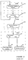
- a processor memory request 210 is initiated by the processor (i.e., CPU). This request is directed to the Memory Management Unit (MMU) which performs a cache lookup 220 to determine if the data requested is currently located in the cache. If the data is located in the cache, a "hit" occurs and the data is quickly transferred to the processor.
- MMU Memory Management Unit
- a "miss" occurs and the process continues by initiating a main memory access request 230 and performing any necessary arbitration (which is needed if the input/output subsystem has the ability to do direct memory access, if the system is a multiple processor system or if the CPU design incorporates separate instruction and data caches, where each cache can independently request a memory access).
- the main memory access request is directed to the memory control unit (MCU) which performs a row address comparison 240 to determine whether data is located at the same row address as the previous data accessed. If the data is located at the same row address, a hit occurs and the fast page mode access 250 is employed. If a miss occurs a slower random access of memory 260 is performed to access the data requested.
- MCU memory control unit
- the memory request logic is centralized in the memory management unit (MMU).
- the MMU instructs the MCU, which interfaces directly with the DRAMs, on the type of memory access to perform.
- the MMU is able to maintain an account of each memory access, thereby providing the MMU the means to determine if a memory access fulfills the requirements of a fast page mode access before a request is made to the MCU.
- the MMU comprises the row address comparator which can execute the row address comparison in parallel with the cache lookup. Therefore, if the cache lookup determines a memory access is required, a specific fast page mode memory access request can be made, without the memory controller incurring the additional delay of checking the row address.
- the system can default to fast page mode access without the additional penalty normally incurred by comparing the row address in a serial manner.
- the manipulations performed are often referred to in terms, such as adding or comparing, which are commonly associated with mental operations performed by a human operator. No such capability of a human operator is necessary, or desirable in most cases, in any of the operations described herein which form part of the present invention; the operations are machine operations.
- Useful machines for performing the operations of the present invention include general purpose digital computers or other similar devices. In all cases there should be borne in mind the distinction between the method operations in operating a computer and the method of computation itself.
- the present invention relates to method steps for operating a computer in processing electrical or other (e.g., mechanical, chemical) physical signals to generate other desired physical signals.
- the present invention also relates to apparatus for performing these operations.
- This apparatus may be specially constructed for the required purposes or it may comprise a general purpose computer as selectively activated or reconfigured by a computer program stored in the computer.
- the algorithms presented herein are not inherently related to a particular computer or other apparatus.
- various general purpose machines may be used with programs written in accordance with the teachings herein, or it may prove more convenient to construct more specialized apparatus to perform the required method steps. The required structure for a variety of these machines will appear from the description given below.
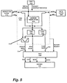
- Fig. 4 illustrates the memory sub-system of the present invention. Although the preferred embodiment illustrates a multiple cache system, it should be understood that the present invention is not limited as such and is applicable to a variety of system configurations including a system having a single cache.
- the memory management unit 300 receives the data request from the CPU 302, performs any address translation from virtual to physical that is needed in the Address Translation Block 304, determines whether the data is located in main memory 306 or in the data or instruction cache 308, 310.
- the MMU While determining whether the data is located in one of the caches 308, 310, and using a row address comparator 312 located in the MMU 300, the MMU also determines whether the fast page mode may be used to access data in main memory by comparing the row address of the data to be accessed with the row address of the data previously accessed.
- the tests to be performed to determine whether the data is located in the cache and whether a fast page mode access can be performed in a main memory access can be executed concurrently thereby saving the time needed to perform the tests in a serial manner.
- a separate column address bus 314 and multiplexor 316 are provided in order that the MCU 318 has quick access to the column address.
- an address is translated it is stored in the Physical Address Register (PAR) 320.
- PAR Physical Address Register
- a bypass data path is provided by the multiplexor 316 and column address bus 314.
- the column address is also directed to the multiplexor 316 which forwards the column address onto the column address bus 314 to the MCU 318.
- the multiplexor 316 causes the column address output from the PAR 320 to be placed on the column address bus 314 for input to the MCU 318.
- the bypass data path provides the column address to MCU one clock cycle sooner.
- a state machine (not shown) is utilized to control accesses to cache and memory. If a cache miss occurs, the state machine indicates that a memory access is to be performed. The state machine also allows, via multiple cache system, subsequent address translations as well as I/O translations to be performed while waiting for the data to be returned from a main memory read request. The state machine further controls the next main memory access to be performed. In order to accommodate fast page mode accessing of the present invention the state machine recognizes which addresses access data in a cache and which access main memory such that the row address comparator 312 always compares the row address of the last data retrieved from main memory. The state machine maintains the address of the last main memory access for input to the row address comparator 312.
- the state machine will maintain the row address of the last access to main memory and cause that row address to be input to the row address comparator to determine whether a fast page mode access can be performed.
- the MMU using row address comparator 312, already has determined whether a fast page mode access can be executed and based upon that determination, a signal is sent to the memory control unit 114 to either retrieve the requested data from main memory 118 using either a fast page mode access or the slower random access.
- the MCU through the column address bus 314, has the addressing information to perform the fast page mode access which permits it to immediately perform the last page mode access upon receipt of the signal from the MMU (via page mode line 322).
- the MCU 318 no longer incurs the delay to perform the row address comparison in order to determine whether the fast page mode access can be employed; the MMU has already performed the task.
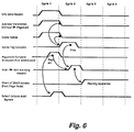
- Fig. 5 The process flow is illustrated by Fig. 5 .
- the MMU performs any needed virtual to physical address translation and memory arbitration as well as concurrently performing a cache lookup 310, to determine whether the data is located in the cache, and a row address comparison 320, to determine if the row address of the data to be accessed is the same row address as the data previously accessed from main memory by permitting a fast page mode access of main memory.
- the MMU determines that the data is located in the cache, the data is retrieved from the cache and returned to the CPU in response to the memory request. If the data is not in the cache, the MMU will already have determined whether a fast page mode access can be performed (from the row address comparison) and will immediately send a signal to the MCU to access the data using either the fast page mode access 340 or random access 350. Therefore, the extra time typically needed for the MCU to perform the row address comparison is saved thereby decreasing the amount of latency incurred when retrieving data from main memory in a cache based memory subsystem.
- a fast page mode access can be initiated at the beginning of the third clock cycle.
- the address translation, cache lookup and page mode comparison occur. If the cache tag comparison determines a cache miss and the MMU ⁇ MCU memory request line goes active, the fast page mode access is initiated at the beginning of the next clock cycle.
- a comparison of the timing diagram of Fig. 6 with the timing diagram of Fig. 3 shows that the present invention decreases the latency by one clock cycle over prior art methods when performing a fast page mode access.
Landscapes
- Engineering & Computer Science (AREA)
- Theoretical Computer Science (AREA)
- Physics & Mathematics (AREA)
- General Engineering & Computer Science (AREA)
- General Physics & Mathematics (AREA)
- Memory System Of A Hierarchy Structure (AREA)
- Memory System (AREA)
Applications Claiming Priority (2)
| Application Number | Priority Date | Filing Date | Title |
|---|---|---|---|
| US61987390A | 1990-11-29 | 1990-11-29 | |
| US619873 | 1990-11-29 |
Publications (2)
| Publication Number | Publication Date |
|---|---|
| EP0488566A2 true EP0488566A2 (de) | 1992-06-03 |
| EP0488566A3 EP0488566A3 (en) | 1992-10-21 |
Family
ID=24483671
Family Applications (1)
| Application Number | Title | Priority Date | Filing Date |
|---|---|---|---|
| EP19910310652 Withdrawn EP0488566A3 (en) | 1990-11-29 | 1991-11-19 | Method and apparatus for fast page mode selection |
Country Status (4)
| Country | Link |
|---|---|
| EP (1) | EP0488566A3 (de) |
| JP (1) | JPH0628239A (de) |
| KR (1) | KR960007833B1 (de) |
| CA (1) | CA2056512A1 (de) |
Cited By (3)
| Publication number | Priority date | Publication date | Assignee | Title |
|---|---|---|---|---|
| WO1993024885A1 (en) * | 1992-06-04 | 1993-12-09 | Cabletron Systems, Inc. | Adaptive memory controller |
| US5344636A (en) * | 1991-11-27 | 1994-09-06 | Kabushiki Kaisha Kaisui Kagaku Kenkyujo | Anti-microorganism agent and anti-microorganism resin or rubber composition |
| US6279082B1 (en) | 1998-10-14 | 2001-08-21 | Telefonaktiebolaget Lm Ericsson (Publ) | System and method for efficient use of cache to improve access to memory of page type |
Families Citing this family (4)
| Publication number | Priority date | Publication date | Assignee | Title |
|---|---|---|---|---|
| JP3739797B2 (ja) * | 1995-10-06 | 2006-01-25 | パトリオット サイエンティフィック コーポレイション | 縮小命令セット・コンピューター・マイクロプロセッサーの構造 |
| WO1998003918A1 (fr) * | 1996-07-19 | 1998-01-29 | Hitachi, Ltd. | Dispositif d'antememoire et systeme de traitement d'informations |
| KR20010011281A (ko) * | 1999-07-27 | 2001-02-15 | 서평원 | 음성 제공 장치에서의 안내방송 저장 방법 |
| KR100430305B1 (ko) * | 2001-07-21 | 2004-05-04 | 엘지전자 주식회사 | 음성 데이터 서비스 보드의 음성 메시지 변경 장치 및 방법 |
Family Cites Families (4)
| Publication number | Priority date | Publication date | Assignee | Title |
|---|---|---|---|---|
| US4785398A (en) * | 1985-12-19 | 1988-11-15 | Honeywell Bull Inc. | Virtual cache system using page level number generating CAM to access other memories for processing requests relating to a page |
| JPS635444A (ja) * | 1986-06-25 | 1988-01-11 | Hitachi Ltd | マイクロプロセツサ |
| US4847758A (en) * | 1987-10-30 | 1989-07-11 | Zenith Electronics Corporation | Main memory access in a microprocessor system with a cache memory |
| JPH04233642A (ja) * | 1990-07-27 | 1992-08-21 | Dell Usa Corp | キャッシュアクセスと並列的にメモリアクセスを行なうプロセッサ及びそれに用いられる方法 |
-
1991
- 1991-11-19 EP EP19910310652 patent/EP0488566A3/en not_active Withdrawn
- 1991-11-28 KR KR1019910021605A patent/KR960007833B1/ko not_active Expired - Fee Related
- 1991-11-28 CA CA002056512A patent/CA2056512A1/en not_active Abandoned
- 1991-11-29 JP JP3339413A patent/JPH0628239A/ja active Pending
Cited By (4)
| Publication number | Priority date | Publication date | Assignee | Title |
|---|---|---|---|---|
| US5344636A (en) * | 1991-11-27 | 1994-09-06 | Kabushiki Kaisha Kaisui Kagaku Kenkyujo | Anti-microorganism agent and anti-microorganism resin or rubber composition |
| WO1993024885A1 (en) * | 1992-06-04 | 1993-12-09 | Cabletron Systems, Inc. | Adaptive memory controller |
| AU660559B2 (en) * | 1992-06-04 | 1995-06-29 | Cabletron Systems, Inc. | Adaptive memory controller |
| US6279082B1 (en) | 1998-10-14 | 2001-08-21 | Telefonaktiebolaget Lm Ericsson (Publ) | System and method for efficient use of cache to improve access to memory of page type |
Also Published As
| Publication number | Publication date |
|---|---|
| JPH0628239A (ja) | 1994-02-04 |
| KR960007833B1 (ko) | 1996-06-12 |
| CA2056512A1 (en) | 1992-05-30 |
| KR920010446A (ko) | 1992-06-26 |
| EP0488566A3 (en) | 1992-10-21 |
Similar Documents
| Publication | Publication Date | Title |
|---|---|---|
| US5265236A (en) | Method and apparatus for increasing the speed of memory access in a virtual memory system having fast page mode | |
| US6317810B1 (en) | Microprocessor having a prefetch cache | |
| US5499355A (en) | Prefetching into a cache to minimize main memory access time and cache size in a computer system | |
| US6298424B1 (en) | Computer system including priorities for memory operations and allowing a higher priority memory operation to interrupt a lower priority memory operation | |
| US6449671B1 (en) | Method and apparatus for busing data elements | |
| US7412566B2 (en) | Memory hub and access method having internal prefetch buffers | |
| US5996061A (en) | Method for invalidating data identified by software compiler | |
| US5388247A (en) | History buffer control to reduce unnecessary allocations in a memory stream buffer | |
| US5694568A (en) | Prefetch system applicable to complex memory access schemes | |
| US6226722B1 (en) | Integrated level two cache and controller with multiple ports, L1 bypass and concurrent accessing | |
| CA1322058C (en) | Multi-processor computer systems having shared memory and private cache memories | |
| US6138208A (en) | Multiple level cache memory with overlapped L1 and L2 memory access | |
| US6138212A (en) | Apparatus and method for generating a stride used to derive a prefetch address | |
| JP3289661B2 (ja) | キャッシュメモリシステム | |
| EP1029280B1 (de) | Cache-speicherbetrieb | |
| KR20050005553A (ko) | 내부 캐쉬 및/또는 메모리 액세스 예측을 지닌 메모리 허브 | |
| JPH06243039A (ja) | キャッシュメモリシステムおよびマイクロプロセッサ内の命令を操作するための方法 | |
| KR100386638B1 (ko) | 외부메모리로의액세스요청을파이프라이닝하는마이크로프로세서 | |
| JP2001060169A (ja) | キャッシュコントローラ及びコンピュータシステム | |
| US5161219A (en) | Computer system with input/output cache | |
| US5367657A (en) | Method and apparatus for efficient read prefetching of instruction code data in computer memory subsystems | |
| US5835947A (en) | Central processing unit and method for improving instruction cache miss latencies using an instruction buffer which conditionally stores additional addresses | |
| EP0488566A2 (de) | Verfahren und Vorrichtung zur Auswahl von schnellem Seitenmodus | |
| US5838946A (en) | Method and apparatus for accomplishing processor read of selected information through a cache memory | |
| JP2851777B2 (ja) | バス制御方法及び情報処理装置 |
Legal Events
| Date | Code | Title | Description |
|---|---|---|---|
| PUAI | Public reference made under article 153(3) epc to a published international application that has entered the european phase |
Free format text: ORIGINAL CODE: 0009012 |
|
| AK | Designated contracting states |
Kind code of ref document: A2 Designated state(s): DE FR GB SE |
|
| PUAL | Search report despatched |
Free format text: ORIGINAL CODE: 0009013 |
|
| AK | Designated contracting states |
Kind code of ref document: A3 Designated state(s): DE FR GB SE |
|
| 17P | Request for examination filed |
Effective date: 19930404 |
|
| STAA | Information on the status of an ep patent application or granted ep patent |
Free format text: STATUS: THE APPLICATION IS DEEMED TO BE WITHDRAWN |
|
| 18D | Application deemed to be withdrawn |
Effective date: 19990601 |