EP0488574A2 - Aufbau einer Personaldatenkarte - Google Patents
Aufbau einer Personaldatenkarte Download PDFInfo
- Publication number
- EP0488574A2 EP0488574A2 EP91310677A EP91310677A EP0488574A2 EP 0488574 A2 EP0488574 A2 EP 0488574A2 EP 91310677 A EP91310677 A EP 91310677A EP 91310677 A EP91310677 A EP 91310677A EP 0488574 A2 EP0488574 A2 EP 0488574A2
- Authority
- EP
- European Patent Office
- Prior art keywords
- personal data
- card
- data card
- circuit board
- structural member
- Prior art date
- Legal status (The legal status is an assumption and is not a legal conclusion. Google has not performed a legal analysis and makes no representation as to the accuracy of the status listed.)
- Granted
Links
Images

Classifications
-
- G—PHYSICS
- G06—COMPUTING OR CALCULATING; COUNTING
- G06K—GRAPHICAL DATA READING; PRESENTATION OF DATA; RECORD CARRIERS; HANDLING RECORD CARRIERS
- G06K19/00—Record carriers for use with machines and with at least a part designed to carry digital markings
- G06K19/06—Record carriers for use with machines and with at least a part designed to carry digital markings characterised by the kind of the digital marking, e.g. shape, nature, code
- G06K19/067—Record carriers with conductive marks, printed circuits or semiconductor circuit elements, e.g. credit or identity cards also with resonating or responding marks without active components
- G06K19/07—Record carriers with conductive marks, printed circuits or semiconductor circuit elements, e.g. credit or identity cards also with resonating or responding marks without active components with integrated circuit chips
- G06K19/077—Constructional details, e.g. mounting of circuits in the carrier
- G06K19/07745—Mounting details of integrated circuit chips
-
- B—PERFORMING OPERATIONS; TRANSPORTING
- B32—LAYERED PRODUCTS
- B32B—LAYERED PRODUCTS, i.e. PRODUCTS BUILT-UP OF STRATA OF FLAT OR NON-FLAT, e.g. CELLULAR OR HONEYCOMB, FORM
- B32B38/00—Ancillary operations in connection with laminating processes
- B32B38/04—Punching, slitting or perforating
- B32B2038/042—Punching
-
- B—PERFORMING OPERATIONS; TRANSPORTING
- B32—LAYERED PRODUCTS
- B32B—LAYERED PRODUCTS, i.e. PRODUCTS BUILT-UP OF STRATA OF FLAT OR NON-FLAT, e.g. CELLULAR OR HONEYCOMB, FORM
- B32B2425/00—Cards, e.g. identity cards, credit cards
-
- B—PERFORMING OPERATIONS; TRANSPORTING
- B32—LAYERED PRODUCTS
- B32B—LAYERED PRODUCTS, i.e. PRODUCTS BUILT-UP OF STRATA OF FLAT OR NON-FLAT, e.g. CELLULAR OR HONEYCOMB, FORM
- B32B37/00—Methods or apparatus for laminating, e.g. by curing or by ultrasonic bonding
- B32B37/0007—Methods or apparatus for laminating, e.g. by curing or by ultrasonic bonding involving treatment or provisions in order to avoid deformation or air inclusion, e.g. to improve surface quality
- B32B37/0015—Methods or apparatus for laminating, e.g. by curing or by ultrasonic bonding involving treatment or provisions in order to avoid deformation or air inclusion, e.g. to improve surface quality to avoid warp or curl
-
- H—ELECTRICITY
- H05—ELECTRIC TECHNIQUES NOT OTHERWISE PROVIDED FOR
- H05K—PRINTED CIRCUITS; CASINGS OR CONSTRUCTIONAL DETAILS OF ELECTRIC APPARATUS; MANUFACTURE OF ASSEMBLAGES OF ELECTRICAL COMPONENTS
- H05K3/00—Apparatus or processes for manufacturing printed circuits
- H05K3/22—Secondary treatment of printed circuits
- H05K3/28—Applying non-metallic protective coatings
- H05K3/284—Applying non-metallic protective coatings for encapsulating mounted components
Definitions
- This invention relates to a personal data card containing one or more electronic circuits and, more particularly, to the construction of same.
- a personal data card also known as a smart card
- Smart cards have had some difficulty gaining acceptance because of cost and the lack of an application wherein the power of a computer plus the convenience of a credit card is mandated in a small portable device. If such an application existed, then issues such as cost, size and durability wouldn't be so critical to the wholesale deployment of smart cards.
- the key to smart card acceptance resides in developing one whose size allows it to be used interchangeably with conventional credit cards.
- smart cards need to be embossable and flexible without damage to frangible semiconductor chips embedded therein.
- various manufacturers provide smart cards having a contact interface in which a conventional credit card is outfitted with a cavity that admits a pellet-like insert.
- the insert comprises electronic circuitry that is encapsulated in a suitably rigid, dielectric material. The pellet is then inserted into the cavity of the card and held therein by adhesive materials.
- U.S. Patent 4,501,960 was issued to Jouvet et al. on February 26, 1985 and discloses a card of this general type.
- the insert comprises 12 flat metallic leads that extend from an encapsulated semiconductor chip. The leads are coated with an adhesive material, on one side, that attaches to the surface of a flexible plastic card.
- U.S. Patent 4,649,418 which issued on March 10, 1987 to E. Uden.
- the Uden card comprises a polyvinyl chloride (PVC) card body having at least one aperture, sized to receive a structural member which takes the form of an epoxy glass circuit board.
- a structural member which takes the form of an epoxy glass circuit board.
- Within the structural member is a through-hole, sized to accommodate a semiconductor chip which has a set of pads thereon, each coupled by a wire lead to a corresponding metalized area on the structural member adjacent to the through-hole.
- a frame formed of fiber-reinforced epoxy resin, is placed on the structural member about the through-hole to serve as a dam to contain epoxy encapsulant admitted into the through-hole in the structural member to seal the chip therein.
- Each of a pair of coverplates is attached to opposite sides of the card body to seal the structural member within the aperture of the card body.
- U.S. Patent 4,921, 160 issued on May 1, 1990, to the present inventors substantially overcomes the disadvantages of the Uden card by mounting a semiconductor chip within a recess in the card body that is supported by the bottome wall of the recess. A quantity of encapsulant is admitted into the recess to seal the chip therein. Further, a resilient, shock-absorbing device, comprising a ring or a plurality of ring segments of an elastomer (e.g. silicone rubber), is contained in the card body that substantially circumscribes the mass of encapsulant separating the encapsulant and chip contained therein from the bulk of the card body.
- an elastomer e.g. silicone rubber
- the smeart card includes a card body comprising a circuit board and a structural member bonded onto the surface of the circuit board by a layer of adhesive. Both the circuit board and the structural member are fabricated from a very high meodulus material such as FR-4 or epoxy resin. Although this construction is an improvement over the Uden reference, is is desirable to provide additional improvemeents in the areas of reliability (due to chip fracture), embossing (per ISO standards), flexibility and cost.
- PVC polyvinyl styrene
- Conventional credit cards are made from PVC because it is an inexpensive, durable material that is soft enough to be readily embossed.
- PVC becomes too soft at temperatures used for curing adhesives typically used during lamination. Accordingly, is is desirable to select a material system for smart cards that simultaneously satisfies ISO size and flexibility standards, provides adequate protection for frangible semiconductors, allows embossing, and is capable of withstanding the high temperatures used to cure adhesives without adverse effect.
- a personal data card which substantially overcomes the aforementioned disadvantages, comprises a lamination of sheets.
- the sheets include a polytester circuit board having a semiconductor chip mounted thereon; a polyester structural member having an opening which extends between the top and bottom surfaces of the structural member, for receiving the semiconductor chip; and label sheets positioned on the top and bottom of the card.
- the label sheets have matching thermal expansion characteristics.
- the semiconductor chip is contained within an encapsulant whose rigidity is greater than the structural member.
- the polyester material is heat-stabilized prior to lamination so that its thermal expansion characteristics will be same in all directions.
- Epoxy which becomes extremely rigid after curing, is used as the encapsulant material.
- a cover made from cloth that has been impregnated with epoxy, overlays the opening in the structural member to provide improved support for the semiconductor chip contained therein.
- the circuit board comprises the same polyester material used in the structural member and helps prevent the personal data card from warping (i.e., changing its generally flat shape) due to changes in temperature.
- the label sheets positioned on the top and bottom of the card are made from thermopolastic materials which may be different than polyester. Warpage is avoided because the effect of one is canceled by the other.
- the label sheets are made from polyvinyl chloride. Lateral stresses that would otherwise be transmitted to the semiconductor chip are absorbed with the structural member because it is substantially more flexible than the epoxy which surrounds the chip.
- the International Organization for Standardization is a worldwide federation of national standards bodies. They have promulgated standards for conventional magnetic-stripe cards that relate to warpage, embossability and dimensions to name but a few. Nominal dimensions for width, height and thickness respectively are (85, 53, 0.76 mm) which convert to (3.370, 2.125, 0.030 inches). The thickness dimension, 30 mils, has been particularly difficult for smart cards to achieve. Smart cards are subject to additional requirements related to dynamic bending stress about two axes, dynamic torsion stress, static electricity, vibration, electromagnetic fields and others. These requirements have been most difficult to achieve because various materials and processes are incompatible with each other. The problem is further complicated when manufactured cost and drop-out rate are considered.
- a smart card constructed in accordance with the principles of the present invention not only meets ISO standards, but does so at a cost that, for the first time, brings smart cards into meaningful consideration as a replacement for the conventional magnetic-stripe card - at least as a premium ("gold” or "platinum”) card.
- the present invention improves the concept developed in our prior U.S. Patent 4,921,160 which surrounds a semiconductor chip with a shock-absorbing ring.
- the ring comprises an elastomer (e.g., silicone rubber) that decouples the chip from stress created by flexing the card body.
- This concept is expanded in the present invention by making the entire card body more flexible so that it functions as a large elastomer ring.
- the card body of our ′160 patent was made from conventional glass epoxy board material
- the present invention uses heat-stabilized polyester.
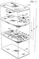
- FIG. 1 shows an exploded perspective view of a personal data card in accordance with the invention.
- Card 10 is a contactless smart card that houses frangible semiconductor chips 200 in a laminated structure that protects them from stress due to flexing and from exposure to external contaminants.
- Semiconductor chips 200 provide the capabilities of a computer within a small portable device.
- Power for the chips is inductively coupled to the coil 500 in the manner disclosed in U.S. Patent 4,802,080 issued to B. J. Bossi et al. on January 31, 1989.
- Bidirectional data transfer is achieved using four capacitors 145 - one pair being used for transmitting data and the other pair being used for receiving data.
- Assembly 8 shown in FIG. 1, comprises circuit board 140 and structural member 130 which are made from the same type of material so that when subjected to changes in temeperature they will shrink or expand at the same rate and thereby avoid warping.
- the card remains generally flat at all temperatures as required by ISO standards.
- structural member 130 is made from heat-stabilized polyester material which is discussed below. Openings 136,137 are created by stamping through-holes in structural member 130. Metallized areas 143- 145 are created on circuit board 140 by etching. These two parts are then joined together in a first lamination process which comprises hearing to 105°C for 13 minutes at 140 PSI. After cooling, components 200, 250, 500 are mounted onto the circuit board 140 through openings 136, 137 in the structural member 130. Assembly 8 is now ready to receive encapsulant materials which enhance the performance and durability of the personal data card 10.
- a slurry of ferrite particles and flexible epoxy is now poured into opening 137 and surrounds wire coil 500. After the slurry cures it remains flexible and operates to enhance the transfer of electrical power to coil 500.
- covers 120 which comprise sheets of cloth that have been impregnated with partially-cured (B-staged) epoxy. Covers 120 are referred to as "Prepreg” which is commercially available from a number of suppliers including the General Electric Company. Assembly 9 is now ready for curing which comprises hearing to 165°C for 45 minutes at 50 PSI. Assembly 9 is frequently referred to as a "smart core" which is suitable for shipping to any one of a number of card issuers.
- label sheets 110, 150 are made from a thermoplastic material and are positioned on the top and bottom surfaces of the card 10 to protect the electronic circuitry and the metallic paths on circuit board 140 from static discharge and external contaminants. It is important that the labels have matching thermal expansion characteristics.
- label sheets 110, 150 are each made from PVC and have a thickness of 0.01 inch (1 mil).
- Each label is subsurface printed and coated with a heat-activated adhesive on one side. The assembled card 10 is then subjected to increased temperature (150° C) and pressure (100 PSI) for a period of rime (10 minutes) in order to activate the adhesive.
- the card issuer typically adds the cover label and embossing in a secure facility to safeguard against card theft and forgery.
- the fully assembled card 10 is now ready for use after suitable programming and testing of semiconductor chips 200 which illustratively comprise a microprocessor and Electrically Erasable and Programmable Read Only Memory (EEPROM).
- EEPROM Electrically Erasable and Programmable Read Only Memory
- Security information such as passwords for accessing certain files, can be entered into the memory of the card at this time also.
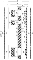
- FIG. 2 is an exploded cross-section view of a preferred embodiment of a personal data card showing the various sheets that cooperate in providing a durable card that meeets ISO standards in a cost-effective manner.
- FIG. 2 also illustrates the approximate relative dimensions of the various sheets. Because the preferred embodiment comprises a contactless card, the top and bottom sheets 110, 150 are without openings so that circuitry within the card receives substantial protection. Greater protection can be achieved by doubling the thickness of sheets 110, 150 to 2 mils each. However, to continue satisfying ISO standards, another of the sheets would need to be decreased in thickness. Heat-activated adhesives 111, 151 are applied to thermoplastic sheets 110, 150 before they are cut to "credit card" size.
- adhesive layer 111 is 2 mils thick while adhesive layer 151 is only 1 mil thick.
- the thickness of adhesive layer 111 is intended to "smooth out” any bumps on the top surface 131 of structural member 130 created by covers 120. These covers serve to protect the encapsulated components within openings 136, 137 of structural member 130.
- Encapsulants 300, 400 are shown removed from through-holes 136, 137 whereas in reality they surround components 200, 500 respectively.
- structural member 130 includes a layer of heat-activated adhesive 133 on the top surface 131 and bottom surface 132 thereof. Such adhesives are dry at room temperature which allows for easy handling. They do not become sticky until sufficient heat is applied.
- adhesive 133 on the bottom surface 132 of the structural member 130 functions to bond the structural member to the top surface 141 of circuit board 140.
- semiconductor chips 200 are bonded to metallized areas 143 on circuit board 140 via wires 220. Such construction has been found to provide highly reliable electrical connections. The chips 200 are placed by machine onto circuit board 140 and are initially held there by an adhesive.
- FIG. 3 represents a perspective view of the assembled personal data card 10 showing illustrative values for the thickness of each sheet.
- At least one semiconductor chip 200 typically a memory chip or the combination of a memory and microprocessor chip, has its undersurface secured to metallized area 142.
- the chip has a plurality of conductive pads 210, usually on top, which are each selectively coupled by a separate one of a set of small diameter wires 220 to a separate one of the metallized pads 143 on the top surface of circuit board 140.
- Each wire typically has a small loop (not shown) near the end thereof connected to the pad 210 on the chip 200 to provide the wire a small degree of strain relief.
- the loop is sized so as to lie below the top of the structural member 130.
- wires 220 are not the only mechanism by which the chip 200 can be electrically connected to circuit board 140. Other well-known techniques, such as tab bonding and flip chip bonding, can also be used for makng electrical connections.
- polyester film having a nominal thickness of 14 mils.
- Certain advantages are associated with the use of polyester that make it an excellent choice for a personal data card. It is a flexible, dielectric material that is less expensive than kapton or polyimide and it embosses better. Further, unlike PVC, it does not become too soft during the high temperature lamination process. For this reason, soldering to a PVC circuit board is not desirable. Polyester films are extruded at relatively high temperatures, and are subject to dimensional change as a function of temperature. The polyester film emerges from an extruding machine in a direction that is known as its machine direction (MD).
- MD machine direction
- the other direction of this generally-planar film is known as its transverse direction (TD).
- TD transverse direction
- a process known as heat-stabilization is employed to reduce the relative rate of thermal expansion in these two directions.
- a typical heat-stabilization process for 14 mil polyester comprises raising the temperature of the polyester film to 150°C for some predetermined rime interval. This process greatly reduces dimensional changes in the polyester material in all directions.
- An acceptable value for shrinkage of the structural member used in the present invention is: MD and TD shrinkage of less than 0.2% unrestrained at 150° C for 30 minutes. So that warpage does not occur, both the structural member and the circuit board are made from similar materials, namely polyester.
- Polyester material is commercially available in different thickness from a number of suppliers. Additionally, it is marketed under various trade names including MYLARTM, PHANEXTM, MELINEXTM - depending on the particular supplier. Polyester material used for the structural (strength) member 130 has a thickness of 0.014 inches (14 mils) which, when coated with 2 mils of heat-activated adhesive on each side, is greater than the height of the semiconductor chip. Thus, the chip does not protrude above the through-hole in the structural member when the circuit board and the structural member are joined.
- polyester refers to any of a group of thermoplastic polyester materials which primarily include, but are not limited to, the polyethylene terephthalate (PET) and the polybutylene terephthalate (PBT) families. In a preferred embodiment of the invention, PET materials are used.
- polyester structural member 130 After the polyester structural member 130 has been heat stabilized, it is coated with a heat-activated adhesive 133 on its top surface 131 and bottom surface 132 (see FIG. 2).
- a suitable adhesive for use on polyester film is A412 which is available from Sheldahl, Inc.
- this adhesive is flame retardant and can be heat sealed with a hot nip roll at about 350°F at 80-100 pli, or platen pressed at 275° - 300° F, 100 - 200 psi for 10 minutes and cooled under pressure to 100° F.
- Circuit board 140 is a composite of a copper foil conductor bonded to the top surface 141 (see FIG. 2) of a polyester film dielectric. Such laminates are frequently used for flexible wiring and interconnects, and are compatible with standard etch processes. A thickness in the polyester material of 0.005 inches (5 mils) is used in the preferred embodiment, although thinner materials (e.g. 3 mils) may be used with acceptable results. Commercially-available materials include the L-5500 Polyester Base Flexible Electrical Laminates from Sheldahl, Inc.
Landscapes
- Engineering & Computer Science (AREA)
- Computer Hardware Design (AREA)
- Microelectronics & Electronic Packaging (AREA)
- Physics & Mathematics (AREA)
- General Physics & Mathematics (AREA)
- Theoretical Computer Science (AREA)
- Credit Cards Or The Like (AREA)
- Structures Or Materials For Encapsulating Or Coating Semiconductor Devices Or Solid State Devices (AREA)
Applications Claiming Priority (2)
| Application Number | Priority Date | Filing Date | Title |
|---|---|---|---|
| US62016690A | 1990-11-30 | 1990-11-30 | |
| US620166 | 1990-11-30 |
Publications (3)
| Publication Number | Publication Date |
|---|---|
| EP0488574A2 true EP0488574A2 (de) | 1992-06-03 |
| EP0488574A3 EP0488574A3 (en) | 1992-11-04 |
| EP0488574B1 EP0488574B1 (de) | 1995-11-08 |
Family
ID=24484856
Family Applications (1)
| Application Number | Title | Priority Date | Filing Date |
|---|---|---|---|
| EP91310677A Expired - Lifetime EP0488574B1 (de) | 1990-11-30 | 1991-11-20 | Aufbau einer Personaldatenkarte |
Country Status (7)
| Country | Link |
|---|---|
| EP (1) | EP0488574B1 (de) |
| JP (1) | JPH04286697A (de) |
| AU (1) | AU627124B2 (de) |
| BR (1) | BR9105051A (de) |
| CA (1) | CA2051836C (de) |
| DE (1) | DE69114451T2 (de) |
| ES (1) | ES2079036T3 (de) |
Cited By (25)
| Publication number | Priority date | Publication date | Assignee | Title |
|---|---|---|---|---|
| GB2279612A (en) * | 1993-07-02 | 1995-01-11 | Gec Avery Ltd | Integrated circuit or smart card. |
| NL9301457A (nl) * | 1993-08-23 | 1995-03-16 | Nedap Nv | Contactloze identificatiekaart of smart card. |
| EP0689165A1 (de) * | 1994-06-22 | 1995-12-27 | SOLAIC (société anonyme) | Kontaktlose Speicherkarte mit IC-Modul |
| WO1998009252A1 (de) * | 1996-08-26 | 1998-03-05 | Tomas Meinen | Verfahren zur herstellung von chipkarten |
| US5822194A (en) * | 1994-03-31 | 1998-10-13 | Ibiden Co., Ltd. | Electronic part mounting device |
| US6207004B1 (en) | 1996-06-17 | 2001-03-27 | Mitsubishi Denki Kabushiki Kaisha | Method for producing thin IC cards and construction thereof |
| RU2171497C2 (ru) * | 1996-11-12 | 2001-07-27 | НАГРА АйДи С.А. | Способ изготовления карт и карты, изготовленные этим способом |
| EP1152368A1 (de) * | 2000-05-05 | 2001-11-07 | Infineon Technologies AG | Chipkarte |
| US6706624B1 (en) * | 2001-10-31 | 2004-03-16 | Lockheed Martin Corporation | Method for making multichip module substrates by encapsulating electrical conductors |
| FR2855890A1 (fr) * | 2003-06-05 | 2004-12-10 | Sagem | Carte multicouche en materiau thermoplastique et procede de securisation de carte multicouche |
| FR2869255A1 (fr) * | 2004-04-27 | 2005-10-28 | Daniel Mignon | Procede pour la realisation de cartes plastiques composites souples et cartes obtenues a l'aide dudit procede. |
| EP1150550A3 (de) * | 2000-04-26 | 2006-01-11 | Audiosmartcard International S.A. | Verfahren zur Verbindung von elektronischen Bausteinen in einer kreditkartenartigen tragbaren Vorrichtung |
| WO2006107968A1 (en) * | 2005-04-06 | 2006-10-12 | Innovatier, Inc. | A smart card and method for manufacturing a smart card |
| US7607249B2 (en) | 2005-07-15 | 2009-10-27 | Innovatier Inc. | RFID bracelet and method for manufacturing a RFID bracelet |
| WO2009142592A1 (en) * | 2008-05-20 | 2009-11-26 | Swecard International Sa | Electronic device and component protection during manufacture |
| US7959085B2 (en) | 2006-04-10 | 2011-06-14 | Innovatier, Inc. | Electronic inlay module used for electronic cards and tags |
| US8727224B2 (en) | 2006-06-20 | 2014-05-20 | Innovatier, Inc. | Embedded electronic device and method for manufacturing an embedded electronic device |
| US9127691B2 (en) | 2010-09-01 | 2015-09-08 | 3M Innovative Properties Company | Compact scroll fan assembly |
| WO2016004002A1 (en) * | 2014-07-01 | 2016-01-07 | Isola Usa Corp. | Prepregs and laminates having a uv curable resin layer |
| US9579868B2 (en) | 2014-07-01 | 2017-02-28 | Isola Usa Corp. | Prepregs and laminates having a UV curable resin layer |
| WO2017048280A1 (en) | 2015-09-18 | 2017-03-23 | X-Card Holdings, Llc | Self-centered inlay and core layer for information carrying card, process and resulting products |
| WO2017162311A1 (en) * | 2016-03-24 | 2017-09-28 | Zwipe As | Method of manufacturing an electronic card |
| GB2579924A (en) * | 2016-10-07 | 2020-07-08 | Jaguar Land Rover Ltd | Control unit |
| US12220897B2 (en) | 2022-10-20 | 2025-02-11 | X-Card Holdings, Llc | Core layer for information carrying card, resulting information carrying card, and methods of making the same |
| US12528279B2 (en) | 2022-10-20 | 2026-01-20 | X-Card Holdings, Llc | Core layer for information carrying card, resulting information carrying card, and methods of making the same |
Families Citing this family (6)
| Publication number | Priority date | Publication date | Assignee | Title |
|---|---|---|---|---|
| JPH07266767A (ja) * | 1994-03-31 | 1995-10-17 | Ibiden Co Ltd | 非接触型icカード及び非接触型icカードの製造方法 |
| CN1079053C (zh) * | 1996-06-17 | 2002-02-13 | 三菱电机株式会社 | 制造薄ic卡的方法及其结构 |
| DE102009016762B4 (de) * | 2009-04-07 | 2016-10-06 | SUMIDA Components & Modules GmbH | Verfahren und Komponentensatz zum Herstellen elektronischer Baugruppen unter Verwendung einer Vergussmasse |
| US8766099B2 (en) | 2009-09-29 | 2014-07-01 | Apple Inc. | Component mounting structures for electronic devices |
| JP2014509269A (ja) * | 2011-01-18 | 2014-04-17 | イノベイティア インコーポレイテッド | 電子装置の製造において電子アセンブリをボトムオーバーレイに取り付ける方法 |
| DE102019118444B4 (de) * | 2019-07-08 | 2021-03-04 | Infineon Technologies Ag | Verfahren zum Herstellen einer Chipkarten-Schichtenstruktur, und Chipkarten-Schichtenstruktur |
Family Cites Families (11)
| Publication number | Priority date | Publication date | Assignee | Title |
|---|---|---|---|---|
| JPS60142489A (ja) * | 1983-12-28 | 1985-07-27 | Dainippon Printing Co Ltd | Icカ−ド |
| JPS61123990A (ja) * | 1984-11-05 | 1986-06-11 | Casio Comput Co Ltd | Icカ−ド |
| JPS61277496A (ja) * | 1985-06-04 | 1986-12-08 | 株式会社東芝 | Icカ−ド |
| JPH0751390B2 (ja) * | 1985-07-10 | 1995-06-05 | カシオ計算機株式会社 | Icカ−ド |
| JPS6282092A (ja) * | 1985-10-07 | 1987-04-15 | カシオ計算機株式会社 | Icカ−ド |
| JPS63149191A (ja) * | 1986-12-15 | 1988-06-21 | 日立マクセル株式会社 | Icカ−ド |
| JPS62276659A (ja) * | 1987-03-31 | 1987-12-01 | Casio Comput Co Ltd | シ−ト状小型電子機器 |
| KR920006339B1 (ko) * | 1988-04-20 | 1992-08-03 | 마쓰시다 덴기 산교 가부시기가이샤 | Ic카드 |
| GB8901189D0 (en) * | 1989-01-19 | 1989-03-15 | Avery W & T Limited | Portable electronic token |
| JPH02204096A (ja) * | 1989-02-03 | 1990-08-14 | Citizen Watch Co Ltd | Icカード製造方法 |
| DE3924439A1 (de) * | 1989-07-24 | 1991-04-18 | Edgar Schneider | Traegerelement mit wenigstens einem integrierten schaltkreis, insbesondere zum einbau in chip-karten, sowie verfahren zur herstellung dieser traegerelemente |
-
1991
- 1991-09-25 CA CA002051836A patent/CA2051836C/en not_active Expired - Fee Related
- 1991-11-20 BR BR919105051A patent/BR9105051A/pt not_active IP Right Cessation
- 1991-11-20 DE DE69114451T patent/DE69114451T2/de not_active Expired - Fee Related
- 1991-11-20 ES ES91310677T patent/ES2079036T3/es not_active Expired - Lifetime
- 1991-11-20 EP EP91310677A patent/EP0488574B1/de not_active Expired - Lifetime
- 1991-11-27 AU AU88219/91A patent/AU627124B2/en not_active Ceased
- 1991-11-29 JP JP3339530A patent/JPH04286697A/ja active Pending
Cited By (44)
| Publication number | Priority date | Publication date | Assignee | Title |
|---|---|---|---|---|
| GB2279612A (en) * | 1993-07-02 | 1995-01-11 | Gec Avery Ltd | Integrated circuit or smart card. |
| NL9301457A (nl) * | 1993-08-23 | 1995-03-16 | Nedap Nv | Contactloze identificatiekaart of smart card. |
| US5822194A (en) * | 1994-03-31 | 1998-10-13 | Ibiden Co., Ltd. | Electronic part mounting device |
| EP0689165A1 (de) * | 1994-06-22 | 1995-12-27 | SOLAIC (société anonyme) | Kontaktlose Speicherkarte mit IC-Modul |
| FR2721732A1 (fr) * | 1994-06-22 | 1995-12-29 | Solaic Sa | Carte à mémoire sans contact dont le circuit électronique comporte un module. |
| US6207004B1 (en) | 1996-06-17 | 2001-03-27 | Mitsubishi Denki Kabushiki Kaisha | Method for producing thin IC cards and construction thereof |
| WO1998009252A1 (de) * | 1996-08-26 | 1998-03-05 | Tomas Meinen | Verfahren zur herstellung von chipkarten |
| RU2171497C2 (ru) * | 1996-11-12 | 2001-07-27 | НАГРА АйДи С.А. | Способ изготовления карт и карты, изготовленные этим способом |
| EP1150550A3 (de) * | 2000-04-26 | 2006-01-11 | Audiosmartcard International S.A. | Verfahren zur Verbindung von elektronischen Bausteinen in einer kreditkartenartigen tragbaren Vorrichtung |
| EP1152368A1 (de) * | 2000-05-05 | 2001-11-07 | Infineon Technologies AG | Chipkarte |
| WO2001086588A1 (de) * | 2000-05-05 | 2001-11-15 | Infineon Technologies Ag | Chipkarte |
| US7269021B2 (en) | 2000-05-05 | 2007-09-11 | Infineon Techonologies Ag | Smart card containing a carrier body for receiving at least one system component having a plurality of electrical components and uniting electrical functions for operating the smart card |
| US6706624B1 (en) * | 2001-10-31 | 2004-03-16 | Lockheed Martin Corporation | Method for making multichip module substrates by encapsulating electrical conductors |
| US7754311B2 (en) | 2003-06-05 | 2010-07-13 | Sagem Securite | Multilayer card of thermoplastic material and a method of making the multilayer card secure |
| FR2855890A1 (fr) * | 2003-06-05 | 2004-12-10 | Sagem | Carte multicouche en materiau thermoplastique et procede de securisation de carte multicouche |
| WO2005004048A1 (fr) * | 2003-06-05 | 2005-01-13 | Sagem Defense Securite | Carte multicouche en materiau thermoplastique et procede de securisation de carte multicouche |
| FR2869255A1 (fr) * | 2004-04-27 | 2005-10-28 | Daniel Mignon | Procede pour la realisation de cartes plastiques composites souples et cartes obtenues a l'aide dudit procede. |
| EP1591238A1 (de) * | 2004-04-27 | 2005-11-02 | Daniel Mignon | Verfahren zur Herstellung von flexiblen Verbundkunststoffkarten und so hergestellte Karten |
| WO2006107968A1 (en) * | 2005-04-06 | 2006-10-12 | Innovatier, Inc. | A smart card and method for manufacturing a smart card |
| US7237724B2 (en) * | 2005-04-06 | 2007-07-03 | Robert Singleton | Smart card and method for manufacturing a smart card |
| CN100595784C (zh) * | 2005-04-06 | 2010-03-24 | 因诺瓦蒂尔公司 | 一种智能卡的制造方法 |
| US7607249B2 (en) | 2005-07-15 | 2009-10-27 | Innovatier Inc. | RFID bracelet and method for manufacturing a RFID bracelet |
| US7959085B2 (en) | 2006-04-10 | 2011-06-14 | Innovatier, Inc. | Electronic inlay module used for electronic cards and tags |
| US8727224B2 (en) | 2006-06-20 | 2014-05-20 | Innovatier, Inc. | Embedded electronic device and method for manufacturing an embedded electronic device |
| WO2009142592A1 (en) * | 2008-05-20 | 2009-11-26 | Swecard International Sa | Electronic device and component protection during manufacture |
| US9481424B2 (en) | 2010-09-01 | 2016-11-01 | 3M Innovative Properties Company | Compact scroll fan assembly |
| US9127691B2 (en) | 2010-09-01 | 2015-09-08 | 3M Innovative Properties Company | Compact scroll fan assembly |
| US9579868B2 (en) | 2014-07-01 | 2017-02-28 | Isola Usa Corp. | Prepregs and laminates having a UV curable resin layer |
| US10631412B2 (en) | 2014-07-01 | 2020-04-21 | Isola Usa Corp. | Prepregs and laminates having a UV curable resin layer |
| US12336103B2 (en) | 2014-07-01 | 2025-06-17 | Isola Usa Corp. | Prepregs and laminates having a UV curable resin layer |
| US11558962B2 (en) | 2014-07-01 | 2023-01-17 | Isola Usa Corp. | Prepregs and laminates having a UV curable resin layer |
| WO2016004002A1 (en) * | 2014-07-01 | 2016-01-07 | Isola Usa Corp. | Prepregs and laminates having a uv curable resin layer |
| US10839280B2 (en) | 2015-09-18 | 2020-11-17 | X-Card Holdings, Llc | Self-centered inlay and core layer for information carrying card, process and resulting products |
| US10339434B2 (en) | 2015-09-18 | 2019-07-02 | X-Card Holdings, Llc | Self-centered inlay and core layer for information carrying card, process and resulting products |
| EP3350750A4 (de) * | 2015-09-18 | 2019-04-10 | X-Card Holdings, LLC | Selbstzentrierte einlagen- und kernschicht für informationstragende karte, verfahren und resultierende produkte |
| CN108027892A (zh) * | 2015-09-18 | 2018-05-11 | X卡控股有限公司 | 用于信息携带卡的自定心嵌体和芯层、过程以及得到的产品 |
| CN108027892B (zh) * | 2015-09-18 | 2021-04-09 | X卡控股有限公司 | 用于信息携带卡的自定心嵌体和芯层、过程以及得到的产品 |
| WO2017048280A1 (en) | 2015-09-18 | 2017-03-23 | X-Card Holdings, Llc | Self-centered inlay and core layer for information carrying card, process and resulting products |
| US12340266B2 (en) | 2015-09-18 | 2025-06-24 | X-Card Holdings, Llc | Self-centered inlay and core layer for information carrying card, process and resulting products |
| WO2017162311A1 (en) * | 2016-03-24 | 2017-09-28 | Zwipe As | Method of manufacturing an electronic card |
| GB2579924A (en) * | 2016-10-07 | 2020-07-08 | Jaguar Land Rover Ltd | Control unit |
| GB2579924B (en) * | 2016-10-07 | 2021-03-03 | Jaguar Land Rover Ltd | Control unit |
| US12220897B2 (en) | 2022-10-20 | 2025-02-11 | X-Card Holdings, Llc | Core layer for information carrying card, resulting information carrying card, and methods of making the same |
| US12528279B2 (en) | 2022-10-20 | 2026-01-20 | X-Card Holdings, Llc | Core layer for information carrying card, resulting information carrying card, and methods of making the same |
Also Published As
| Publication number | Publication date |
|---|---|
| EP0488574B1 (de) | 1995-11-08 |
| JPH04286697A (ja) | 1992-10-12 |
| CA2051836C (en) | 1996-07-23 |
| BR9105051A (pt) | 1992-06-23 |
| ES2079036T3 (es) | 1996-01-01 |
| AU8821991A (en) | 1992-06-18 |
| AU627124B2 (en) | 1992-08-13 |
| DE69114451D1 (de) | 1995-12-14 |
| EP0488574A3 (en) | 1992-11-04 |
| CA2051836A1 (en) | 1992-05-31 |
| DE69114451T2 (de) | 1996-03-21 |
Similar Documents
| Publication | Publication Date | Title |
|---|---|---|
| EP0488574B1 (de) | Aufbau einer Personaldatenkarte | |
| JP2757309B2 (ja) | Icカードの構造 | |
| EP0163534B1 (de) | Karte mit IC-Baustein und Verfahren zur Herstellung derselben | |
| EP0952542B1 (de) | Ic modul und ic karte | |
| JP4268681B2 (ja) | Icカード | |
| US20090095415A1 (en) | Reinforced radio frequency identification device support and its manufacturing method | |
| US20110011939A1 (en) | Contact-less and dual interface inlays and methods for producing the same | |
| US20010055202A1 (en) | Reinforced micromodule | |
| US8864040B2 (en) | Method of fabricating a microcircuit device | |
| US10157848B2 (en) | Chip card module arrangement, chip card arrangement and method for producing a chip card arrangement | |
| CN101385402A (zh) | 电路基板以及电路基板的制造方法 | |
| US20240013021A1 (en) | Card with fingerprint biometrics | |
| US6031724A (en) | IC card and method of manufacturing the same | |
| US6521985B1 (en) | Method for the production of a portable integrated circuit electronic device comprising a low-cost dielectric | |
| JPH11345299A (ja) | 非接触型icカード及びその製造方法 | |
| KR19990076679A (ko) | 비접촉식 기술에서 사용하기 위한 칩카드의 제조방법 | |
| CN117015782A (zh) | 多个芯片卡模块的制造方法以及支承该多个模块的柔性材料带 | |
| EP0463871A2 (de) | Wertkarte mit integrierter Schaltung | |
| KR100363657B1 (ko) | 집적회로칩카드 및 이의 제조방법 | |
| JP3769332B2 (ja) | Icカードの製造方法 | |
| JPH11345297A (ja) | データキャリア及びその製造方法 | |
| JPH11250209A (ja) | 非接触型icカード | |
| JP2000048151A (ja) | 非接触icカード | |
| JP7831180B2 (ja) | Icカード | |
| CN114175258A (zh) | 封装电子模块及其制造方法 |
Legal Events
| Date | Code | Title | Description |
|---|---|---|---|
| PUAI | Public reference made under article 153(3) epc to a published international application that has entered the european phase |
Free format text: ORIGINAL CODE: 0009012 |
|
| AK | Designated contracting states |
Kind code of ref document: A2 Designated state(s): DE ES FR GB IT |
|
| PUAL | Search report despatched |
Free format text: ORIGINAL CODE: 0009013 |
|
| AK | Designated contracting states |
Kind code of ref document: A3 Designated state(s): DE ES FR GB IT |
|
| 17P | Request for examination filed |
Effective date: 19930422 |
|
| RAP3 | Party data changed (applicant data changed or rights of an application transferred) |
Owner name: AT&T CORP. |
|
| 17Q | First examination report despatched |
Effective date: 19940831 |
|
| GRAA | (expected) grant |
Free format text: ORIGINAL CODE: 0009210 |
|
| AK | Designated contracting states |
Kind code of ref document: B1 Designated state(s): DE ES FR GB IT |
|
| ITF | It: translation for a ep patent filed | ||
| ET | Fr: translation filed | ||
| REF | Corresponds to: |
Ref document number: 69114451 Country of ref document: DE Date of ref document: 19951214 |
|
| REG | Reference to a national code |
Ref country code: ES Ref legal event code: FG2A Ref document number: 2079036 Country of ref document: ES Kind code of ref document: T3 |
|
| PLBE | No opposition filed within time limit |
Free format text: ORIGINAL CODE: 0009261 |
|
| STAA | Information on the status of an ep patent application or granted ep patent |
Free format text: STATUS: NO OPPOSITION FILED WITHIN TIME LIMIT |
|
| 26N | No opposition filed | ||
| REG | Reference to a national code |
Ref country code: GB Ref legal event code: IF02 |
|
| PGFP | Annual fee paid to national office [announced via postgrant information from national office to epo] |
Ref country code: ES Payment date: 20071129 Year of fee payment: 17 Ref country code: DE Payment date: 20071123 Year of fee payment: 17 |
|
| PGFP | Annual fee paid to national office [announced via postgrant information from national office to epo] |
Ref country code: IT Payment date: 20071126 Year of fee payment: 17 |
|
| PGFP | Annual fee paid to national office [announced via postgrant information from national office to epo] |
Ref country code: GB Payment date: 20071120 Year of fee payment: 17 Ref country code: FR Payment date: 20071122 Year of fee payment: 17 |
|
| GBPC | Gb: european patent ceased through non-payment of renewal fee |
Effective date: 20081120 |
|
| PG25 | Lapsed in a contracting state [announced via postgrant information from national office to epo] |
Ref country code: IT Free format text: LAPSE BECAUSE OF NON-PAYMENT OF DUE FEES Effective date: 20081120 |
|
| REG | Reference to a national code |
Ref country code: FR Ref legal event code: ST Effective date: 20090731 |
|
| PG25 | Lapsed in a contracting state [announced via postgrant information from national office to epo] |
Ref country code: DE Free format text: LAPSE BECAUSE OF NON-PAYMENT OF DUE FEES Effective date: 20090603 |
|
| PG25 | Lapsed in a contracting state [announced via postgrant information from national office to epo] |
Ref country code: GB Free format text: LAPSE BECAUSE OF NON-PAYMENT OF DUE FEES Effective date: 20081120 |
|
| REG | Reference to a national code |
Ref country code: ES Ref legal event code: FD2A Effective date: 20081121 |
|
| PG25 | Lapsed in a contracting state [announced via postgrant information from national office to epo] |
Ref country code: ES Free format text: LAPSE BECAUSE OF NON-PAYMENT OF DUE FEES Effective date: 20081121 |
|
| PG25 | Lapsed in a contracting state [announced via postgrant information from national office to epo] |
Ref country code: FR Free format text: LAPSE BECAUSE OF NON-PAYMENT OF DUE FEES Effective date: 20081130 |