EP0689165A1 - Kontaktlose Speicherkarte mit IC-Modul - Google Patents
Kontaktlose Speicherkarte mit IC-Modul Download PDFInfo
- Publication number
- EP0689165A1 EP0689165A1 EP95401458A EP95401458A EP0689165A1 EP 0689165 A1 EP0689165 A1 EP 0689165A1 EP 95401458 A EP95401458 A EP 95401458A EP 95401458 A EP95401458 A EP 95401458A EP 0689165 A1 EP0689165 A1 EP 0689165A1
- Authority
- EP
- European Patent Office
- Prior art keywords
- module
- insulating
- memory card
- printed circuit
- insulating support
- Prior art date
- Legal status (The legal status is an assumption and is not a legal conclusion. Google has not performed a legal analysis and makes no representation as to the accuracy of the status listed.)
- Granted
Links
Images

Classifications
-
- G—PHYSICS
- G06—COMPUTING OR CALCULATING; COUNTING
- G06K—GRAPHICAL DATA READING; PRESENTATION OF DATA; RECORD CARRIERS; HANDLING RECORD CARRIERS
- G06K19/00—Record carriers for use with machines and with at least a part designed to carry digital markings
- G06K19/06—Record carriers for use with machines and with at least a part designed to carry digital markings characterised by the kind of the digital marking, e.g. shape, nature, code
- G06K19/067—Record carriers with conductive marks, printed circuits or semiconductor circuit elements, e.g. credit or identity cards also with resonating or responding marks without active components
- G06K19/07—Record carriers with conductive marks, printed circuits or semiconductor circuit elements, e.g. credit or identity cards also with resonating or responding marks without active components with integrated circuit chips
- G06K19/077—Constructional details, e.g. mounting of circuits in the carrier
- G06K19/07749—Constructional details, e.g. mounting of circuits in the carrier the record carrier being capable of non-contact communication, e.g. constructional details of the antenna of a non-contact smart card
- G06K19/0775—Constructional details, e.g. mounting of circuits in the carrier the record carrier being capable of non-contact communication, e.g. constructional details of the antenna of a non-contact smart card arrangements for connecting the integrated circuit to the antenna
-
- G—PHYSICS
- G06—COMPUTING OR CALCULATING; COUNTING
- G06K—GRAPHICAL DATA READING; PRESENTATION OF DATA; RECORD CARRIERS; HANDLING RECORD CARRIERS
- G06K19/00—Record carriers for use with machines and with at least a part designed to carry digital markings
- G06K19/06—Record carriers for use with machines and with at least a part designed to carry digital markings characterised by the kind of the digital marking, e.g. shape, nature, code
- G06K19/067—Record carriers with conductive marks, printed circuits or semiconductor circuit elements, e.g. credit or identity cards also with resonating or responding marks without active components
- G06K19/07—Record carriers with conductive marks, printed circuits or semiconductor circuit elements, e.g. credit or identity cards also with resonating or responding marks without active components with integrated circuit chips
- G06K19/077—Constructional details, e.g. mounting of circuits in the carrier
- G06K19/07749—Constructional details, e.g. mounting of circuits in the carrier the record carrier being capable of non-contact communication, e.g. constructional details of the antenna of a non-contact smart card
-
- H—ELECTRICITY
- H05—ELECTRIC TECHNIQUES NOT OTHERWISE PROVIDED FOR
- H05K—PRINTED CIRCUITS; CASINGS OR CONSTRUCTIONAL DETAILS OF ELECTRIC APPARATUS; MANUFACTURE OF ASSEMBLAGES OF ELECTRICAL COMPONENTS
- H05K3/00—Apparatus or processes for manufacturing printed circuits
- H05K3/30—Assembling printed circuits with electric components, e.g. with resistors
- H05K3/32—Assembling printed circuits with electric components, e.g. with resistors electrically connecting electric components or wires to printed circuits
- H05K3/34—Assembling printed circuits with electric components, e.g. with resistors electrically connecting electric components or wires to printed circuits by soldering
- H05K3/341—Surface mounted components
- H05K3/3431—Leadless components
-
- H—ELECTRICITY
- H10—SEMICONDUCTOR DEVICES; ELECTRIC SOLID-STATE DEVICES NOT OTHERWISE PROVIDED FOR
- H10W—GENERIC PACKAGES, INTERCONNECTIONS, CONNECTORS OR OTHER CONSTRUCTIONAL DETAILS OF DEVICES COVERED BY CLASS H10
- H10W90/00—Package configurations
- H10W90/701—Package configurations characterised by the relative positions of pads or connectors relative to package parts
- H10W90/751—Package configurations characterised by the relative positions of pads or connectors relative to package parts of bond wires
- H10W90/754—Package configurations characterised by the relative positions of pads or connectors relative to package parts of bond wires between a chip and a stacked insulating package substrate, interposer or RDL
Definitions
- the present invention relates to a contactless memory card provided with an electronic circuit physically inaccessible from the outside and comprising, on an insulating film, electronic components connected by conductive elements.
- the present invention proposes to provide a solution to this problem and, to do this, it relates to a contactless memory card having the constitution mentioned above and which is characterized in that at least one of the components of the electronic circuit is constituted by a module comprising an insulating support provided with holes, a printed circuit located on one of the faces of the insulating support, an integrated circuit located on the side of the other face of the insulating support and electrically connected to the printed circuit by conductive wires passing through holes in the insulating support, and an insulating protective material coating the integrated circuit and the conductive wires, the printed circuit of this module being retained by a conductive material against the conductive elements carried by the insulating film.
- the module used in the contactless memory card according to the invention is a semi-finished product of the type of those which are produced in very large series and at high rate for conventional memory cards whose contacts are visible.
- the module must be fixed against the conductive elements of the insulating film in a precise predetermined position so that the memory card can function properly.
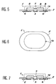
- the present invention provides that the module includes a mark on its face opposite the printed circuit.
- the module can be correctly placed on the insulating film without the slightest trial and error, which makes it possible to increase the production rates of the cards.
- the mark consists of at least one hole made in the insulating support, this hole being able to be closed by the printed circuit.
- the contactless memory card according to the invention is further characterized in that the insulating film is provided, on its face carrying the electronic components, with a layer of insulating material covering the latter, this layer perfectly protecting the electronic circuit against external aggressions.
- the other face of the insulating film can also be provided with a second layer of insulating material.
- the module 1 that can be seen in Figures 1 to 3 includes an insulating support 2 provided with a central hole 3 and peripheral holes 4, a printed circuit consisting of a central conductive element 5 and lateral conductive elements 6 carried by one of the faces of the insulating support 2, an integrated circuit 7 fixed on the central conductive element 5, on the side of the central hole 3, and electrically connected to the lateral conductive elements 6 by conductive wires 8 passing through the peripheral holes 4, and an insulating protective material 9 coating the integrated circuit 7 and the conducting wires 8.
- the insulating support 2 is made of plastic, preferably polyimide or epoxy reinforced with glass fibers.
- the conductors 5 and 6 of the printed circuit can for their part be produced for example by etching or electrolytic deposition of metal layers, or by deposition by screen printing of a conductive ink.
- the lateral conductive elements 6 are connected, by means of a conductive adhesive 10, to conductive elements 11 deposited on one of the faces of an insulating film 12 and which, like the module 1, are part of the electronic circuit of the contactless memory card shown in partial and schematic section in FIG. 4.
- the electronic circuit of this card includes a certain number of electronic components (not shown) other than the module 1, these components can for example consist of capacitors, resistors, antennas, etc.
- the body of the card consists of two layers of insulating plastic material 13,14 fixed respectively against the two faces of the insulating film 12.
- the module 1 can be quickly fixed in the appropriate position against the conductive elements 11 when it is stored with its printed circuit facing upwards.
- the operator can indeed use one of the conductive elements 5,6 of the printed circuit as a reference to identify without hesitation the position in which he must fix the module against the conductive elements.
- the insulating support 2 of the module can be provided with one or more holes 15, one end of which is closed off by one of the conductive elements 6 of the printed circuit, as shown in FIG. 5.
- the support 2 and one of the conductive elements 6 can be provided with a bore 16, as shown in FIG. 7.
- the fixing of the module 1 against the conductive elements 11 could be automated, the installation used being able advantageously to include detection means capable of locating a particular conductive element of the printed circuit, or the hole 15 or 16 produced in the insulating support 2.
Landscapes
- Engineering & Computer Science (AREA)
- Microelectronics & Electronic Packaging (AREA)
- Computer Hardware Design (AREA)
- Physics & Mathematics (AREA)
- General Physics & Mathematics (AREA)
- Theoretical Computer Science (AREA)
- Credit Cards Or The Like (AREA)
- Coupling Device And Connection With Printed Circuit (AREA)
Applications Claiming Priority (2)
| Application Number | Priority Date | Filing Date | Title |
|---|---|---|---|
| FR9407657A FR2721732B1 (fr) | 1994-06-22 | 1994-06-22 | Carte à mémoire sans contact dont le circuit électronique comporte un module. |
| FR9407657 | 1994-06-22 |
Publications (3)
| Publication Number | Publication Date |
|---|---|
| EP0689165A1 true EP0689165A1 (de) | 1995-12-27 |
| EP0689165B1 EP0689165B1 (de) | 1999-02-24 |
| EP0689165B2 EP0689165B2 (de) | 2003-01-29 |
Family
ID=9464513
Family Applications (1)
| Application Number | Title | Priority Date | Filing Date |
|---|---|---|---|
| EP95401458A Expired - Lifetime EP0689165B2 (de) | 1994-06-22 | 1995-06-20 | Kontaktlose Speicherkarte mit IC-Modul |
Country Status (6)
| Country | Link |
|---|---|
| US (1) | US5640306A (de) |
| EP (1) | EP0689165B2 (de) |
| JP (1) | JPH0855206A (de) |
| AT (1) | ATE176959T1 (de) |
| DE (1) | DE69507915T3 (de) |
| FR (1) | FR2721732B1 (de) |
Cited By (2)
| Publication number | Priority date | Publication date | Assignee | Title |
|---|---|---|---|---|
| WO1997034247A3 (de) * | 1996-03-14 | 1998-01-08 | Pav Card Gmbh | Chipkarte, verbindungsanordnung und verfahren zum herstellen einer chipkarte |
| WO1998008191A1 (de) * | 1996-08-22 | 1998-02-26 | Pav Card Gmbh | Verfahren zur herstellung einer elektrischen und mechanischen verbindung eines moduls in einer ausnehmung eines kartenträgers |
Families Citing this family (23)
| Publication number | Priority date | Publication date | Assignee | Title |
|---|---|---|---|---|
| DE4431604A1 (de) * | 1994-09-05 | 1996-03-07 | Siemens Ag | Schaltungsanordnung mit einem Chipkartenmodul und einer damit verbundenen Spule |
| FR2734983B1 (fr) | 1995-05-29 | 1997-07-04 | Sgs Thomson Microelectronics | Utilisation d'un micromodule comme boitier de montage en surface et procede correspondant |
| AT1470U1 (de) * | 1995-08-01 | 1997-05-26 | Austria Card | Laminierte karte und verfahren zu ihrer herstellung |
| JPH0944576A (ja) * | 1995-08-02 | 1997-02-14 | Hitachi Ltd | 電子財布貸付システム |
| DE19528730A1 (de) * | 1995-08-04 | 1997-02-06 | Giesecke & Devrient Gmbh | Verfahren zur Herstellung eines Datenträgers |
| FR2741191B1 (fr) * | 1995-11-14 | 1998-01-09 | Sgs Thomson Microelectronics | Procede de fabrication d'un micromodule, notamment pour cartes a puces |
| US5892661A (en) * | 1996-10-31 | 1999-04-06 | Motorola, Inc. | Smartcard and method of making |
| FR2769390B1 (fr) * | 1997-10-08 | 2003-02-14 | Gemplus Card Int | Procede de fabrication de cartes a puce aptes a assurer un fonctionnement a contact et sans contact, et de cartes a puce sans contact |
| US6651891B1 (en) * | 1997-11-04 | 2003-11-25 | Elke Zakel | Method for producing contactless chip cards and corresponding contactless chip card |
| FR2778997B1 (fr) * | 1998-05-20 | 2000-06-23 | Bull Cp8 | Support pour un circuit electronique, comprenant des moyens anti-arrachement |
| US6297789B2 (en) | 1998-07-09 | 2001-10-02 | Tyco Electronics Corporation | Integrated circuit card with liquid crystal display for viewing at least a portion of the information stored in the card |
| DE29824520U1 (de) * | 1998-09-10 | 2001-06-28 | Skidata Ag, Gartenau | Kartenförmiger Datenträger |
| US6337836B1 (en) | 1999-06-01 | 2002-01-08 | Arthur F. Eidelson | Programmable electronic label |
| US6362972B1 (en) | 2000-04-13 | 2002-03-26 | Molex Incorporated | Contactless interconnection system |
| US6612852B1 (en) * | 2000-04-13 | 2003-09-02 | Molex Incorporated | Contactless interconnection system |
| US6588660B1 (en) | 2000-09-29 | 2003-07-08 | Hewlett-Packard Development Company, L.P. | Passive contactless smartcard security system |
| EP1942391B1 (de) | 2001-03-28 | 2017-01-18 | Irdeto B.V. | Computerlesbare Mediumvorrichtung und Verfahren zum Abspielen von verschlüsselten digitalen Videos |
| KR20030076274A (ko) * | 2002-03-18 | 2003-09-26 | 도레 엔지니아린구 가부시키가이샤 | 비접촉 아이디 카드류 및 그 제조방법 |
| US7094633B2 (en) * | 2003-06-23 | 2006-08-22 | Sandisk Corporation | Method for efficiently producing removable peripheral cards |
| EP1642206B1 (de) | 2003-07-07 | 2017-12-20 | Irdeto B.V. | Umprogrammierbare sicherheit zur kontrolle von widerrechtlichen kopien und zur ermöglichung eines interaktiven inhalts |
| KR100723493B1 (ko) * | 2005-07-18 | 2007-06-04 | 삼성전자주식회사 | 와이어 본딩 및 플립 칩 본딩이 가능한 스마트 카드 모듈기판 및 이를 포함하는 스마트 카드 모듈 |
| JP6090006B2 (ja) * | 2013-06-25 | 2017-03-08 | 凸版印刷株式会社 | Icモジュール、デュアルicカードおよびicモジュールの製造方法 |
| US10737933B2 (en) * | 2016-04-05 | 2020-08-11 | University Of Florida Research Foundation, Incorporated | Flush-mount micromachined transducers |
Citations (4)
| Publication number | Priority date | Publication date | Assignee | Title |
|---|---|---|---|---|
| EP0094716A1 (de) * | 1982-05-14 | 1983-11-23 | Rtc-Compelec | Verfahren zur Verbindung eines Halbleiters mit Elementen eines Trägers, insbesondere einer tragbaren Karte |
| EP0116148A1 (de) * | 1982-12-28 | 1984-08-22 | GAO Gesellschaft für Automation und Organisation mbH | Ausweiskarte mit integriertem Schaltkreis |
| EP0488574A2 (de) * | 1990-11-30 | 1992-06-03 | AT&T Corp. | Aufbau einer Personaldatenkarte |
| FR2686996A1 (fr) * | 1992-01-31 | 1993-08-06 | Solaic Sa | Procede de fabrication d'une carte a memoire comprenant un micromodule equipe d'un capot, et carte a memoire ainsi obtenue. |
Family Cites Families (5)
| Publication number | Priority date | Publication date | Assignee | Title |
|---|---|---|---|---|
| JPS61137335A (ja) * | 1984-12-10 | 1986-06-25 | Toshiba Corp | 半導体装置 |
| DE3723547C2 (de) * | 1987-07-16 | 1996-09-26 | Gao Ges Automation Org | Trägerelement zum Einbau in Ausweiskarten |
| JPH0687486B2 (ja) * | 1989-10-25 | 1994-11-02 | 三菱電機株式会社 | Icカード用モジュール |
| US5148266A (en) * | 1990-09-24 | 1992-09-15 | Ist Associates, Inc. | Semiconductor chip assemblies having interposer and flexible lead |
| DE4416697A1 (de) † | 1994-05-11 | 1995-11-16 | Giesecke & Devrient Gmbh | Datenträger mit integriertem Schaltkreis |
-
1994
- 1994-06-22 FR FR9407657A patent/FR2721732B1/fr not_active Expired - Fee Related
-
1995
- 1995-06-20 US US08/492,483 patent/US5640306A/en not_active Expired - Lifetime
- 1995-06-20 AT AT95401458T patent/ATE176959T1/de not_active IP Right Cessation
- 1995-06-20 JP JP7153530A patent/JPH0855206A/ja active Pending
- 1995-06-20 EP EP95401458A patent/EP0689165B2/de not_active Expired - Lifetime
- 1995-06-20 DE DE69507915T patent/DE69507915T3/de not_active Expired - Fee Related
Patent Citations (4)
| Publication number | Priority date | Publication date | Assignee | Title |
|---|---|---|---|---|
| EP0094716A1 (de) * | 1982-05-14 | 1983-11-23 | Rtc-Compelec | Verfahren zur Verbindung eines Halbleiters mit Elementen eines Trägers, insbesondere einer tragbaren Karte |
| EP0116148A1 (de) * | 1982-12-28 | 1984-08-22 | GAO Gesellschaft für Automation und Organisation mbH | Ausweiskarte mit integriertem Schaltkreis |
| EP0488574A2 (de) * | 1990-11-30 | 1992-06-03 | AT&T Corp. | Aufbau einer Personaldatenkarte |
| FR2686996A1 (fr) * | 1992-01-31 | 1993-08-06 | Solaic Sa | Procede de fabrication d'une carte a memoire comprenant un micromodule equipe d'un capot, et carte a memoire ainsi obtenue. |
Cited By (2)
| Publication number | Priority date | Publication date | Assignee | Title |
|---|---|---|---|---|
| WO1997034247A3 (de) * | 1996-03-14 | 1998-01-08 | Pav Card Gmbh | Chipkarte, verbindungsanordnung und verfahren zum herstellen einer chipkarte |
| WO1998008191A1 (de) * | 1996-08-22 | 1998-02-26 | Pav Card Gmbh | Verfahren zur herstellung einer elektrischen und mechanischen verbindung eines moduls in einer ausnehmung eines kartenträgers |
Also Published As
| Publication number | Publication date |
|---|---|
| DE69507915T2 (de) | 1999-08-12 |
| ATE176959T1 (de) | 1999-03-15 |
| EP0689165B2 (de) | 2003-01-29 |
| DE69507915D1 (de) | 1999-04-01 |
| FR2721732A1 (fr) | 1995-12-29 |
| DE69507915T3 (de) | 2003-11-13 |
| US5640306A (en) | 1997-06-17 |
| FR2721732B1 (fr) | 1996-08-30 |
| EP0689165B1 (de) | 1999-02-24 |
| JPH0855206A (ja) | 1996-02-27 |
Similar Documents
| Publication | Publication Date | Title |
|---|---|---|
| EP0689165B1 (de) | Kontaktlose Speicherkarte mit IC-Modul | |
| FR2787640A1 (fr) | Agencement d'une antenne dans un environnement metallique | |
| CH672870B5 (de) | ||
| FR2631200A1 (fr) | Circuit imprime souple, notamment pour carte a microcircuits electroniques, et carte incorporant un tel circuit | |
| EP0239069B1 (de) | Streifenleitungsantennengruppe | |
| EP1240619A1 (de) | Elektronisches etikett | |
| FR2925749A1 (fr) | Appareil a moyens de reglage sans contact | |
| FR3000833A1 (fr) | Cable dote d'un moyen d'identification ameliore | |
| EP3408799A1 (de) | Verfahren zur herstellung eines chipkartenmoduls und chipkarte | |
| EP3059698B1 (de) | Herstellungsverfahren eines einseitigen elektronischen Moduls, das Verbindungszonen umfasst | |
| EP1431847B1 (de) | Tragbares elektronisches Gerät, insbesondere Uhr, mit einer Antenne, die aus einer Spule mit grossem Diameter gebildet ist | |
| FR2771834A1 (fr) | Dispositif de connexion electrique pour cooperer avec un support electronique mobile | |
| FR2662896A1 (fr) | Substrat de montage de composants electriques. | |
| EP1552471B1 (de) | Transponder und werkzeug zum lesen und/oder schreiben von daten in den transponder | |
| EP2915093B1 (de) | Sicherer verbinder für eine speicherkarte | |
| EP3391460A1 (de) | Einseitiges antennenmodul mit cms-vorrichtung | |
| WO2015165803A2 (fr) | Système de fermeture/ouverture de bracelet réalisant une fonction électrique | |
| EP1532579B1 (de) | Elektronische label-antenne | |
| EP0996930A1 (de) | Unterlage für elektrische schaltanordnung mit mitteln die entkoppeln vermeiden | |
| EP3020068B1 (de) | Elektronisches modul und verfahren zur herstellung davon | |
| EP0346228A1 (de) | Maskenplatte für eine gedruckte Schaltungskarte und Verfahren zur Herstellung | |
| EP4162238B1 (de) | Elektronisches messgerät mit elektrode | |
| EP0360647A1 (de) | Kodiervorrichtung, insbesondere für Leiterplatten | |
| FR2862413A1 (fr) | Capteur de mesure a liaisons conductrices sans raideur et procede de fabrication | |
| WO2001004988A1 (fr) | Antenne pour cartes a puce sans contact, cartes hybrides et etiquettes electroniques |
Legal Events
| Date | Code | Title | Description |
|---|---|---|---|
| PUAI | Public reference made under article 153(3) epc to a published international application that has entered the european phase |
Free format text: ORIGINAL CODE: 0009012 |
|
| AK | Designated contracting states |
Kind code of ref document: A1 Designated state(s): AT BE CH DE DK ES GB GR IE IT LI LU MC NL PT SE |
|
| RAX | Requested extension states of the european patent have changed |
Free format text: LT PAYMENT 950623;SI PAYMENT 950623 |
|
| 17P | Request for examination filed |
Effective date: 19960117 |
|
| GRAG | Despatch of communication of intention to grant |
Free format text: ORIGINAL CODE: EPIDOS AGRA |
|
| GRAG | Despatch of communication of intention to grant |
Free format text: ORIGINAL CODE: EPIDOS AGRA |
|
| 17Q | First examination report despatched |
Effective date: 19980623 |
|
| GRAG | Despatch of communication of intention to grant |
Free format text: ORIGINAL CODE: EPIDOS AGRA |
|
| GRAH | Despatch of communication of intention to grant a patent |
Free format text: ORIGINAL CODE: EPIDOS IGRA |
|
| GRAH | Despatch of communication of intention to grant a patent |
Free format text: ORIGINAL CODE: EPIDOS IGRA |
|
| GRAA | (expected) grant |
Free format text: ORIGINAL CODE: 0009210 |
|
| AK | Designated contracting states |
Kind code of ref document: B1 Designated state(s): AT BE CH DE DK ES GB GR IE IT LI LU MC NL PT SE |
|
| AX | Request for extension of the european patent |
Free format text: LT PAYMENT 950623;SI PAYMENT 950623 |
|
| LTIE | Lt: invalidation of european patent or patent extension | ||
| PG25 | Lapsed in a contracting state [announced via postgrant information from national office to epo] |
Ref country code: SE Free format text: THE PATENT HAS BEEN ANNULLED BY A DECISION OF A NATIONAL AUTHORITY Effective date: 19990224 Ref country code: NL Free format text: LAPSE BECAUSE OF FAILURE TO SUBMIT A TRANSLATION OF THE DESCRIPTION OR TO PAY THE FEE WITHIN THE PRESCRIBED TIME-LIMIT Effective date: 19990224 Ref country code: IT Free format text: LAPSE BECAUSE OF FAILURE TO SUBMIT A TRANSLATION OF THE DESCRIPTION OR TO PAY THE FEE WITHIN THE PRE;WARNING: LAPSES OF ITALIAN PATENTS WITH EFFECTIVE DATE BEFORE 2007 MAY HAVE OCCURRED AT ANY TIME BEFORE 2007. THE CORRECT EFFECTIVE DATE MAY BE DIFFERENT FROM THE ONE RECORDED.SCRIBED TIME-LIMIT Effective date: 19990224 Ref country code: GR Free format text: LAPSE BECAUSE OF NON-PAYMENT OF DUE FEES Effective date: 19990224 Ref country code: ES Free format text: THE PATENT HAS BEEN ANNULLED BY A DECISION OF A NATIONAL AUTHORITY Effective date: 19990224 Ref country code: AT Free format text: LAPSE BECAUSE OF FAILURE TO SUBMIT A TRANSLATION OF THE DESCRIPTION OR TO PAY THE FEE WITHIN THE PRESCRIBED TIME-LIMIT Effective date: 19990224 |
|
| REF | Corresponds to: |
Ref document number: 176959 Country of ref document: AT Date of ref document: 19990315 Kind code of ref document: T |
|
| REG | Reference to a national code |
Ref country code: CH Ref legal event code: EP |
|
| RAP2 | Party data changed (patent owner data changed or rights of a patent transferred) |
Owner name: SCHLUMBERGER SYSTEMES |
|
| REG | Reference to a national code |
Ref country code: IE Ref legal event code: FG4D Free format text: FRENCH |
|
| REF | Corresponds to: |
Ref document number: 69507915 Country of ref document: DE Date of ref document: 19990401 |
|
| NLT2 | Nl: modifications (of names), taken from the european patent patent bulletin |
Owner name: SCHLUMBERGER SYSTEMES |
|
| GBT | Gb: translation of ep patent filed (gb section 77(6)(a)/1977) |
Effective date: 19990419 |
|
| PG25 | Lapsed in a contracting state [announced via postgrant information from national office to epo] |
Ref country code: PT Free format text: LAPSE BECAUSE OF FAILURE TO SUBMIT A TRANSLATION OF THE DESCRIPTION OR TO PAY THE FEE WITHIN THE PRESCRIBED TIME-LIMIT Effective date: 19990524 Ref country code: DK Free format text: LAPSE BECAUSE OF FAILURE TO SUBMIT A TRANSLATION OF THE DESCRIPTION OR TO PAY THE FEE WITHIN THE PRESCRIBED TIME-LIMIT Effective date: 19990524 |
|
| PG25 | Lapsed in a contracting state [announced via postgrant information from national office to epo] |
Ref country code: LU Free format text: LAPSE BECAUSE OF NON-PAYMENT OF DUE FEES Effective date: 19990620 |
|
| PG25 | Lapsed in a contracting state [announced via postgrant information from national office to epo] |
Ref country code: LI Free format text: LAPSE BECAUSE OF NON-PAYMENT OF DUE FEES Effective date: 19990630 Ref country code: CH Free format text: LAPSE BECAUSE OF NON-PAYMENT OF DUE FEES Effective date: 19990630 Ref country code: BE Free format text: LAPSE BECAUSE OF NON-PAYMENT OF DUE FEES Effective date: 19990630 |
|
| NLV1 | Nl: lapsed or annulled due to failure to fulfill the requirements of art. 29p and 29m of the patents act | ||
| PG25 | Lapsed in a contracting state [announced via postgrant information from national office to epo] |
Ref country code: IE Free format text: LAPSE BECAUSE OF NON-PAYMENT OF DUE FEES Effective date: 19991019 |
|
| REG | Reference to a national code |
Ref country code: IE Ref legal event code: FD4D |
|
| PLBI | Opposition filed |
Free format text: ORIGINAL CODE: 0009260 |
|
| PLBF | Reply of patent proprietor to notice(s) of opposition |
Free format text: ORIGINAL CODE: EPIDOS OBSO |
|
| BERE | Be: lapsed |
Owner name: S.A. SOLAIC Effective date: 19990630 |
|
| PG25 | Lapsed in a contracting state [announced via postgrant information from national office to epo] |
Ref country code: MC Free format text: LAPSE BECAUSE OF NON-PAYMENT OF DUE FEES Effective date: 19991231 |
|
| 26 | Opposition filed |
Opponent name: GIESECKE & DEVRIENT GMBH Effective date: 19991123 |
|
| REG | Reference to a national code |
Ref country code: CH Ref legal event code: PL |
|
| PLBF | Reply of patent proprietor to notice(s) of opposition |
Free format text: ORIGINAL CODE: EPIDOS OBSO |
|
| PLBF | Reply of patent proprietor to notice(s) of opposition |
Free format text: ORIGINAL CODE: EPIDOS OBSO |
|
| REG | Reference to a national code |
Ref country code: GB Ref legal event code: IF02 |
|
| PLAW | Interlocutory decision in opposition |
Free format text: ORIGINAL CODE: EPIDOS IDOP |
|
| PLAW | Interlocutory decision in opposition |
Free format text: ORIGINAL CODE: EPIDOS IDOP |
|
| PUAH | Patent maintained in amended form |
Free format text: ORIGINAL CODE: 0009272 |
|
| STAA | Information on the status of an ep patent application or granted ep patent |
Free format text: STATUS: PATENT MAINTAINED AS AMENDED |
|
| 27A | Patent maintained in amended form |
Effective date: 20030129 |
|
| AK | Designated contracting states |
Designated state(s): AT BE CH DE DK ES GB GR IE IT LI LU MC NL PT SE |
|
| AX | Request for extension of the european patent |
Extension state: LT SI |
|
| GBTA | Gb: translation of amended ep patent filed (gb section 77(6)(b)/1977) | ||
| PGFP | Annual fee paid to national office [announced via postgrant information from national office to epo] |
Ref country code: GB Payment date: 20090526 Year of fee payment: 15 Ref country code: DE Payment date: 20090703 Year of fee payment: 15 |
|
| GBPC | Gb: european patent ceased through non-payment of renewal fee |
Effective date: 20100620 |
|
| PG25 | Lapsed in a contracting state [announced via postgrant information from national office to epo] |
Ref country code: DE Free format text: LAPSE BECAUSE OF NON-PAYMENT OF DUE FEES Effective date: 20110101 |
|
| PG25 | Lapsed in a contracting state [announced via postgrant information from national office to epo] |
Ref country code: GB Free format text: LAPSE BECAUSE OF NON-PAYMENT OF DUE FEES Effective date: 20100620 |