EP0488719B2 - System und Methode zur Detektion von Teilentladungen von gasisolierten Schaltern - Google Patents
System und Methode zur Detektion von Teilentladungen von gasisolierten Schaltern Download PDFInfo
- Publication number
- EP0488719B2 EP0488719B2 EP91310997A EP91310997A EP0488719B2 EP 0488719 B2 EP0488719 B2 EP 0488719B2 EP 91310997 A EP91310997 A EP 91310997A EP 91310997 A EP91310997 A EP 91310997A EP 0488719 B2 EP0488719 B2 EP 0488719B2
- Authority
- EP
- European Patent Office
- Prior art keywords
- signal
- frequency
- partial discharge
- pulse
- converting
- Prior art date
- Legal status (The legal status is an assumption and is not a legal conclusion. Google has not performed a legal analysis and makes no representation as to the accuracy of the status listed.)
- Expired - Lifetime
Links
- 238000000034 method Methods 0.000 title claims description 11
- 230000003287 optical effect Effects 0.000 claims description 33
- 238000001514 detection method Methods 0.000 claims description 31
- 238000012545 processing Methods 0.000 claims description 29
- 239000004020 conductor Substances 0.000 claims description 19
- 238000007493 shaping process Methods 0.000 claims description 7
- 230000004044 response Effects 0.000 claims description 3
- 238000009434 installation Methods 0.000 claims description 2
- 239000002184 metal Substances 0.000 description 14
- 238000010586 diagram Methods 0.000 description 11
- 238000005259 measurement Methods 0.000 description 10
- 230000005856 abnormality Effects 0.000 description 8
- 238000009413 insulation Methods 0.000 description 5
- 239000013307 optical fiber Substances 0.000 description 5
- 125000006850 spacer group Chemical group 0.000 description 4
- 230000008901 benefit Effects 0.000 description 3
- 239000000284 extract Substances 0.000 description 3
- 239000012212 insulator Substances 0.000 description 3
- 230000005540 biological transmission Effects 0.000 description 2
- 230000000694 effects Effects 0.000 description 2
- 230000009471 action Effects 0.000 description 1
- 230000003466 anti-cipated effect Effects 0.000 description 1
- 230000015572 biosynthetic process Effects 0.000 description 1
- 230000015556 catabolic process Effects 0.000 description 1
- 238000006243 chemical reaction Methods 0.000 description 1
- 238000007796 conventional method Methods 0.000 description 1
- 238000013144 data compression Methods 0.000 description 1
- 230000006872 improvement Effects 0.000 description 1
- 238000011065 in-situ storage Methods 0.000 description 1
- 230000010354 integration Effects 0.000 description 1
- 239000002923 metal particle Substances 0.000 description 1
- 238000012986 modification Methods 0.000 description 1
- 230000004048 modification Effects 0.000 description 1
- 238000012544 monitoring process Methods 0.000 description 1
- 230000008569 process Effects 0.000 description 1
- 230000000644 propagated effect Effects 0.000 description 1
- 238000010183 spectrum analysis Methods 0.000 description 1
Images


Classifications
-
- G—PHYSICS
- G01—MEASURING; TESTING
- G01R—MEASURING ELECTRIC VARIABLES; MEASURING MAGNETIC VARIABLES
- G01R31/00—Arrangements for testing electric properties; Arrangements for locating electric faults; Arrangements for electrical testing characterised by what is being tested not provided for elsewhere
- G01R31/12—Testing dielectric strength or breakdown voltage ; Testing or monitoring effectiveness or level of insulation, e.g. of a cable or of an apparatus, for example using partial discharge measurements; Electrostatic testing
- G01R31/1227—Testing dielectric strength or breakdown voltage ; Testing or monitoring effectiveness or level of insulation, e.g. of a cable or of an apparatus, for example using partial discharge measurements; Electrostatic testing of components, parts or materials
- G01R31/1254—Testing dielectric strength or breakdown voltage ; Testing or monitoring effectiveness or level of insulation, e.g. of a cable or of an apparatus, for example using partial discharge measurements; Electrostatic testing of components, parts or materials of gas-insulated power appliances or vacuum gaps
-
- G—PHYSICS
- G01—MEASURING; TESTING
- G01R—MEASURING ELECTRIC VARIABLES; MEASURING MAGNETIC VARIABLES
- G01R31/00—Arrangements for testing electric properties; Arrangements for locating electric faults; Arrangements for electrical testing characterised by what is being tested not provided for elsewhere
- G01R31/327—Testing of circuit interrupters, switches or circuit-breakers
- G01R31/3271—Testing of circuit interrupters, switches or circuit-breakers of high voltage or medium voltage devices
- G01R31/3275—Fault detection or status indication
-
- H—ELECTRICITY
- H01—ELECTRIC ELEMENTS
- H01H—ELECTRIC SWITCHES; RELAYS; SELECTORS; EMERGENCY PROTECTIVE DEVICES
- H01H33/00—High-tension or heavy-current switches with arc-extinguishing or arc-preventing means
- H01H33/02—Details
- H01H33/26—Means for detecting the presence of an arc or other discharge
Definitions
- the present invention relates to a partial discharge detecting system for detecting partial discharge generated in the interior of gas-insulated switchgear.
- gas-insulated switchgear has become common, wherein a disconnector or circuit breaker, etc, is accommodated in a sealed enclosure filled with SF 6 gas, which has excellent insulating and arc-extinguishing properties.
- SF 6 gas which has excellent insulating and arc-extinguishing properties.
- a vital part of such gas-insulated switchgear is means which is used to detect any abnormality occurring in the sealed enclosure.
- One such detecting means is a partial discharge detecting system that detects partial discharge occurring in the interior of the gas-insulated switchgear.
- FIG. 1 of the accompanying drawings shows an example of a conventional partial discharge detecting system.
- a metal enclosure 1 of gas-insulated switchgear 12 is grounded to earth and filled with the insulating gas SF 6 .
- the enclosure is electrically divided by a bell-shaped insulation spacer 2 and coupled in the longitudinal direction.
- Metal enclosure 1 accommodates a disconnector or circuit breaker (not shown) constituting the gas-insulated switchgear.
- Figure 1 shows part of the region where a conductor 3 supported by the insulation spacer 2 is accommodated. This conductor 3 connects a transformer with the disconnector or circuit breaker.
- a ring-shaped electrode 4 for checking the voltage is arranged in insulation spacer 2.
- a floating capacitance C 1 is, therefore, present between the conductor 3 and electrode 4 and a floating capacitance C 2 is present between metal enclosure 1 and electrode 4.
- a partial discharge detector 7 is provided with a filter 8, connected to electrode 4 and metal enclosure 1 by means of leads 5 and 6, respectively, that extracts the frequency of the partial discharge, an amplifier circuit 9 that amplifies the output signal of filter 8, and a peak detector circuit 10 that detects the peak value of the output signal of the amplifier circuit 9.
- floating capacitances C 1 and C 2 constitute a voltage-dividing circuit, so a divided voltage is generated at the two terminals of floating capacitance C 2 .
- a high-frequency component created by the partial discharge in metal enclosure 1 is superimposed on this divided voltage.
- the high-frequency component contained in the divided voltage is, therefore, extracted by filter 8 and its peak value is detected by peak detector circuit 10 through amplifier circuit 9. This detected peak value is output to a measurement device 11.
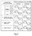
- Figure 2 shows the causes of partial discharge generated in metal enclosure 1 and the pattern of the resulting partial discharge pulse.
- Reason for partial discharge 1 may be further subdivided into case (1 - 1), in which discharge is produced due to the presence of bubbles or voids in the insulator in metal enclosure 1, and case (1 - 2), in which discharge is produced due to the formation of a gap at the contact surface of the insulator and conductor.
- Partial discharge 2 is produced when a part of the insulator projects into the region in metal enclosure 1 that is filled with insulating gas (sharp edge).
- Partial discharge 3 is produced when part of the metal projects into the region in metal enclosure 1 that is filled with insulating gas (loose metal particles).
- Partial discharge 4 is produced when there is poor contact at locations where one conductor is in contact with another conductor in metal enclosure 1.
- EP-A2-0-342 597 discloses an abnormality diagnosing system and method for high voltage power apparatus wherein a plurality of detectors for detecting abnormalities of the high voltage power apparatus and providing outputs indicative thereof are disposed to detect predetermined phenomena indicative of at least an insulation abnormality, power supply abnormality and foreign matter among abnormalities existing inside of the high voltage power apparatus
- a monitoring arrangement responsive to the outputs of the detectors provides at least one of an output and display of the kind of abnormality detected based on spectral analysis.
- WO92/06385 relevant under Article 54(3) EPC, discloses a diagnostic measuring system for gas insulated electrical substations having UHF couplers fitted to bus chambers monitors for partial discharge events within the chamber to identify the nature and location of an emergent breakdown condition.
- the system identifies each partial discharge event but characterises it by amplitude and its time of occurrence with respect to the start of the 50 Hz power frequency wave.
- the characterised events are communicated over an optical fibre link configured as a token passing ring to an analyzer where a comparison is made with stored historic data characterising known events.
- the analyser provides a self checking routine for the system.
- a microprocessor forming part of a unit associated with a plurality of couplers provides data compression of events identified from these couplers.
- a system for detecting partial discharge generated in the interior of gas-insulated switchgear comprises:
- the invention also extends to a method of detecting partial discharge generated in the interior of gas-insulated switchgear as defined in claim 8.
- Gas-insulated switchgear 12 is the same as that shown in Fig. 1.
- a voltage division circuit for the applied voltage is formed by floating capacitances C 1 and C 2 .
- the high-frequency component created by partial discharge occurring within metal enclosure 1 is superimposed on this divided voltage.
- High-frequency detecting device 22 of partial discharge detecting system 21 detects the high-frequency component contained in divided voltage V C2 between leads 5 and 6. It comprises a transformer 311 that transforms divided voltage V C2 , a band-pass filter 32 that extracts the high-frequency component caused by partial discharge in the output signal of transformer 311, and an amplifier 33 that amplifies the output signal of band-pass filter 32.
- a fundamental wave detecting device 23 which detects the fundamental wave component of divided voltage V C2 i.e., the mains frequency component. It comprises a transformer 312 that transforms divided voltage V C2 , a band-pass filter 39 that extracts the fundamental wave component of the output signal of transformer 312, and an amplifier 40 that amplifies the output signal of band-pass filter 39.
- the fundamental wave component of divided voltage V C2 extracted by fundamental wave detecting means 23 is input to a setting device 24 of the starting point for the voltage.
- Voltage starting point setting device 24 detects the zero-crossing point of the fundamental wave component of dividing voltage V C2 and outputs this as the starting point for the voltage, in the form of a pulse signal.
- This voltage starting point setting device 24 consists of a comparator 41 that detects the zero-crossing point of the output signal of fundamental wave detecting device 23 and outputs a pulse signal, and a pulse shaping circuit 42 that shapes the waveform of the pulse signal of comparator 41.
- the output signal of high-frequency detecting device 22 and the output signal of voltage starting point setting device 24 are input to a detected signal processing device 25.
- Detected signal processing device 25 carries out signal processing on the high-frequency component contained in dividing voltage V C2 detected by high-frequency detecting device 22 and on the pulse signal indicating the starting point for the voltage which is obtained by voltage starting point setting device 24 to produce a signal that is suitable for optical transmission to a partial discharge ascertaining device 26.
- the high-frequency component contained in divided voltage V C2 detected by high-frequency detecting device 22 is detected by a detector circuit 34 of detected signal processing device 25 and the output signal of detector circuit 34 is converted to a fixed pulse width by a peak hold circuit 35.
- the output signal of peak hold circuit 34 is then frequency-modulated by a V/F converter circuit. This frequency-modulated signal is then converted to an optical signal by an E/O converter 37 and input to partial discharge ascertaining device 26 through an optical fiber 281.
- the pulse signal from voltage starting point setting device 24 indicating the starting point for the voltage is input to a V/F converter 43 of detected signal processing device 25, where it is frequency-modulated.
- This frequency-modulated signal is then converted to an optical signal by an E/O converter 44, and input to partial discharge ascertaining device 26 through an optical fiber 282.
- Partial discharge ascertaining device 26 converts the optical signals that are input through optical fibers 281 and 282 into pulse signals P 3 and P 1 , respectively, (see Fig. 4). Based on pulse signal P 3 indicating the magnitude of the high-frequency component of dividing voltage V C2 and pulse signal P 1 indicating the starting point for the voltage of dividing voltage V C2 , partial discharge ascertaining device 26 ascertains whether partial discharge is taking place, and the reason or reasons for the occurrence of such partial discharge.
- the optical signal indicating the magnitude of the high-frequency component of the dividing voltage V C2 that is input from detected signal processing device 25 is converted to pulse signal P 3 indicating the magnitude of the high-frequency component of dividing voltage V C2 by means of an O/E converter 47, F/V converter 48, amplifier 49, and integrating circuit 50.
- the optical signal indicating the starting point for the voltage of dividing voltage V C2 that is input from detected signal processing device 25 is converted to pulse signal P 1 indicating the starting point for the voltage of dividing voltage V C2 by means of an O/E converter 53, F/V converter 54, amplifier 55, and waveform shaping circuit 56.
- Pulse signal P 1 indicating the starting point for the voltage is input to a computing element 29.
- Computing element 29 can be implemented using a CPU, a microprocessor or a computer, for example.
- computing element 29 Based on this pulse signal P 1 , computing element 29 outputs an instrumentation timing pulse signal P 2 to an A/D converter 51.
- A/D converter 51 introduces the pulse signal P 4 indicating the high frequency component into computing element 29 only during the period when instrumentation timing pulse signal P 2 is being input.
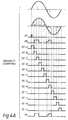
- Figs. 4A-4J are diagrams given in explanation of the operation of partial discharge detecting system partial discharge detecting system 21.
- fundamental wave component V 0 of dividing voltage V C2 contains a high frequency component V 1 .
- High frequency component V 1 contained in dividing voltage V C2 is detected by high-frequency detecting device 22 and the detected high frequency component V 1 is subjected to signal processing by detected signal processing device 25 to produce an optical signal which is optically transmitted to partial discharge ascertaining device 26.
- Fundamental wave component V 0 of dividing voltage V C2 is detected by fundamental wave detecting device 23.
- Voltage starting point setting device 24 then converts the zero-crossing point of fundamental wave component V 0 into a pulse signal constituting the starting point for the voltage. This is then subjected to signal processing by detected signal processing device 25 to produce an optical signal which is optically transmitted to partial discharge ascertaining device 26.
- Partial discharge ascertaining device 26 finds the high frequency component V 1 of dividing voltage V C2 as pulse signal P 3 and fundamental wave component V 0 of dividing voltage V C2 as pulse signal P 1 .
- Computing element 29 of detected signal processing means 25 outputs instrumentation timing pulse signal P 2 to A/D converter 51 based on pulse signal P 1 indicating the starting point for the voltage.
- Instrumentation timing pulse signal P 2 that is output by computing element 29 is a command signal, with reference to the starting point for the voltage, for introduction of pulse signal P 4 indicating the magnitude of the high-frequency component to computing element 29.
- signal P 4 is a digital signal to be input to computing element 29 in a form element 29 is able to process.
- the signal P 4 in Figs. 4A-4J is shown for convenience of explanation and does not represent the actual shape of the signal sent to element 29. The reason for partial discharge as indicated in Fig. 2 can therefore be determined.
- timing pulse signal P 2 which is a series of pulses P 2 -A to P 2 -L successively during the measurement time cycle period. While timing pulse signal P 2 is shown as consisting of twelve pulses P 2 -A to P 2 -L, it is understand that this is given by way of example only and the actual number of pulses can be varied based upon the requirements of the partial discharge detecting system and the gas-insulated switchgear.
- Fig. 4A corresponds to a partial discharge due to a vacancy or bubble corresponding to reason 1-1 in the starting discharge condition as shown in Fig. 2.
- the signals P 2-A to P 2-L are received by A/D converter 51 converts the partial discharge pulse P 3 to a digital signal which is input to computing element 29.
- Computing element 29 receives the digital signal P 4 from A/D converter 51 and stores signal P 4 in a memory section thereof. Computing element 29 then compares the stored signal P 4 with other patterns stored beforehand and determines whether a partial discharge has occurred based upon the signal P 4 . If it is determined that a partial discharge has occurred, that is, the signal P 4 corresponds to one of the known reasons for partial discharge, such as shown in Fig. 2, computing element 29 outputs a signal to an external display device and alarm 60 which displays the results of the partial discharge determination and produces an alarm. As is apparent from Fig. 4A, the signal P 4 provides both pulse magnitude and pulse phase information relative to the fundamental wave which allows the determination of whether a partial discharge has occurred.
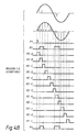
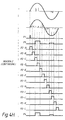
- FIGs. 4B-4J illustrate the determination of partial discharges corresponding to reasons 1-2, 2, 3 and 4 of the starting discharge condition and to reasons 1-1, 1-2, 2, 3 and 4 of the continuing discharge condition, respectively.
- computing element 29 is the same in each case, a detailed explanation of each Figure will be omitted for brevity.
- Fig. 5 is flow diagram given an explanation of the operation of the system shown in Fig.3.
- pulse signal P 1 is inputted to computing element 29, which triggers the output of timing pulse signal P 2 .
- step A which consists of steps 2A and 3A, pulse P 2 -A is outputted to A/D converter 51 and the portion of pulse signal P 4 occurring during the duration of pulse P 2 -A is inputted to computing element 29.
- steps B-L The same procedure as in step A is repeated in steps B-L such that all of the pulses of timing pulse signal P 2 are output to A/D converter 51 which converts pulse signal P 3 into digital signal P 4 , and the corresponding portions of digital signal P 4 are input to computing element 29.
- signal P 4 is stored in a memory section of computing element 29.
- Computing element 29 compares the stored digital signal P 4 with other stored known patterns which correspond to the partial discharge pattem shown in Fig. 2 (step 5). If the digital signal P 4 corresponds to one of the patterns, an alarm signal is generated and recorded in step 6. If the digital signal P 4 does not correspond to one of the partial discharge patterns, then the measurement cycle ends.
- the signal of specific frequency corresponding to partial discharge that is isolated by band-pass filter 32 often contains noise, which gives rise to measurement error. This noise cannot be removed by the conventional method of simply converting to a fixed pulse signal using a peak hold circuit or the like.
- pulse signals P 3 of specific frequency that are generated while instrumentation timing pulse signal P 2 is being output are subjected to A/D conversion and measured.
- Such a pulse of specified frequency is therefore present at a phase position, with respect to the phase of the main circuit voltage, at which partial discharge pulses are most likely to be generated, i.e., a phase position at which such a pulse is unlikely to be the result of noise.
- timing pulse P 2 can be output in the range where it is anticipated that partial discharge may occur.
- the cause of partial discharge can be ascertained from the pattern of occurrence by measuring whether there are any pulses of specified frequency in this range.
- a pulse resolution of about 1/100 of the period of the mains frequency is sufficient in order to measure partial discharge pulses in relation to the phase of the mains frequency voltage. Accordingly, in the system shown in Figure 3, the partial discharge pulses are subjected to peak-holding or integration within a time width on this order, forming pulse signals for optical transmission. These formed pulse signals are then V/F converted, then E/O converted, and transmitted optically to partial discharge ascertaining device 26 in a signal condition close to a digital signal. It is thereby possible to eliminate the effect of attenuation due to the length of the optical fiber cable or the effect of fluctuation in the amount of such attenuation due to the optical connector units. The time required for in situ adjustment of individual sensors can thereby be reduced, and unstable measurement conditions resulting from the amount of attenuation changing every time an optical connector is added or removed can be greatly reduced.
- Fig. 6 is a block diagram showing an embodiment of the invention. This embodiment represents an improvement over the system shown in Figure 3.
- errors can still be caused by external noise present having a frequency that is being measured entering gas-insulated switchgear 21 while instrumentation timing pulse signal P 2 is being output.
- the ingress of such external noise is infrequent and sporadic, it does present an obstacle to raising accuracy.
- the embodiment of the invention is adapted to eliminate causes of error due to such external noise.
- the frequency of partial discharge pulses occurring in gas-insulated switchgears is generally some tens of MHz.
- partial discharges caused by external noise entering the gas-insulated switchgear through parts such as the bushing of the gas-insulated switchgear are below some 100 KHz, sometimes overlaid with high-frequency components of some tens of MHz or more.
- high-frequency components below some 100 KHz cannot be detected within the gas-insulated switchgear, and can only be detected in the vicinity of the bushing.
- the gas-insulated switchgear can be regarded as a distributed-constant circuit. Such high-frequency components are therefore propagated through the switchgear with little attenuation. According to the invention, arrangements are made whereby, if external noise enters the gas-insulated switchgear and a partial discharge is generated due to high-frequency components of some tens of MHz superimposed on this external noise, this can be identified as not representing partial discharge originating from a cause to be found within the gas-insulated switchgear itself.
- Respective high-frequency detection devices 22A and 22B are provided that detect high-frequency components in two different locations within the same gas-insulated switchgear.
- FIG. 5 shows two gas-insulated switchgears 12A and 12B, it is understood that switchgears 12A and 12B are provided for convenience of explanation only, and that switchgears 12A and 12B are two portions of a single gas-insulated switchgear 12 having two bushing parts 12A and 12B.
- first high-frequency detection device 22A is provided on bushing part 12A of gas-insulated switchgear 12 having a detection frequency set to under some 100 kHz. This can be used to decide whether any external noise has entered.
- Second high-frequency detection device 22B positioned in the middle of gas-insulated switchgear 12 having a detection frequency set to over some tens of MHz. This can be used to decide whether partial discharge has occurred within gas-insulated switchgear 12.
- First detected signal processing device 25A that performs signal processing of the output signal of first high-frequency detection device 22A, fundamental wave detecting device 23, and voltage starting point setting device 24 are the same as in the system shown in Fig. 3.
- Second detected signal processing device 25B that performs signal processing of the output signal of second high-frequency detection device 22B is the same as first high-frequency detection device 25A except that it does not have units 43 and 44 that perform signal processing on the signal from voltage starting point setting device 24.
- partial discharge ascertaining device 26 is the same as that of Fig. 3 except that units 47B, 48B, 49B and 50B that perform signal processing on the signals obtained through second high-frequency detection device 22B and second detected signal processing device 25B are added to partial discharge ascertaining device 26 of Fig. 3.
- First high-frequency detection device 22A detects external noise that is generated at bushings in the same bus or overhead line.
- the detection frequency of second high-frequency detection device 22B is higher than that of first high-frequency detection device 22A, so, because of the difference in propagation characteristics described above, partial discharge pulses generated in the interior at central position 12B of gas-insulated switchgear 12 and high-frequency components superimposed on external noise are detected.
- pulse signal P 30 indicating the external noise and pulse signal P 31 indicating partial discharge
- pulse signal P 31 indicating partial discharge
- FIG. 7 there is shown a diagram similar to Fig. 4A given an explanation of the operation of the system of Fig. 3 but pulse signals of pulse timing signal P 2 have been omitted for brevity.
- Signal P 22A illustrates the fundamental wave having external noise detected by first high-frequency detecting device 22A.
- Units 47A, 48A, 49A, 50A, produce pulse signal P 30 which is input to A/D converter 51A. It is evident that signal P 30 provides both magnitude and phase information in relation to the fundamental wave of the noise detected by first high-frequency noise detecting device 22A.
- Second high-frequency detection device 22B connected to bushing part 12B detects the pulse signals on the fundamental wave which corresponds to signal P 22B .
- second detected signal processing device 25B and units 47B, 48B, 49B and 50B of partial discharge ascertaining device 26 produce signal P 31 which provides magnitude and phase information of the pulse signals detected by second high-frequency detection device 22B.
- Signal P 31 is input to A/D converter 51B in response to signal P 2 output from computing element 74.
- step 10 signal P 1 is inputted to computing device 74.
- computing element 74 Upon receiving signal P 1 , computing element 74 outputs pulse timing signal P 2 -A during step 20A of Step A.
- step 30A signals P 30 and P 31 are converted by A/O converters 51 A and 51 B, respectively, into digital signals P 40 and P 41 , which are inputted to computing element 74.
- pulse signals P 40 and P 41 which correspond to the digitized values of pulse signals P 30 and P 31 are input to computing element 74 in response to pulse signals P 2 -B to P 2 -L.
- Computing element 74 compares the input signals P 40 and P 41 and cancels the partial discharge pulses of signal P 41 which are detected at the same time as the noise pulses of signal P 40 to produce signal P 50 which is stored in computing elements 74 and compared to patterns in the same manner as the system of figure 3 (step 40). If the signal P 50 corresponds to one of the known discharge patterns (such as those shown in Fig. 2), the result is displayed and an alarm signal is generated using display device and alarm 60. On the other hand, if the signal P 50 does not correspond to one of the patterns, the measuring cycle ends.
- computing element 74 Based on pulse signal P 1 indicating the starting point for the voltage, computing element 74 outputs instrumentation timing pulse signal P 2 to A/D converters 51A and 51 B respectively.
- pulse signals P 40 and P 41 are input to computing element 74 practically simultaneously.
- signals P 40 , P 41 and P 50 are shown for convenience of explanation and do not represent the actual shape of the digital signal input to computing element 74. Any pulse signal P 41 which is input into computing element 74 is cancelled while pulse signal P 40 is also present at computing element 74.
Landscapes
- Physics & Mathematics (AREA)
- General Physics & Mathematics (AREA)
- Testing Relating To Insulation (AREA)
- Gas-Insulated Switchgears (AREA)
Claims (12)
- System zur Erfassung von Teilentladungen, die im Inneren eines gasisolierten Schalters entstehen, der bei einer Transformator-Anordnung verwendet wird, mit:einer ersten Hochfrequenzerfassungseinrichtung, die an einem Anschluß des gasisolierten Schalters vorgesehen ist, zum Erfassen einer ersten Hochfrequenzkomponente, die der an dem Leiter des gasisolierten Schalters anliegenden Spannung überlagert ist und durch in den gasisolierten Schalter eintretendes Fremdrauschen verursacht wird;einer zweiten Hochfrequenzerfassungseinrichtung, die an einer mittleren Stelle des gasisolierten Schalters vorgesehen ist, zum Erfassen einer zweiten Hochfrequenzkomponente, die der an dem Leiter des gasisolierten Schalters anliegenden Spannung überlagert ist und durch Teilentladungen im Inneren des gasisolierten Schalters verursacht wird;einer Grundwellenerfassungseinrichtung zum Erfassen einer Grundwellenkomponente von der an dem Leiter des gasisolierten Schalters anliegenden Spannung;einer Spannungsstartpunkteinstelleinrichtung zum Erfassen eines Nulldurchgangspunktes der Grundwellenkomponente, die von der Grundwellenerfassungseinrichtung erhalten wird, und zum Einstellen eines Startpunktes, der auf dem Nulldurchgangspunkt basiert;einer Einrichtung zur Verarbeitung erfaßter Signale zum Durchführen einer Signalverarbeitung eines ersten Ausgangssignals der ersten Hochfrequenzerfassungseinrichtung, eines zweiten Ausgangssignals der zweiten Hochfrequenzerfassungseinrichtung und eines dritten Ausgangssignals der Spannungsstartpunkteinstelleinrichtung, und zum Ausgeben von ersten, zweiten bzw. dritten optischen Signalen, die den ersten, zweiten und dritten Ausgangssignalen entsprechen; undeiner Teilentladungsentscheidungseinrichtung zum Umwandeln der ersten, zweiten und dritten optischen Signale von der Einrichtung zur Verarbeitung erfaßter Signale in zugehörige erste, zweite und dritte Impulssignale und zum Feststellen eines Auftretens von Teilentladungen und einer Ursache für das Auftreten von Teilentladungen, basierend auf den ersten und zweiten Impulssignalen und auf der Phasenbeziehung zwischen den ersten, zweiten und dritten Impulssignalen.
- System nach Anspruch 1, bei dem die Teilentladungsentscheidungseinrichtung aufweist:eine erste Umwandlungseinrichtung zum Umwandeln des ersten Impulssignals in ein erstes digitales Signal;eine zweite Umwandlungseinrichtung zum Umwandeln des zweiten Impulssignals in ein zweites digitales Signal; undeine Berechnungseinrichtung zum Ausgeben eines Zeitimpulssignals bei Empfang des dritten Impulssignals an die erste und zweite Umwandlungseinrichtung, die bei Empfang des Zeitimpulssignals jeweils die ersten und zweiten digitalen Signale an die Berechnungseinrichtung ausgeben, zum Entfernen von Teilen des zweiten digitalen Signals, die im wesentlichen gleichzeitig mit dem ersten digitalen Signal in die Berechnungseinrichtung eingehen, und zum Speichern verbleibender Teile des zweiten digitalen Signals, um die gespeicherten Teile des zweiten digitalen Signals mit bekannten Referenzmustern zu vergleichen, die Mustern von Teilentladungen entsprechen, und zum Ausgeben eines Signals, das das Auftreten von Teilentladungen angibt, und einer Ursache für das Auftreten von Teilentladungen, wenn die gespeicherten Teile des zweiten digitalen Signals zumindest einem der bekannten Referenzmuster entsprechen.
- System nach Anspruch 2, bei dem die Berechnungseinrichtung außerdem eine Speichereinrichtung zum Speichern der Teile des zweiten digitalen Signals und der bekannten Muster von Teilentladungen aufweist.
- System nach Anspruch 2, bei dem die Berechnungseinrichtung eine Einrichtung zum Erzeugen des Zeitimpulssignals als eine Reihe von aufeinanderfolgenden Impulssignalen über einen einzelnen Zyklus der Grundwellenkomponente aufweist.
- System nach Anspruch 1, bei dem die erste Hochfrequenzerfassungseinrichtung aufweist:einen ersten Bandpaßfilter zum Herausfiltern der ersten Hochfrequenzkomponente der Spannung und zum Ausgeben eines ersten Signals; undeinen ersten Verstärker zum Verstärken des ersten Signals;wobei die zweite Hochfrequenzerfassungseinrichtung aufweist:einen zweiten Bandpaßfilter zum Herausfiltern der zweiten Hochfrequenzkomponente der Spannung und zum Ausgeben eines zweiten Signals; undeinen zweiten Verstärker zum Verstärken des zweiten Signals;wobei die Grundwellenerfassungseinrichtung aufweist:einen dritten Bandpaßfilter zum Herausfiltern der Grundwellenkomponente und zum Ausgeben eines dritten Signals; undeinen dritten Verstärker zum Verstärken des dritten Signals;wobei die Spannungsstartpunkteinstelleinrichtung aufweist:einen Vergleicher zum Erfassen des Nulldurchgangspunktes der Grundwellenkomponente unter Verwendung des verstärkten dritten Signals und zum Ausgeben eines vierten Signals; undeine Impulsformungseinrichtung zur Impulsformung des vierten Signals und zum Ausgeben eines fünften Signals; undwobei die Einrichtung zur Verarbeitung erfaßter Signale aufweist:eine erste Erfassungseinrichtung zum Erfassen der ersten Hochfrequenzkomponente unter Verwendung des verstärkten ersten Signals und zum Ausgeben eines sechsten Signals;eine erste Spitzenwerthalteeinrichtung zum Umwandeln des sechsten Signals in ein erstes Signal mit fester Impulsbreite;eine erste Frequenzmodulationseinrichtung zur Frequenzmodulation des ersten Signals mit fester Impulsbreite; undeine erste optische Umwandlungseinrichtung zum Umwandeln des frequenzmodulierten ersten Signals mit fester Impulsbreite in das erste optische Signal;eine zweite Erfassungseinrichtung zum Erfassen der zweiten Hochfrequenzkomponente unter Verwendung des verstärkten ersten Signals und zum Ausgeben eines siebten Signals;eine zweite Spitzenwerthalteeinrichtung zum Umwandeln des siebten Signals in ein zweites Signal mit fester Impulsbreite;eine zweite Frequenzmodulationseinrichtung zur Frequenzmodulation des zweiten Signals mit fester Impulsbreite;eine zweite optische Umwandlungseinrichtung zum Umwandeln des frequenzmodulierten zweiten Signals mit fester Impulsbreite in das zweite optische Signal;eine dritte Frequenzmodulationseinrichtung zur Frequenzmodulation des fünften Signals; undeine dritte optische Umwandlungseinrichtung zum Umwandeln des frequenzmodulierten fünften Signals in das dritte optische Signal.
- System nach Anspruch 5, bei dem:der erste Bandpaßfilter eine erste Bandpaßfilterfrequenz hat; undder zweite Bandpaßfilter eine zweite Bandpaßfilterfrequenz hat, die kleiner ist als die erste Bandpaßfilterfrequenz.
- System nach Anspruch 1, bei dem die Teilentladungsentscheidungseinrichtung aufweist:eine erste optische Umwandlungseinrichtung zum Umwandeln des ersten optischen Signals in ein erstes frequenzmoduliertes Signal;eine erste Frequenzumwandlungseinrichtung zum Umwandeln des ersten frequenzmodulierten Signals in ein erstes Spannungssignal;einen ersten Verstärker zum Verstärken des ersten Spannungssignals;eine erste Integriereinrichtung zum Integrieren des verstärkten ersten Spannungssignals und zum Ausgeben des ersten Impulssignals;eine zweite optische Umwandlungseinrichtung zum Umwandeln des zweiten optischen Signals in ein zweites frequenzmoduliertes Signal;eine zweite Frequenzumwandlungseinrichtung zum Umwandeln des zweiten frequenzmodulierten Signals in ein zweites Spannungssignal;einen zweiten Verstärker zum Verstärken des zweiten Spannungssignals;eine zweite Integriereinrichtung zum Integrieren des verstärkten zweiten Spannungssignals und zum Ausgeben des zweiten Impulssignals;eine dritte optische Umwandlungseinrichtung zum Umwandeln des dritten optischen Signals in ein drittes frequenzmoduliertes Signal;eine dritte Frequenzumwandlungseinrichtung zum Umwandeln des dritten frequenzmodulierten Signals in ein drittes Spannungssignal;einen dritten Verstärker zum Verstärken des dritten Spannungssignals;eine Signalformformungseinrichtung zum Erzeugen des dritten Impulssignals unter Verwendung des verstärkten dritten Spannungssignals; undeine Berechnungseinrichtung zum Ausgeben eines Impulszeitsignals bei Empfang des dritten Impulssignals von der Signalformformungseinrichtung an die erste und zweite Umwandlungseinrichtung, die jeweils die ersten und zweiten digitalen Signale an die Berechnungseinrichtung ausgeben, und zum Bestimmen des Auftretens von Teilentladungen und der Ursache für das Auftreten unter Verwendung der digitalen Signale.
- Verfahren zur Erfassung von Teilentladungen, die im Inneren eines gasisolierten Schalters entstehen, mit den folgenden Schritten:Erfassen einer ersten Hochfrequenzkomponente von einer an einem Leiter des gasisolierten Schalters anliegenden Spannung, die durch längeres Rauschen verursacht wird, das die Spannung überlagert;Erfassen einer zweiten Hochfrequenzkomponente von der an dem Leiter des gasisolierten Schalters anliegenden Spannung, die durch Teilentladungen im Inneren des gasisolierten Schalters verursacht wird;Erfassen einer Grundwellenkomponente von der an dem Leiter des gasisolierten Schalters anliegenden Spannung;Erfassen eines Nulldurchgangspunktes der Grundwellenkomponente und Einstellen eines dritten Signals, das ein Startpunktsignal enthält, das auf dem Nulldurchgangspunkt basiert;Durchführen einer Signalverarbeitung bei der ersten Hochfrequenzkomponente, der zweiten Hochfrequenzkomponente und dem dritten Signal und Erzeugen von entsprechenden ersten, zweiten und dritten optischen Signalen;Umwandeln der ersten, zweiten und dritten optischen Signale in jeweilige erste, zweite und dritte Impulssignale und Feststellen des Auftretens von Teilentladungen und einer Ursache für das Auftreten von Teilentladungen, basierend auf den ersten und zweiten Impulssignalen und auf der Phasenbeziehung zwischen den ersten, zweiten und dritten Impulssignalen.
- Verfahren nach Anspruch 8, bei dem der Schritt des Feststellens umfaßt:Bestimmen eines ersten Musters der ersten Hochfrequenzkomponente anhand einer Phasenbeziehung mit der Grundwellenkomponente unter Verwendung des Startpunktes;Bestimmen eines zweiten Musters der zweiten Hochfrequenzkomponente anhand der Phasenbeziehung mit der Grundwellenkomponente unter Verwendung des Startpunktes;Bestimmen eines dritten Musters durch Entfernen von Teilen des zweiten Musters, die sich mit dem ersten Muster überlappen;Vergleichen des dritten Musters mit bekannten Mustern der Teilentladungen; undBestimmen, ob Teilentladungen stattgefunden haben, und der Ursache für das Auftreten der Teilentladungen, wenn das dritte Muster zumindest einem der bekannten Muster entspricht.
- Verfahren nach Anspruch 8, das außerdem umfaßt:Erfassen jeweiliger Werte der ersten und zweiten Hochfrequenzkomponenten und jeweiliger Phasenbeziehungen der ersten und zweiten Hochfrequenzkomponentes bezüglich des Startpunkts der Spannung;Feststellen von ersten bzw. zweiten Mustern der ersten und zweiten Hochfrequenzkomponenten unter Verwendung sowohl der jeweiligen Werte der ersten und zweiten Hochfrequenzkomponenten als auch der jeweiligen Phasenbeziehungen der ersten und zweiten Hochfrequenzkomponenten bezüglich des Startpunkts der Spannung;Erzeugen eines dritten Musters durch Entfernen von Teilen des zweiten Musters, die sich mit dem ersten Muster überlappen;Vergleichen des dritten Musters mit bekannten Mustern der Teilentladungen; undFeststellen, ob Teilentladungen stattgefunden haben, und der Ursache für das Auftreten der Teilentladungen, wenn das dritte Muster zumindest einem der bekannten Muster entspricht.
- Verfahren nach Anspruch 8, bei dem der Feststellungsschritt umfaßt:Feststellen eines Vorhandenseins der ersten und zweiten Hochfrequenzkomponenten für eine vorbestimmte Anzahl von Perioden während eines Zyklus von der Grundwellenkomponente;Erzeugen von ersten bzw. zweiten Mustern, die jeweils das Vorhandensein von ersten und zweiten Hochfrequenzkomponenten während der Perioden darstellen;Erzeugen eines dritten Musters durch Entfernen von Teilen des zweiten Musters, die sich mit dem ersten Muster überlappen;Vergleichen des dritten Musters mit bekannten Mustern der Teilentladungen; undBestimmen, ob Teilentladungen stattgefunden haben, und der Ursache für das Auftreten dieser Teilentladungen, wenn das dritte Muster zumindest einem der bekannten Muster entspricht.
- Verfahren nach Anspruch 8, das außerdem umfaßt:Frequenzmodulieren der erfaßten ersten und zweiten Hochfrequenzkomponenten und der Grundwellenkomponente;Umwandeln der frequenzmodulierten ersten und zweiten Hochfrequenzkomponenten und der frequenzmodulierten Grundwellenkomponente in die ersten, zweiten bzw. dritten optischen Signale;Ausgeben der ersten, zweiten und dritten optischen Signale in ein Glasfasernetzwerk;Empfangen der ersten, zweiten und dritten optischen Signale aus dem Glasfasernetzwerk und Umwandeln der ersten, zweiten und dritten optischen Signale in erste, zweite und dritte frequenzmodulierte Signale;Umwandeln der ersten, zweiten und dritten frequenzmodulierten Signale in die ersten, zweiten und dritten Impulssignale;Ausgeben des dritten Impulssignals an eine Berechnungseinrichtung;Umwandeln der ersten und zweiten Impulssignale in erste bzw. zweite digitale Signale; undEingeben der ersten und zweiten digitalen Signale in die Berechnungseinrichtung in Reaktion auf das Empfangen des dritten Impulssignals durch die Berechnungseinrichtung;Erzeugen eines dritten digitalen Signals durch Entfernen von Teilen des zweiten digitalen Signals, die sich mit dem ersten digitalen Signal überlappen, Vergleichen des dritten digitalen Signals mit digitalen Signalen, die bekannte Muster der Teilentladungen darstellen, und Erfassen, ob Teilentladungen stattgefunden haben, und der Ursache für das Stattfinden dieser Teilentladungen, wenn das dritte digitale Signal zumindest einem der digitalen Signale entspricht, die die bekannten Muster der Teilentladungen darstellen, unter Verwendung der Berechnungseinrichtung.
Applications Claiming Priority (3)
| Application Number | Priority Date | Filing Date | Title |
|---|---|---|---|
| JP336733/90 | 1990-11-30 | ||
| JP33673390 | 1990-11-30 | ||
| JP2336733A JPH04204270A (ja) | 1990-11-30 | 1990-11-30 | ガス絶縁開閉装置の部分放電検出装置 |
Publications (4)
| Publication Number | Publication Date |
|---|---|
| EP0488719A2 EP0488719A2 (de) | 1992-06-03 |
| EP0488719A3 EP0488719A3 (en) | 1992-11-04 |
| EP0488719B1 EP0488719B1 (de) | 1998-01-14 |
| EP0488719B2 true EP0488719B2 (de) | 2001-04-18 |
Family
ID=18302217
Family Applications (1)
| Application Number | Title | Priority Date | Filing Date |
|---|---|---|---|
| EP91310997A Expired - Lifetime EP0488719B2 (de) | 1990-11-30 | 1991-11-28 | System und Methode zur Detektion von Teilentladungen von gasisolierten Schaltern |
Country Status (5)
| Country | Link |
|---|---|
| US (1) | US5200737A (de) |
| EP (1) | EP0488719B2 (de) |
| JP (1) | JPH04204270A (de) |
| KR (1) | KR960004555B1 (de) |
| DE (1) | DE69128698T3 (de) |
Families Citing this family (42)
| Publication number | Priority date | Publication date | Assignee | Title |
|---|---|---|---|---|
| EP0491554B1 (de) * | 1990-12-17 | 1996-05-22 | Patented Devices (Proprietary) Limited | Überwachung von Teilentladungen |
| US5256977A (en) * | 1991-11-22 | 1993-10-26 | Axis Usa, Inc. | High frequency surge tester methods and apparatus |
| GB2270217B (en) * | 1992-08-27 | 1996-04-10 | Univ Bath | Detecing faults in power lines |
| JP2952737B2 (ja) * | 1993-03-24 | 1999-09-27 | 日新電機株式会社 | 電力機器の部分放電検出装置 |
| FR2721408B1 (fr) * | 1994-06-20 | 1996-08-02 | Schneider Electric Sa | Dispositif de détection de décharges électriques pour appareillage électrique. |
| US5590012A (en) * | 1995-03-30 | 1996-12-31 | Siemens Energy & Automation, Inc. | Electric arc detector sensor circuit |
| DE19531827B4 (de) * | 1995-08-15 | 2005-05-04 | Siemens Ag | Meßsystem für elektrische Störungen in einer Hochspannungsschaltanlage |
| DE29518286U1 (de) * | 1995-11-17 | 1996-01-18 | Siemens AG, 80333 München | Vorrichtung zur Ortung von Teilentladungen bei dynamoelektrischen Hochspannungsmaschinen und/oder Hochspannungsanlagen |
| WO1997028588A1 (de) * | 1996-01-31 | 1997-08-07 | Siemens Aktiengesellschaft | Metallgekapselte schaltanlage mit teilentladungserfassung |
| DE19626527A1 (de) * | 1996-07-02 | 1998-01-08 | Abb Research Ltd | Verfahren zur Erfassung von Teilentladungsimpulsen und Einrichtung zur Durchführung des Verfahrens |
| JPH10170596A (ja) * | 1996-12-09 | 1998-06-26 | Hitachi Ltd | 絶縁機器診断システム及び部分放電検出法 |
| NL1005721C2 (nl) * | 1997-04-03 | 1998-10-07 | Kema Nv | Werkwijze en inrichting voor het detecteren van partiële ontladingen. |
| DE19734552C2 (de) * | 1997-07-31 | 2003-01-30 | Siemens Ag | Vorrichtung und Verfahren zur Messung von Teilentladungen in gasisolierten Hochspannungsanlagen |
| DE19749986A1 (de) * | 1997-11-12 | 1999-05-27 | Abb Patent Gmbh | Hochspannungsschaltanlage |
| US6313640B1 (en) * | 1998-02-03 | 2001-11-06 | Abb Power T & D Company, Inc. | System and method for diagnosing and measuring partial discharge |
| US6414829B1 (en) * | 1998-02-19 | 2002-07-02 | Square D Company | Arc fault circuit interrupter |
| FR2783348B1 (fr) | 1998-09-15 | 2000-10-13 | Alstom Technology | Methode de discrimination entre un arc interne et un arc de coupure dans un disjoncteur de moyenne ou de haute tension |
| US6242922B1 (en) * | 1998-11-06 | 2001-06-05 | General Electric Company | Arc detection architecture based on correlation for circuit breakers |
| JP4157636B2 (ja) | 1999-01-28 | 2008-10-01 | 株式会社日立製作所 | ガス絶縁機器の部分放電診断装置 |
| KR100477215B1 (ko) * | 2002-04-10 | 2005-03-21 | 학교법인 성균관대학 | 웨이브렛변환을 이용한 가스절연개폐장치의 부분방전검출방법 |
| GB0306282D0 (en) * | 2003-03-19 | 2003-04-23 | Diagnostic Monitoring Systems | Improved system for monitoring electrical components |
| JP4470157B2 (ja) | 2004-02-20 | 2010-06-02 | 株式会社日本Aeパワーシステムズ | 部分放電測定方法及びその装置 |
| JP4323418B2 (ja) * | 2004-12-16 | 2009-09-02 | 株式会社日本Aeパワーシステムズ | ガス絶縁機器の異常状態診断方法およびシステム |
| JP5078276B2 (ja) * | 2006-04-21 | 2012-11-21 | 三菱電機株式会社 | 診断用信号処理装置 |
| ITPR20060054A1 (it) * | 2006-06-13 | 2007-12-14 | Techimp S R L | Strumento e procedimento di rilevazione di scariche elettriche parziali in un sistema elettrico |
| TWI308640B (en) * | 2006-12-27 | 2009-04-11 | Ind Tech Res Inst | Portable partial discharge detection device and method thereof |
| KR100968519B1 (ko) * | 2008-07-14 | 2010-07-08 | (주) 피에스디테크 | 전력설비의 부분방전 노이즈 제거 장치 및 부분방전발생구간 검출 장치 |
| UA104429C2 (uk) * | 2008-08-06 | 2014-02-10 | Еском Холдінгс Лімітед | Спосіб і система моніторингу часткових розрядів |
| US8098072B2 (en) * | 2008-09-24 | 2012-01-17 | Siemens Energy, Inc. | Partial discharge coupler for application on high voltage generator bus works |
| KR20090075657A (ko) * | 2009-06-19 | 2009-07-08 | 한빛이디에스(주) | 가스절연 개폐장치 진단용 부분방전 카운터 |
| EP2290385A1 (de) * | 2009-08-25 | 2011-03-02 | ABB Technology AG | Überwachungssystem für Leistungstransformatoren und Überwachungsverfahren |
| US9612271B2 (en) * | 2010-03-05 | 2017-04-04 | Ericsson Inc. | Evaluating noise and excess current on a power line |
| CN202502197U (zh) * | 2012-03-20 | 2012-10-24 | 上海市电力公司 | 一种用于电容器局部放电在线监测系统的放大装置 |
| CN109154786B (zh) * | 2016-05-17 | 2020-12-04 | Asml荷兰有限公司 | 基于贯穿波长的相似性的度量强健性 |
| KR101787901B1 (ko) * | 2016-06-14 | 2017-11-15 | 엘에스산전 주식회사 | 전력설비 진단장치 |
| JP6986859B2 (ja) * | 2017-05-22 | 2021-12-22 | 三菱電機株式会社 | 部分放電検出装置及び部分放電検出装置の設置方法 |
| CA3007729A1 (en) | 2017-06-12 | 2018-12-12 | Vibrosystm Inc. | Method of monitoring partial discharges in a high voltage electric machine, and connection cable therefore |
| KR102189498B1 (ko) * | 2019-03-05 | 2020-12-11 | 엘에스일렉트릭(주) | 배전반내 부분방전 모니터링 시스템 및 장치 |
| GB2588133A (en) * | 2019-10-08 | 2021-04-21 | Ea Tech Limited | Partial discharge monitoring device, system and method for a substation asset provided with a voltage presence indication system (VPIS) |
| CN111679181A (zh) * | 2020-06-19 | 2020-09-18 | 国网陕西省电力公司电力科学研究院 | 一种高压无功投切开关触头烧蚀的带电检测方法及装置 |
| JP7851979B2 (ja) * | 2024-03-26 | 2026-04-27 | 株式会社東芝 | 部分放電診断装置、部分放電診断方法、及び部分放電診断システム |
| CN118425707B (zh) * | 2024-07-01 | 2024-09-24 | 国网浙江省电力有限公司电力科学研究院 | 局部放电检测的自适应去噪方法、系统、设备及介质 |
Family Cites Families (14)
| Publication number | Priority date | Publication date | Assignee | Title |
|---|---|---|---|---|
| US3775676A (en) * | 1972-07-21 | 1973-11-27 | Westinghouse Electric Corp | Methods for locating partial discharges in electrical apparatus |
| US3801899A (en) * | 1973-03-26 | 1974-04-02 | Gen Electric | Means for detecting the inception of corona discharges within induction apparatus |
| US4095173A (en) * | 1976-12-27 | 1978-06-13 | General Electric Company | Method and system for corona source location by acoustic signal detection |
| JPS6016163B2 (ja) * | 1978-02-03 | 1985-04-24 | 株式会社日立製作所 | ガス絶縁電気機器およびその部分放電検出方法 |
| US4245187A (en) * | 1979-05-10 | 1981-01-13 | The United States Of America As Represented By The Secretary Of The Navy | VLF Capacitor corona detection |
| US4238733A (en) * | 1979-05-15 | 1980-12-09 | Canadian General Electric Company Limited | Corona discharge monitor system |
| US4466071A (en) * | 1981-09-28 | 1984-08-14 | Texas A&M University System | High impedance fault detection apparatus and method |
| US4547769A (en) * | 1981-10-30 | 1985-10-15 | Kabushiki Kaisha Meidensha | Vacuum monitor device and method for vacuum interrupter |
| US4446420A (en) * | 1982-01-28 | 1984-05-01 | Hydro Quebec | Method and device for detecting and locating fault and/or partial discharges in a gas-insulated electrical equipment |
| DE3347185A1 (de) * | 1983-12-27 | 1985-07-04 | Siemens AG, 1000 Berlin und 8000 München | Anordnung zur beeinflussung eines schaltgeraetes |
| JPS6415670A (en) * | 1987-07-09 | 1989-01-19 | Toshiba Corp | Internal partial discharge detection system of gas insulated switch apparatus |
| JPH0738011B2 (ja) * | 1988-05-16 | 1995-04-26 | 株式会社日立製作所 | 高圧電力機器の異常診断システム |
| JP2774645B2 (ja) * | 1990-02-28 | 1998-07-09 | 株式会社東芝 | 部分放電検出器 |
| GB9021484D0 (en) * | 1990-10-03 | 1990-11-14 | Univ Strathclyde | Gas insulated substations |
-
1990
- 1990-11-30 JP JP2336733A patent/JPH04204270A/ja active Pending
-
1991
- 1991-11-28 KR KR1019910021498A patent/KR960004555B1/ko not_active Expired - Fee Related
- 1991-11-28 EP EP91310997A patent/EP0488719B2/de not_active Expired - Lifetime
- 1991-11-28 DE DE69128698T patent/DE69128698T3/de not_active Expired - Fee Related
- 1991-11-29 US US07/799,945 patent/US5200737A/en not_active Expired - Fee Related
Non-Patent Citations (4)
| Title |
|---|
| Bodden M.: Binaurale Signalverarbeitung: Modellierung der Richtungserkennung und des Coktail-Party-Effektes, Fortschritt Berichte, VDI, Reihe 17, Nr.85, VDI Verlag, 1992. † |
| Gaik W.: Untersuchungen zur binauralen Verarbeitung kopfbezogener Signale, Fortschritt Berichte,VDI,Reihe 17, Nr.63, VDI Verlag, 1990. † |
| Krump: Ein störsignalresistentes Verfahren zur computergestützten Teilentladungsdiagnostik in SF6-isolierten Schaltanlagen, PhD-thesis at the Bergische Universität-Gesamthochschule Wuppertal, published not laten than 24/02/90. † |
| Peissig J.: <binaurale Hörgerätestrategien in komplexe Störschallsituationen Dissertation Universität Göttingen , 1992. † |
Also Published As
| Publication number | Publication date |
|---|---|
| EP0488719A3 (en) | 1992-11-04 |
| JPH04204270A (ja) | 1992-07-24 |
| US5200737A (en) | 1993-04-06 |
| DE69128698D1 (de) | 1998-02-19 |
| DE69128698T3 (de) | 2001-08-16 |
| EP0488719B1 (de) | 1998-01-14 |
| KR920010692A (ko) | 1992-06-27 |
| DE69128698T2 (de) | 1998-06-04 |
| EP0488719A2 (de) | 1992-06-03 |
| KR960004555B1 (ko) | 1996-04-09 |
Similar Documents
| Publication | Publication Date | Title |
|---|---|---|
| EP0488719B2 (de) | System und Methode zur Detektion von Teilentladungen von gasisolierten Schaltern | |
| KR100691655B1 (ko) | 가스절연기기의 부분방전진단장치 및 진단방법 | |
| KR200278981Y1 (ko) | 방사 전자파를 이용한 전력기기의 부분방전 검출장치 | |
| US4245187A (en) | VLF Capacitor corona detection | |
| US6424162B1 (en) | Insulated device diagnosing system that prepares detection data from partial discharge signal such that periodic elements are given to different specific frequencies of the partial discharge signal | |
| KR0153253B1 (ko) | 가스절연 전기 기기의 이상위치 기록장치 및 방법 | |
| US4975800A (en) | Contact abnormality detecting system | |
| US5396180A (en) | System for monitoring gas insulated substations | |
| JP3352278B2 (ja) | 部分放電検出方法 | |
| KR100577347B1 (ko) | 가스절연 개폐장치용 단로기의 진단장치 및 진단방법 | |
| KR100360018B1 (ko) | 전력기기의 부분방전 검출장치 | |
| JP2774645B2 (ja) | 部分放電検出器 | |
| JPH0980111A (ja) | 部分放電検出装置 | |
| JP2001133503A (ja) | ノイズ検知方法及びこれを用いたメンテナンスシステム | |
| JPS6219774A (ja) | 高電圧機器の部分放電検出装置 | |
| JPH0712880A (ja) | 部分放電検出法 | |
| JP3126392B2 (ja) | ガス絶縁開閉装置の部分放電検出装置 | |
| KR100632078B1 (ko) | 초고압 케이블의 부분방전 측정 시 노이즈 제거장치 및방법 | |
| JP3126391B2 (ja) | 部分放電検出器 | |
| CN116027150A (zh) | 检测中压电气设备的电导体中的异常事件的方法 | |
| JPH04215076A (ja) | 部分放電測定方法 | |
| JP2774649B2 (ja) | 部分放電検出器 | |
| JP2723902B2 (ja) | スペクトラム減算方式部分放電監視システム | |
| JP3195862B2 (ja) | 部分放電検出装置 | |
| JPH0574256A (ja) | 部分放電測定装置 |
Legal Events
| Date | Code | Title | Description |
|---|---|---|---|
| PUAI | Public reference made under article 153(3) epc to a published international application that has entered the european phase |
Free format text: ORIGINAL CODE: 0009012 |
|
| 17P | Request for examination filed |
Effective date: 19911213 |
|
| AK | Designated contracting states |
Kind code of ref document: A2 Designated state(s): CH DE FR GB LI SE |
|
| PUAL | Search report despatched |
Free format text: ORIGINAL CODE: 0009013 |
|
| AK | Designated contracting states |
Kind code of ref document: A3 Designated state(s): CH DE FR GB LI SE |
|
| 17Q | First examination report despatched |
Effective date: 19950712 |
|
| GRAG | Despatch of communication of intention to grant |
Free format text: ORIGINAL CODE: EPIDOS AGRA |
|
| GRAG | Despatch of communication of intention to grant |
Free format text: ORIGINAL CODE: EPIDOS AGRA |
|
| GRAH | Despatch of communication of intention to grant a patent |
Free format text: ORIGINAL CODE: EPIDOS IGRA |
|
| GRAH | Despatch of communication of intention to grant a patent |
Free format text: ORIGINAL CODE: EPIDOS IGRA |
|
| GRAA | (expected) grant |
Free format text: ORIGINAL CODE: 0009210 |
|
| AK | Designated contracting states |
Kind code of ref document: B1 Designated state(s): CH DE FR GB LI SE |
|
| REG | Reference to a national code |
Ref country code: CH Ref legal event code: NV Representative=s name: WILLIAM BLANC & CIE CONSEILS EN PROPRIETE INDUSTRI Ref country code: CH Ref legal event code: EP |
|
| ET | Fr: translation filed | ||
| REF | Corresponds to: |
Ref document number: 69128698 Country of ref document: DE Date of ref document: 19980219 |
|
| PLBI | Opposition filed |
Free format text: ORIGINAL CODE: 0009260 |
|
| PLBF | Reply of patent proprietor to notice(s) of opposition |
Free format text: ORIGINAL CODE: EPIDOS OBSO |
|
| 26 | Opposition filed |
Opponent name: SIEMENS AG Effective date: 19981005 |
|
| PLBF | Reply of patent proprietor to notice(s) of opposition |
Free format text: ORIGINAL CODE: EPIDOS OBSO |
|
| PLBF | Reply of patent proprietor to notice(s) of opposition |
Free format text: ORIGINAL CODE: EPIDOS OBSO |
|
| PLAW | Interlocutory decision in opposition |
Free format text: ORIGINAL CODE: EPIDOS IDOP |
|
| PLAW | Interlocutory decision in opposition |
Free format text: ORIGINAL CODE: EPIDOS IDOP |
|
| PUAH | Patent maintained in amended form |
Free format text: ORIGINAL CODE: 0009272 |
|
| STAA | Information on the status of an ep patent application or granted ep patent |
Free format text: STATUS: PATENT MAINTAINED AS AMENDED |
|
| 27A | Patent maintained in amended form |
Effective date: 20010418 |
|
| AK | Designated contracting states |
Kind code of ref document: B2 Designated state(s): CH DE FR GB LI SE |
|
| REG | Reference to a national code |
Ref country code: CH Ref legal event code: AEN Free format text: MAINTIEN DU BREVET DONT L'ETENDUE A ETE MODIFIEE |
|
| ET3 | Fr: translation filed ** decision concerning opposition | ||
| REG | Reference to a national code |
Ref country code: GB Ref legal event code: IF02 |
|
| PGFP | Annual fee paid to national office [announced via postgrant information from national office to epo] |
Ref country code: SE Payment date: 20031105 Year of fee payment: 13 |
|
| PGFP | Annual fee paid to national office [announced via postgrant information from national office to epo] |
Ref country code: FR Payment date: 20031110 Year of fee payment: 13 |
|
| PGFP | Annual fee paid to national office [announced via postgrant information from national office to epo] |
Ref country code: GB Payment date: 20031126 Year of fee payment: 13 |
|
| PGFP | Annual fee paid to national office [announced via postgrant information from national office to epo] |
Ref country code: CH Payment date: 20031128 Year of fee payment: 13 |
|
| PGFP | Annual fee paid to national office [announced via postgrant information from national office to epo] |
Ref country code: DE Payment date: 20031211 Year of fee payment: 13 |
|
| PG25 | Lapsed in a contracting state [announced via postgrant information from national office to epo] |
Ref country code: GB Free format text: LAPSE BECAUSE OF NON-PAYMENT OF DUE FEES Effective date: 20041128 |
|
| PG25 | Lapsed in a contracting state [announced via postgrant information from national office to epo] |
Ref country code: SE Free format text: LAPSE BECAUSE OF NON-PAYMENT OF DUE FEES Effective date: 20041129 |
|
| PG25 | Lapsed in a contracting state [announced via postgrant information from national office to epo] |
Ref country code: LI Free format text: LAPSE BECAUSE OF NON-PAYMENT OF DUE FEES Effective date: 20041130 Ref country code: CH Free format text: LAPSE BECAUSE OF NON-PAYMENT OF DUE FEES Effective date: 20041130 |
|
| PG25 | Lapsed in a contracting state [announced via postgrant information from national office to epo] |
Ref country code: DE Free format text: LAPSE BECAUSE OF NON-PAYMENT OF DUE FEES Effective date: 20050601 |
|
| EUG | Se: european patent has lapsed | ||
| REG | Reference to a national code |
Ref country code: CH Ref legal event code: PL |
|
| GBPC | Gb: european patent ceased through non-payment of renewal fee |
Effective date: 20041128 |
|
| PG25 | Lapsed in a contracting state [announced via postgrant information from national office to epo] |
Ref country code: FR Free format text: LAPSE BECAUSE OF NON-PAYMENT OF DUE FEES Effective date: 20050729 |
|
| REG | Reference to a national code |
Ref country code: FR Ref legal event code: ST |