EP0489246B1 - Herstellungsverfahren für dreidimensionale Düsenplatten - Google Patents
Herstellungsverfahren für dreidimensionale Düsenplatten Download PDFInfo
- Publication number
- EP0489246B1 EP0489246B1 EP91117736A EP91117736A EP0489246B1 EP 0489246 B1 EP0489246 B1 EP 0489246B1 EP 91117736 A EP91117736 A EP 91117736A EP 91117736 A EP91117736 A EP 91117736A EP 0489246 B1 EP0489246 B1 EP 0489246B1
- Authority
- EP
- European Patent Office
- Prior art keywords
- layer
- nickel
- pattern
- conductive
- mandrel
- Prior art date
- Legal status (The legal status is an assumption and is not a legal conclusion. Google has not performed a legal analysis and makes no representation as to the accuracy of the status listed.)
- Expired - Lifetime
Links
Images


Classifications
-
- B—PERFORMING OPERATIONS; TRANSPORTING
- B41—PRINTING; LINING MACHINES; TYPEWRITERS; STAMPS
- B41J—TYPEWRITERS; SELECTIVE PRINTING MECHANISMS, i.e. MECHANISMS PRINTING OTHERWISE THAN FROM A FORME; CORRECTION OF TYPOGRAPHICAL ERRORS
- B41J2/00—Typewriters or selective printing mechanisms characterised by the printing or marking process for which they are designed
- B41J2/005—Typewriters or selective printing mechanisms characterised by the printing or marking process for which they are designed characterised by bringing liquid or particles selectively into contact with a printing material
- B41J2/01—Ink jet
- B41J2/135—Nozzles
- B41J2/16—Production of nozzles
- B41J2/1621—Manufacturing processes
- B41J2/1623—Manufacturing processes bonding and adhesion
-
- B—PERFORMING OPERATIONS; TRANSPORTING
- B33—ADDITIVE MANUFACTURING TECHNOLOGY
- B33Y—ADDITIVE MANUFACTURING, i.e. MANUFACTURING OF THREE-DIMENSIONAL [3D] OBJECTS BY ADDITIVE DEPOSITION, ADDITIVE AGGLOMERATION OR ADDITIVE LAYERING, e.g. BY 3D PRINTING, STEREOLITHOGRAPHY OR SELECTIVE LASER SINTERING
- B33Y10/00—Processes of additive manufacturing
-
- B—PERFORMING OPERATIONS; TRANSPORTING
- B41—PRINTING; LINING MACHINES; TYPEWRITERS; STAMPS
- B41J—TYPEWRITERS; SELECTIVE PRINTING MECHANISMS, i.e. MECHANISMS PRINTING OTHERWISE THAN FROM A FORME; CORRECTION OF TYPOGRAPHICAL ERRORS
- B41J2/00—Typewriters or selective printing mechanisms characterised by the printing or marking process for which they are designed
- B41J2/005—Typewriters or selective printing mechanisms characterised by the printing or marking process for which they are designed characterised by bringing liquid or particles selectively into contact with a printing material
- B41J2/01—Ink jet
- B41J2/135—Nozzles
- B41J2/16—Production of nozzles
- B41J2/162—Manufacturing of the nozzle plates
-
- B—PERFORMING OPERATIONS; TRANSPORTING
- B41—PRINTING; LINING MACHINES; TYPEWRITERS; STAMPS
- B41J—TYPEWRITERS; SELECTIVE PRINTING MECHANISMS, i.e. MECHANISMS PRINTING OTHERWISE THAN FROM A FORME; CORRECTION OF TYPOGRAPHICAL ERRORS
- B41J2/00—Typewriters or selective printing mechanisms characterised by the printing or marking process for which they are designed
- B41J2/005—Typewriters or selective printing mechanisms characterised by the printing or marking process for which they are designed characterised by bringing liquid or particles selectively into contact with a printing material
- B41J2/01—Ink jet
- B41J2/135—Nozzles
- B41J2/16—Production of nozzles
- B41J2/1621—Manufacturing processes
- B41J2/1625—Manufacturing processes electroforming
-
- B—PERFORMING OPERATIONS; TRANSPORTING
- B41—PRINTING; LINING MACHINES; TYPEWRITERS; STAMPS
- B41J—TYPEWRITERS; SELECTIVE PRINTING MECHANISMS, i.e. MECHANISMS PRINTING OTHERWISE THAN FROM A FORME; CORRECTION OF TYPOGRAPHICAL ERRORS
- B41J2/00—Typewriters or selective printing mechanisms characterised by the printing or marking process for which they are designed
- B41J2/005—Typewriters or selective printing mechanisms characterised by the printing or marking process for which they are designed characterised by bringing liquid or particles selectively into contact with a printing material
- B41J2/01—Ink jet
- B41J2/135—Nozzles
- B41J2/16—Production of nozzles
- B41J2/1621—Manufacturing processes
- B41J2/1626—Manufacturing processes etching
- B41J2/1629—Manufacturing processes etching wet etching
-
- B—PERFORMING OPERATIONS; TRANSPORTING
- B41—PRINTING; LINING MACHINES; TYPEWRITERS; STAMPS
- B41J—TYPEWRITERS; SELECTIVE PRINTING MECHANISMS, i.e. MECHANISMS PRINTING OTHERWISE THAN FROM A FORME; CORRECTION OF TYPOGRAPHICAL ERRORS
- B41J2/00—Typewriters or selective printing mechanisms characterised by the printing or marking process for which they are designed
- B41J2/005—Typewriters or selective printing mechanisms characterised by the printing or marking process for which they are designed characterised by bringing liquid or particles selectively into contact with a printing material
- B41J2/01—Ink jet
- B41J2/135—Nozzles
- B41J2/16—Production of nozzles
- B41J2/1621—Manufacturing processes
- B41J2/1631—Manufacturing processes photolithography
-
- B—PERFORMING OPERATIONS; TRANSPORTING
- B41—PRINTING; LINING MACHINES; TYPEWRITERS; STAMPS
- B41J—TYPEWRITERS; SELECTIVE PRINTING MECHANISMS, i.e. MECHANISMS PRINTING OTHERWISE THAN FROM A FORME; CORRECTION OF TYPOGRAPHICAL ERRORS
- B41J2/00—Typewriters or selective printing mechanisms characterised by the printing or marking process for which they are designed
- B41J2/005—Typewriters or selective printing mechanisms characterised by the printing or marking process for which they are designed characterised by bringing liquid or particles selectively into contact with a printing material
- B41J2/01—Ink jet
- B41J2/135—Nozzles
- B41J2/16—Production of nozzles
- B41J2/1621—Manufacturing processes
- B41J2/1632—Manufacturing processes machining
-
- B—PERFORMING OPERATIONS; TRANSPORTING
- B41—PRINTING; LINING MACHINES; TYPEWRITERS; STAMPS
- B41J—TYPEWRITERS; SELECTIVE PRINTING MECHANISMS, i.e. MECHANISMS PRINTING OTHERWISE THAN FROM A FORME; CORRECTION OF TYPOGRAPHICAL ERRORS
- B41J2/00—Typewriters or selective printing mechanisms characterised by the printing or marking process for which they are designed
- B41J2/005—Typewriters or selective printing mechanisms characterised by the printing or marking process for which they are designed characterised by bringing liquid or particles selectively into contact with a printing material
- B41J2/01—Ink jet
- B41J2/135—Nozzles
- B41J2/16—Production of nozzles
- B41J2/1621—Manufacturing processes
- B41J2/164—Manufacturing processes thin film formation
- B41J2/1642—Manufacturing processes thin film formation thin film formation by CVD [chemical vapor deposition]
-
- B—PERFORMING OPERATIONS; TRANSPORTING
- B41—PRINTING; LINING MACHINES; TYPEWRITERS; STAMPS
- B41J—TYPEWRITERS; SELECTIVE PRINTING MECHANISMS, i.e. MECHANISMS PRINTING OTHERWISE THAN FROM A FORME; CORRECTION OF TYPOGRAPHICAL ERRORS
- B41J2/00—Typewriters or selective printing mechanisms characterised by the printing or marking process for which they are designed
- B41J2/005—Typewriters or selective printing mechanisms characterised by the printing or marking process for which they are designed characterised by bringing liquid or particles selectively into contact with a printing material
- B41J2/01—Ink jet
- B41J2/135—Nozzles
- B41J2/16—Production of nozzles
- B41J2/1621—Manufacturing processes
- B41J2/164—Manufacturing processes thin film formation
- B41J2/1643—Manufacturing processes thin film formation thin film formation by plating
-
- C—CHEMISTRY; METALLURGY
- C25—ELECTROLYTIC OR ELECTROPHORETIC PROCESSES; APPARATUS THEREFOR
- C25D—PROCESSES FOR THE ELECTROLYTIC OR ELECTROPHORETIC PRODUCTION OF COATINGS; ELECTROFORMING; APPARATUS THEREFOR
- C25D1/00—Electroforming
- C25D1/08—Perforated or foraminous objects, e.g. sieves
Definitions
- the present invention generally relates to nozzle plates for inkjet printers and, more particularly, to mandrels for use in manufacturing nozzle plates for inkjet printers.
- a complete inkjet printhead includes means that connect the vaporization cavities to a single ink supply reservoir.
- a heater resistor is positioned within each vaporization cavity of a printhead.
- the resistors are of the thin film type.
- the heater resistors are connected in an electrical network for selective activation. More particularly, when a particular heater resistor receives a pulse, it rapidly converts the electrical energy to heat which, in turn, causes any ink immediately adjacent to the heater resistor to form an ink vapor bubble that ejects a droplet of ink from the orifice in the nozzle plate above the energized heater resistor.
- ejected ink droplets can be caused to form patterns on a paper sheet or other suitable recording medium.
- nozzle plates for inkjet printheads are formed of nickel and are fabricated by lithographic electroforming processes.
- lithographic electroforming processes One example of a suitable lithographic electroforming process is described in United States Patent No. 4,773,971.
- the orifices in a nozzle plate are formed by overplating nickel with a dielectric pillar pattern.
- electroforming processes for forming nozzle plates for inkjet printheads have numerous benefits, they also have several shortcomings.
- One shortcoming is that the processes require delicate balancing of parameters such as stress and plating thicknesses, pillar diameters, and overplating ratios.
- Another shortcoming is that such electroforming processes inherently limit design choices for nozzle shapes and sizes.
- the article discloses that a stainless steel mandrel is: (1) deburred, burnished, and cleaned; (2) a layer of photoresist is spun on the surface and patterned to form protected areas where manifolds are desired; (3) the exposed surface is uniformly etched to a specified depth; (4) the resist is removed and the mandrel is burnished and cleaned again; (5) a new coat of photoresist is spun on and patterned to define the barriers and standoffs; and (6) the barriers and standoffs are etched.
- the Siewell article discloses that the orifice plate can be made by: (1) laminating the stainless steel mandrel with dry film photoresist; (2) exposing and developing the resist so that circular pads, or pillars, are left where the orifices, or nozzles, are desired; (3) electroplating the mandrel with nickel on the exposed stainless steel areas including the insides of grooves etched into the mandrel to define the barrier walls and standoffs; (4) peeling the plating from the mandrel, the electroplated film being easily removed due to an oxide surface on the stainless steel which causes plated metals to only weakly adhere to the oxide surface; and (5) stripping the photoresist from the nickel foil.
- the nickel foil has openings wherever the resist was on the mandrel. Still further, the article states that the resist is used to define edges of each orifice plate, including break tabs which allows a large number of orifice plates formed on the mandrel to be removed in a single piece, bonded to a mating array of thin-film substrates and separated into individual printheads.
- ink jet printheads In practice, the performance of ink jet printheads depends on the nozzle configurations in the printheads. Although high quality nozzle orifice plates have been made for inkjet printheads, there exists a need in the art for even higher quality configurations.
- a reusable mandrel and a method of making a reusable mandrel is known, wherein a conductive film is deposited on a substrate and a pattern of electrically conductive surfaces is provided in the conductive film to form the mandrel.
- an inkjet print nozzle is known wherein the nozzle is deposited on a steel core by electroforming of a layer of metal of predetermined thickness. Before deposition of the metal layer the steel core is subjected to an anti-adhesion passivation treatment.
- This invention provides a thin-film process for forming a mandrel for manufacturing inkjet orifice plates according to claim 1, a nozzle plate for an injekt printer according to claim 10, a mandrel for manufacturing inkjet orifice plates according to claim 13 and a method of electroforming an inkjet orifice plate according to claim 17.
- the present invention provides a process of forming a mandrel for manufacturing inkjet orifice plates and the like.
- the process includes the steps of providing an electrically-conductive layer on a substrate, providing a pattern of electrically conductive surfaces on the conductive layer, and surface treating the pattern of conductive surfaces to reduce adhesion of a subsequently applied electroplated film to the pattern of conductive surfaces.
- the second step includes etching the electrically conductive layer to form a pattern of electrically conductive regions on a glass substrate.
- the second step can also include electro-depositing a second electrically-conductive layer on the conductive regions.
- the second layer can be formed, for example, of nickel.
- the second step includes providing a dielectric material such as silicon carbide, silicon nitride, silicon oxide or another suitable dielectric on the conductive layer to define a pattern of electrically conductive regions.
- the second step can also include electro-depositing a second electrically conductive layer on the conductive regions to form the pattern of conductive surfaces.
- the second layer can be nickel.
- the third step preferably comprises oxidizing the pattern of conductive surfaces.
- the pattern of conductive surfaces can be exposed to an oxygen plasma process or the pattern of conductive surfaces can be immersed in a hot bath containing at least one hydroxide of an alkaline earth metal.
- the hydroxide can comprise potassium hydroxide.
- an oxide layer can be provided on the pattern of conductive surfaces, or an oxide-containing and hydroxide-containing layer can be provided on the pattern of conductive surfaces.
- the mandrel comprises a substrate, a pattern of electrically conductive surfaces on the substrate and release means on the pattern of conductive surfaces for reducing adhesion of a subsequently applied electroplated film to the pattern of conductive surfaces.
- the substrate can comprise a glass substrate
- the pattern of conductive surfaces can comprise a layer of nickel and the release means can comprise at least one of a nickel oxide and a nickel hydroxide surface layer on the layer of nickel.
- the pattern of conductive surfaces can be formed by a patterned layer of an electrically conductive material on the substrate and an electro-deposited layer of nickel on the layer of conductive material.
- the pattern of conductive surfaces can be formed by a layer of an electrically conductive material on the substrate, a pattern of dielectric material on the layer of conductive material and an electro-deposited layer of nickel on exposed portions of the layer of conductive material.
- the mandrel can be used for electroforming an inkjet orifice plate, also called a nozzle plate herein.
- the nozzle plate can be made by a process including a first step of depositing material on a surface of a nickel mandrel, the surface having a least one of a nickel oxide and a nickel hydroxide film thereon for reducing adhesion of the deposited material on the nickel mandrel.
- the process also includes a second step of separating the deposited material from the nickel mandrel.
- the nickel mandrel can comprise a patterned layer of an electrically conductive material on a substrate, and a layer of electro-deposited nickel on the layer of conductive material.
- the nickel mandrel can comprise a layer of electrically conductive material on a substrate, a pattern of dielectric material on the layer of conductive material and a layer of electro-deposited nickel on exposed portions of the layer of conductive material.
- the first step preferably comprises electro-depositing nickel as the deposited material.
- a nozzle plate can be manufactured with the mandrel described above.
- the nozzle plate includes a metal plate having first and second opposed surfaces and at least one nozzle.
- the nozzle is defined by an inlet opening extending into the first surface of the metal plate and an outlet opening extending into the second surface of the metal plate.
- the nozzle includes an interior surface converging from the inlet opening to the outlet opening, and the interior surface extends a distance in a direction parallel to an axis passing through the inlet and outlet openings. This distance is greater than a thickness of the metal plate between the first and second surfaces thereby providing a three dimensional (three dimensional) nozzle plate.
- the metal plate can comprise an electro-deposited metal layer and the interior surface of the nozzle can comprise an electroformed surface of the electro-deposited layer.
- the metal layer can comprise nickel and the interior surface of the nozzle can comprise a very smooth and converging surface which is frustoconical in shape.
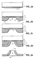
- Figures 1a-e and 2a-e show different manufacturing processes for three dimensional nozzle orifice plates.
- these processes allow electroforming of relatively pure metal or an alloy for manufacturing orifice plates which can be used for thermal inkjet printheads.
- Figures 1e and 2e show nozzle plates having a three dimensional type of nozzle configuration.
- the performance of an inkjet printhead which includes such a nozzle plate allows high quality printing.
- the nozzle protrudes from the orifice surface.
- the outlet opening of the nozzle is separated from the inlet opening of the nozzle by a distance which is greater than the thickness of the nozzle plate.
- the nozzle plate can comprise an electro-deposited metal layer and the interior surface of the nozzle can comprise an electroformed surface of the electro-deposited layer.
- the electro-deposited layer can comprise nickel and the interior surface of the nozzle can comprise a very smooth and converging surface which is frustoconical in shape.
- the mandrel for such three dimensional nozzle orifice plates can comprise a thin film mandrel such as a sheet of nickel which has a configuration suitable for manufacturing of orifice plates having convergent orifices.
- the nickel surface can be coated by nickel or a stainless steel thin film which will serve as an electroforming surface.
- the other portions of the mandrel surface can be coated with a non-conducting material such as a photoresist or plating tape.
- An electroforming process is carried out until the desired thickness is achieved for the orifice plates. Upon separation of the electroformed deposit from the mandrel, three dimensional nozzle orifice plates are obtained.
- a substrate 1 such as polished glass is coated with a conductive film layer 2.
- the conductive film layer 2 can comprise a single layer or multiple layers such as a first layer of chromium which bonds firmly to the substrate 1 and a second layer of stainless steel on the chromium layer.
- the conductive film layer 2 can be provided by a vacuum deposition process such as the planar magnetron process.
- the conductive film layer 2 is patterned by a suitable process such as photolithography. For instance, a photoresist layer can be provided on the conductive film layer 2, a photomask can be placed on the photoresist layer and the photoresist layer can be exposed to ultra violet light.
- the photoresist layer can be developed to obtain the photomask pattern into the photoresist layer and the unmasked areas can be etched to provide a patterned conductive film layer 2 which includes features to be incorporated into a nozzle plate which is electroformed on the mandrel.
- the patterned conductive layer 2 can include an opening 3 extending through the conductive layer 2 to the substrate 1.
- the first type of mandrel allows a nozzle plate to be electroformed such that an outlet opening of a nozzle is formed adjacent the substrate 1.
- a layer of conductive material 4 is deposited on the conductive film layer 2 such that the opening 3 is defined in part by the substrate 1.
- the layer 4 preferably comprises an electro-deposited layer of nickel that extends from the conductive layer 2 such that the opening 3 converges towards the substrate 1.
- the layer 4 provides a pattern 4a of electrically conductive surfaces.
- a release means 5 is provided on the layer 4 to facilitate removal of an electroformed nozzle plate subsequently formed on the pattern 4a of electrically conductive surfaces.
- the release means 5 comprises an oxidized film on the layer 4.
- the oxidized film 5 can be provided by oxidizing the pattern 4a of electrically conductive surfaces.
- an oxygen plasma process can be used to provide the oxidized film 5.
- the release means 5 can comprise a nickel oxide surface of about 10 to 100 ⁇ in thickness on the layer 4.
- Another way of providing the oxidized film 5 is by immersing the layer 4 in a hot bath containing at least one hydroxide of an alkaline earth metal.
- the bath can comprise potassium hydroxide (KOH) which is heated to 80°C and the layer 4 can be immersed for about two hours.
- KOH potassium hydroxide
- the KOH bath can form an oxide and a hydroxide containing layer on the pattern 4a of conductive surfaces.
- the release means 5 reduces adhesion of a subsequently applied electroplated film to the pattern 4a of conductive surfaces.
- a material 6 is deposited on the layer 4 and the release means 5 allows easy separation of the material 6 in the form of a nozzle plate, as shown in Figure 1e.
- the nozzle plate 6 is preferably an electro-deposited layer of nickel and includes an inlet opening 6a and an outlet opening 6b.
- a substrate 7 such as polished glass is coated with a conductive film layer 8.
- the conductive film layer 8 can comprise a single layer or multiple layers such as a first layer of chromium which bonds firmly to the substrate 7 and a second layer of stainless steel on the chromium layer.
- the conductive film layer 8 can be provided by a vacuum deposition process such as the planar magnetron process.
- a dielectric layer 9 such as silicon nitride, silicon carbide or other dielectric material is provided on the conductive film layer 8.
- the dielectric layer 9 can be provided by a suitable process such as a plasma enhanced chemical vapor deposition process and is patterned by a suitable process such as photolithography.
- a photoresist layer can be provided on the dielectric layer 9, a photomask can be placed on the photoresist layer and the photoresist layer can be exposed to ultra violet light.
- the photoresist layer can be developed to obtain the photomask pattern into the photoresist layer and the unmasked areas can be etched to provide a patterned dielectric layer 9 which defines a pattern of electrically conductive regions on the conductive layer 8.
- the patterned dielectric layer 9 can form a region 10 surrounded by exposed portions of the conductive layer 8.
- the second type of mandrel allows a nozzle plate to be electroformed such that an outlet opening of a nozzle is formed adjacent the dielectric layer 9 and thus the height of the nozzle from an inlet opening to an outlet opening of the nozzle can be controlled to be less than that of the nozzle plate 6 formed on the first type of mandrel.
- a layer of conductive material 11 is deposited on the conductive film layer 8 such that the region 10 forms an opening defined in part by the dielectric layer 9.
- the layer 11 preferably comprises an electro-deposited layer of nickel which extends from the conductive layer 8 such that the opening 10 converges towards the dielectric layer 9.
- the layer 11 provides a pattern 11a of electrically conductive surfaces.
- a release means 12 is provided on the layer 11 to facilitate removal of an electroformed nozzle plate subsequently formed on the pattern 11a of electrically conductive surfaces.
- the release means 12 comprises an oxidized film on the layer 11.
- the oxidized film 12 can be provided by oxidizing the pattern 11a of electrically conductive surfaces.
- an oxygen plasma process can be used to provide the oxidized film 12.
- the release means 12 can comprise a nickel oxide surface of about 10 to 100 ⁇ in thickness on the layer 11.
- Another way of providing the oxidized film 12 is by immersing the layer 11 in a hot bath containing at least one hydroxide of an alkaline earth metal.
- the bath can comprise potassium hydroxide (KOH) which is heated to 80°C and the layer 11 can be immersed for about two hours.
- KOH potassium hydroxide
- the KOH bath can form an oxide and a hydroxide containing layer on the pattern 11a of conductive surfaces.
- the release means 12 reduces adhesion of a subsequently applied electroplated film to the pattern 11a of conductive surfaces.
- a material 13 is deposited on the layer 11 and the release means 12 allows easy separation of the material 13 in the form of a nozzle plate, as shown in Figure 2e.
- the nozzle plate 13 is preferably an electro-deposited layer of nickel and includes a nozzle having an inlet opening 13a and an outlet opening 13b with a smooth converging surface extending therebetween.
- the inlet and outlet openings can be spaced apart by a distance which is more than the thickness of the nozzle plate. In fact, this distance could be two or more times larger than the nozzle plate thickness.
- Advantages of the first and second types of mandrels include precise control of the diameter of the nozzle opening, very smooth contour of the inner surface forming the nozzle opening and independent control of the height from the exit surface to the entrance surface. As a result, trajectory of the ink drop as it exits the nozzle opening can be controlled and high quality printing can be obtained.
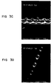
- Figures 3a-f show features of a nozzle plate electroformed on one of the previously described mandrels having the release means 5, 12.
- a nozzle has been formed by electrical discharge machining with an annular electrode to form the outer configuration of the nozzle and a wire to form the opening of the nozzle.
- the nozzle opening described in the article entitled "Air-Assisted Ink Jet with Mesa-Shaped Ink-Drop-Forming Orifice” by Hue Le et al., The 4th International Congress on Advances in Non-Impact Printing Technologies, New La, LA, March 1988 would have a cylindrical rather than a converging surface extending from the inlet opening to the outlet opening thereof. Also, this surface would be expected to exhibit surface roughness.
- the interior surface of the nozzle openings shown in Figures 3a-f is much smoother than the interior surface of the nozzle opening described in the Le et al. article. Accordingly, the nozzle plate of Figures 3a-f will provide more precise control of the inkjet and much higher quality printing than would be obtainable with a nozzle plate having openings like the one described in the Le et al. article.
- the nozzle plates shown in Figures 3a-f allow high quality printing patterns to be obtained having well defined ink drop formations as shown in Figures 4a and 4b. It can be seen from Figures 4a and 4b that the ink drops can be deposited in patterns which have well-defined contours along the edges thereof.
Landscapes
- Engineering & Computer Science (AREA)
- Manufacturing & Machinery (AREA)
- Chemical & Material Sciences (AREA)
- Materials Engineering (AREA)
- Chemical Kinetics & Catalysis (AREA)
- Electrochemistry (AREA)
- Metallurgy (AREA)
- Organic Chemistry (AREA)
- Particle Formation And Scattering Control In Inkjet Printers (AREA)
- Nozzles (AREA)
Claims (20)
- Dünnfilm-Verfahren zum Bilden einer Form (1, 2, 4, 5; 7, 8, 9, 11, 12) zum Herstellen von Tintenstrahl-Düsenplatten und dergleichen, mit folgenden Verfahrensschritten:einem ersten Schritt, bei dem eine elektrisch leitende Schicht (2,8) auf einem im wesentlichen flachen Substrat (1,7) vorgesehen wird;einem zweiten Schritt, bei dem ein Muster aus elektrisch leitenden Oberflächen (4a, 11a) auf der leitenden Schicht (2, 8) vorgesehen wird, wobei mit dem Oberflächenmuster (4a, 11a) die Düsenplatte mit Düsen ausgebildet werden kann, die eine Höhe haben, welche größer ist als die Dicke der Düsenplatte; undeinem dritten Schritt, bei dem die Oberfläche des Musters aus leitenden Oberflächen (4a, 11a) behandelt wird, um die Haftung zwischen einem nachfolgend galvanisch aufgebrachten Film (6, 13) und dem Muster aus leitenden Oberflächen (4a, 11a) zu vermindern.
- Verfahren nach Anspruch 1, bei dem das Substrat (1, 7) Glas umfaßt, der zweite Schritt das Ätzen der elektrisch leitenden Schicht (2, 8) umfaßt, um ein Muster aus elektrisch leitenden Bereichen auf dem Glas auszubilden, und daß galvanische Aufbringen einer zweiten elektrisch leitenden Schicht (4, 11) auf die leitenden Bereiche umfaßt, um das Muster aus elektrisch leitenden Oberflächen (4a, 11a) zu bilden.
- Verfahren nach Anspruch 1, bei dem der zweite Schritt das Vorsehen eines dielektrischen Materials (9) auf der leitenden Schicht (8) umfaßt, um ein Muster aus elektrisch leitenden Bereichen auf der leitenden Schicht (8) zu definieren, und das galvanische Aufbringen einer zweiten elektrisch leitenden Schicht (11) auf die leitenden Bereiche umfaßt, um das Muster aus leitenden Oberflächen (11a) zu bilden.
- Verfahren nach Anspruch 2, bei dem die zweite elektrisch leitende Schicht (4, 11) Nickel aufweist.
- Verfahren nach Anspruch 3, bei dem die zweite elektrisch leitende Schicht (4, 11) Nickel aufweist.
- Verfahren nach Anspruch 1, bei dem der dritte Schritt das Oxidieren des Musters aus leitenden Oberflächen (4a, 11a) umfaßt.
- Verfahren nach Anspruch 6, bei dem in dem Oxidierungsschritt das Muster aus leitenden Oberflächen (4a, 11a) einem Sauerstoff-Plasma-Prozeß ausgesetzt wird.
- Verfahren nach Anspruch 6, bei dem bei dem Oxidierungsschritt das Muster aus leitenden Oberflächen (4a, 11a) in ein heißes Bad eingetaucht wird, welches wenigstens ein Hydroxid aus einem alkalischen Erdmetall aufweist.
- Verfahren nach Anspruch 8, bei dem das Hydroxid Kaliumhydroxid umfaßt.
- Düsenplatte (6, 13) für ein Tintenstrahldrucker, mit: einer Metallplatte ( 6, 13), welche eine erste und eine zweite gegenüberliegende Oberfläche und mehrere Düsen aufweist, von denen jede durch eine Einlaßöffnung (6a, 13a), die sich in die erste Oberfläche hinein erstreckt, und eine Auslaßöffnung (6b, 13b), welche sich in die zweite Öffnung hinein erstreckt, definiert ist, wobei jede Düse eine Innenfläche hat, die von der Einlaßöffnung (6a, 13a) zur Auslaßöffnung (6b, 13b) konvergiert, und wobei die Höhe der Düse von der Einlaßöffnung zu der Auslaßöffnung größer ist als die Dicke der Metallplatte (6, 13), so daß die Düse aus der Ebene der Platte austritt, und wobei die Dicke der Metallplatte von der Einlaßöffnung bis zur Auslaßöffnung im wesentlichen gleichmäßig ist.
- Düsenplatte nach Anspruch 10, bei der die Metallplatte (6, 13) eine galvanisch aufgebrachte Metallschicht aufweist und die innere Oberfläche der Düse eine galvano-plastisch hergestellte Oberfläche auf der galvanisch aufgebrachten Schicht aufweist.
- Düsenplatte nach Anspruch 11, bei der die Metallschicht Nickel umfaßt und die innere Oberfläche der Düse eine glatte und konvergierende Oberfläche mit der Form eines Kegelstumpfs aufweist.
- Form (1, 2, 4, 5; 7, 8, 9, 11, 12) zum Herstellen von Tintenstrahl-Düsenplatten und dergleichen miteinem im wesentlichen flachen Substrat (1, 7);einem Muster aus elektrisch leitenden Oberflächen (4a, 11a) auf dem Substrat (1, 7) zum Ausbilden der Düsenplatte mit Düsen, deren Höhe größer ist als die Dicke der Düsenplatte; undTrennmitteln (5, 12), welche auf dem Muster aus leitenden Oberflächen (4a, 11a) ausgebildet sind, um die Haftung zwischen einem galvanisch aufgebrachten Film (6, 13) und dem Muster aus leitenden Oberflächen (4a, 11a) zu vermindern.
- Form nach Anspruch 13, bei der das Substrat (1, 7) Glas aufweist, das Muster aus leitenden Oberflächen (4a, 11a) eine Nickelschicht aufweist und die Trennmittel (5, 12) wenigstens eine Oberflächenschicht aus Nickeloxid oder Nickelhydroxid auf der Nickelschicht aufweisen.
- Form nach Anspruch 13, bei der das Muster aus leitenden Oberflächen (4a, 11a) eine gemusterte Schicht aus einem elektrisch leitenden Werkstoff (2, 8) auf dem Substrat und eine galvanisch aufgebrachte Schicht (4, 11) aus Nickel auf der Schicht aus dem leitenden Material (4, 11) aufweist, und bei die Trennmittel (5, 12) wenigstens einen Film aus Nickeloxid oder Nickelhydroxid auf der Nickelschicht aufweisen.
- Form nach Anspruch 13, bei der das Muster aus leitenden Oberflächen (4a, 11a) eine Schicht aus einem elektrisch leitenden Werkstoff (8) auf dem Substrat (7), eine Schicht aus einem dielektrischen Werkstoff (9) auf der Schicht aus dem leitenden Werkstoff (8) und eine galvanisch aufgebrachte Schicht (11) aus Nickel auf den freiliegenden Teilen der Schicht aus dem leitenden Werkstoff (8) aufweist.
- Verfahren zum galvanischen Herstellen einer Tintenstrahl-Düsenplatte (6, 13), mit folgenden Verfahrensschritten:einem ersten Schritt, bei dem ein Werkstoff (13), auf einer Oberfläche (4a, 11a) einer Nickelform (1, 2, 4, 5; 7, 8, 9, 11, 12) aufgebracht wird, wobei die Oberfläche (4a, 11a) wenigstens einen Film (5, 12) aus Nickeloxid oder Nickelhydroxid darauf aufweist, um die Haftung des aufgebrachten Werkstoffs (6, 13) an der Nickelform (1, 2, 4, 5; 7, 8, 9, 11, 12) zu vermindern, und wobei die Oberfläche (4a, 11a) ein Muster zum Ausbilden der Düsenplatte mit Düsen, deren Höhe größer ist als die Dicke der Düsenplatte, aufweist; undeinem zweiten Schritt, bei dem der aufgebrachte Werkstoff (6, 13) von der Nickelform (1, 2, 4, 5; 7, 8, 9, 11, 12) getrennt wird, um die Düsenplatte (6, 13) vorzusehen.
- Verfahren nach Anspruch 17, bei dem die Nickelform (1, 2, 4, 5; 7, 8, 9, 11, 12) eine gemusterte Schicht aus einem elektrisch leitenden Werkstoff (2, 8) auf einem Substrat (1, 7) und eine Schicht (4, 11) aus galvanisch aufgebrachtem Nickel auf der Schicht aus dem leitenden Werkstoff (2, 8) aufweist.
- Verfahren nach Anspruch 17, bei dem die Nickelform (7, 8, 9, 11, 12) eine Schicht aus einem elektrisch leitenden Werkstoff (8) aus einem Substrat (7), ein Muster aus einem dielektrischen Werkstoff (9) auf der Schicht aus dem leitenden Werkstoff (8) und eine Schicht aus galvanisch aufgebrachten Nickel (11) auf den freiliegenden Teilen der Schicht aus dem leitenden Werkstoff (8) aufweist.
- Verfahren nach Anspruch 17, bei dem der erste Schritt das galvanische Aufbringen von Nickel als den aufgebrachten Werkstoff (6, 13) umfaßt.
Applications Claiming Priority (2)
| Application Number | Priority Date | Filing Date | Title |
|---|---|---|---|
| US07/621,506 US5255017A (en) | 1990-12-03 | 1990-12-03 | Three dimensional nozzle orifice plates |
| US621506 | 1990-12-03 |
Publications (3)
| Publication Number | Publication Date |
|---|---|
| EP0489246A2 EP0489246A2 (de) | 1992-06-10 |
| EP0489246A3 EP0489246A3 (en) | 1993-03-03 |
| EP0489246B1 true EP0489246B1 (de) | 1996-11-20 |
Family
ID=24490442
Family Applications (1)
| Application Number | Title | Priority Date | Filing Date |
|---|---|---|---|
| EP91117736A Expired - Lifetime EP0489246B1 (de) | 1990-12-03 | 1991-10-17 | Herstellungsverfahren für dreidimensionale Düsenplatten |
Country Status (4)
| Country | Link |
|---|---|
| US (1) | US5255017A (de) |
| EP (1) | EP0489246B1 (de) |
| JP (1) | JPH05193143A (de) |
| DE (1) | DE69123224T2 (de) |
Families Citing this family (30)
| Publication number | Priority date | Publication date | Assignee | Title |
|---|---|---|---|---|
| US5443713A (en) * | 1994-11-08 | 1995-08-22 | Hewlett-Packard Corporation | Thin-film structure method of fabrication |
| CN1072116C (zh) * | 1995-04-14 | 2001-10-03 | 佳能株式会社 | 液体喷射头的制作方法 |
| US5617631A (en) * | 1995-07-21 | 1997-04-08 | Xerox Corporation | Method of making a liquid ink printhead orifice plate |
| US6371596B1 (en) | 1995-10-25 | 2002-04-16 | Hewlett-Packard Company | Asymmetric ink emitting orifices for improved inkjet drop formation |
| US6123413A (en) * | 1995-10-25 | 2000-09-26 | Hewlett-Packard Company | Reduced spray inkjet printhead orifice |
| US6254219B1 (en) | 1995-10-25 | 2001-07-03 | Hewlett-Packard Company | Inkjet printhead orifice plate having related orifices |
| US5901425A (en) | 1996-08-27 | 1999-05-11 | Topaz Technologies Inc. | Inkjet print head apparatus |
| US6145963A (en) * | 1997-08-29 | 2000-11-14 | Hewlett-Packard Company | Reduced size printhead for an inkjet printer |
| US6154234A (en) * | 1998-01-09 | 2000-11-28 | Hewlett-Packard Company | Monolithic ink jet nozzle formed from an oxide and nitride composition |
| CA2330950A1 (en) | 1998-05-12 | 1999-11-18 | E Ink Corporation | Microencapsulated electrophoretic electrostatically-addressed media for drawing device applications |
| CH694453A5 (de) * | 1998-07-24 | 2005-01-31 | Genspec Sa | Mikromechanisch hergestellte Düse zur Erzeugung reproduzierbarer Tröpfchen. |
| US6262833B1 (en) | 1998-10-07 | 2001-07-17 | E Ink Corporation | Capsules for electrophoretic displays and methods for making the same |
| US6402296B1 (en) | 1998-10-29 | 2002-06-11 | Hewlett-Packard Company | High resolution inkjet printer |
| RU2151066C1 (ru) | 1998-11-03 | 2000-06-20 | Самсунг Электроникс Ко., Лтд. | Узел пластины сопла микроинжектора и способ его изготовления |
| CA2365847A1 (en) | 1999-04-06 | 2000-10-12 | Gregg M. Duthaler | Methods for producing droplets for use in capsule-based electrophoretic displays |
| JP2001113698A (ja) * | 1999-10-19 | 2001-04-24 | Nec Niigata Ltd | ノズルプレート及びその製造方法及びインクジェット記録ヘッド |
| US20050156340A1 (en) | 2004-01-20 | 2005-07-21 | E Ink Corporation | Preparation of capsules |
| US6790325B2 (en) * | 2001-04-09 | 2004-09-14 | Hewlett-Packard Development Company, L.P. | Re-usable mandrel for fabrication of ink-jet orifice plates |
| US6533394B1 (en) * | 2001-08-29 | 2003-03-18 | Hewlett-Packard Company | Orifice plate with break tabs and method of manufacturing |
| US20030143492A1 (en) | 2002-01-31 | 2003-07-31 | Scitex Digital Printing, Inc. | Mandrel with controlled release layer for multi-layer electroformed ink jet orifice plates |
| US8162966B2 (en) * | 2002-10-25 | 2012-04-24 | Hydrocision, Inc. | Surgical devices incorporating liquid jet assisted tissue manipulation and methods for their use |
| US10363061B2 (en) | 2002-10-25 | 2019-07-30 | Hydrocision, Inc. | Nozzle assemblies for liquid jet surgical instruments and surgical instruments for employing the nozzle assemblies |
| US7040016B2 (en) * | 2003-10-22 | 2006-05-09 | Hewlett-Packard Development Company, L.P. | Method of fabricating a mandrel for electroformation of an orifice plate |
| JP4924803B2 (ja) * | 2006-03-28 | 2012-04-25 | ブラザー工業株式会社 | インクジェット記録用水性インク |
| DE102011089701A1 (de) | 2011-12-22 | 2013-06-27 | Lufthansa Technik Ag | Vorrichtung zum Rekonturieren einer Gasturbinenschaufel |
| DE102013002413A1 (de) * | 2013-02-11 | 2014-08-14 | Dürr Systems GmbH | Lochplatte für ein Applikationsgerät und entsprechendes Applikations- und Herstellungsverfahren |
| EP3231898B1 (de) * | 2014-12-12 | 2019-10-09 | Citizen Watch Co., Ltd. | Verfahren zur herstellung von elektrogeformten komponenten |
| US10485568B2 (en) | 2016-06-24 | 2019-11-26 | Hydrocision, Inc. | Selective tissue removal treatment device |
| US10492821B2 (en) | 2016-06-24 | 2019-12-03 | Hydrocision, Inc. | Selective tissue removal treatment device |
| US11380557B2 (en) * | 2017-06-05 | 2022-07-05 | Applied Materials, Inc. | Apparatus and method for gas delivery in semiconductor process chambers |
Family Cites Families (7)
| Publication number | Priority date | Publication date | Assignee | Title |
|---|---|---|---|---|
| US2870068A (en) * | 1956-01-30 | 1959-01-20 | Diamond Gardner Corp | Electroformed screens |
| FR2363643A1 (fr) * | 1976-09-01 | 1978-03-31 | Duchenaud Alain | Procede et dispositif pour la fabrication d'un cylindre a paroi epaisse perforee et cylindre obtenu |
| US4528070A (en) * | 1983-02-04 | 1985-07-09 | Burlington Industries, Inc. | Orifice plate constructions |
| IT1182402B (it) * | 1985-02-04 | 1987-10-05 | Olivetti & Co Spa | Metodo id fabbricazione di elementi metallici di stampa a getto d inchiostro e relativi elementi di stampa |
| US4773971A (en) * | 1986-10-30 | 1988-09-27 | Hewlett-Packard Company | Thin film mandrel |
| US4801947A (en) * | 1987-06-25 | 1989-01-31 | Burlington Industries, Inc. | Electrodeposition-produced orifice plate of amorphous metal |
| US4954225A (en) * | 1990-01-10 | 1990-09-04 | Dynamics Research Corporation | Method for making nozzle plates |
-
1990
- 1990-12-03 US US07/621,506 patent/US5255017A/en not_active Expired - Fee Related
-
1991
- 1991-10-17 DE DE69123224T patent/DE69123224T2/de not_active Expired - Fee Related
- 1991-10-17 EP EP91117736A patent/EP0489246B1/de not_active Expired - Lifetime
- 1991-12-03 JP JP3348000A patent/JPH05193143A/ja active Pending
Also Published As
| Publication number | Publication date |
|---|---|
| DE69123224D1 (de) | 1997-01-02 |
| EP0489246A3 (en) | 1993-03-03 |
| DE69123224T2 (de) | 1997-06-12 |
| EP0489246A2 (de) | 1992-06-10 |
| JPH05193143A (ja) | 1993-08-03 |
| US5255017A (en) | 1993-10-19 |
Similar Documents
| Publication | Publication Date | Title |
|---|---|---|
| EP0489246B1 (de) | Herstellungsverfahren für dreidimensionale Düsenplatten | |
| US4954225A (en) | Method for making nozzle plates | |
| EP0485182B1 (de) | Thermischer Dünnschichttintenstrahldruckkopf mit einer plastischen Düsenplatte und Herstellungsverfahren | |
| US5167776A (en) | Thermal inkjet printhead orifice plate and method of manufacture | |
| EP0629504B1 (de) | Düsenplatte für Tintenstrahldrucker | |
| EP0249625B1 (de) | Tintenstrahlschutzschicht und lochplattedruckkopf und herstellung | |
| US5236572A (en) | Process for continuously electroforming parts such as inkjet orifice plates for inkjet printers | |
| US4675083A (en) | Compound bore nozzle for ink jet printhead and method of manufacture | |
| CA1302161C (en) | Nozzle plate geometry for ink jet pens and method of manufacture | |
| JPS59118469A (ja) | プリントヘツド | |
| EP1221375A2 (de) | Düsenplatte für Tintenstrahldruckkopf | |
| US6238584B1 (en) | Method of forming ink jet nozzle plates | |
| US7437820B2 (en) | Method of manufacturing a charge plate and orifice plate for continuous ink jet printers | |
| US7552534B2 (en) | Method of manufacturing an integrated orifice plate and electroformed charge plate | |
| EP1002647A2 (de) | Verfahren und Vorrichtung zur Elektroformung für eine Tintenstrahldüsenplatte | |
| US7540589B2 (en) | Integrated charge and orifice plates for continuous ink jet printers | |
| JP3166830B2 (ja) | 静電吸引型マルチノズルインクジェットヘッドの製造方法 | |
| CA1303903C (en) | Barrier layer and orifice plate for thermal ink jet print head assemblyand method of manufacture | |
| JPH07256885A (ja) | インクジェット記録装置のインク吐出口の製作方法 | |
| JPH06286141A (ja) | インクジェットヘッド用ノズル板の製造方法 |
Legal Events
| Date | Code | Title | Description |
|---|---|---|---|
| PUAI | Public reference made under article 153(3) epc to a published international application that has entered the european phase |
Free format text: ORIGINAL CODE: 0009012 |
|
| AK | Designated contracting states |
Kind code of ref document: A2 Designated state(s): DE FR GB IT |
|
| PUAL | Search report despatched |
Free format text: ORIGINAL CODE: 0009013 |
|
| AK | Designated contracting states |
Kind code of ref document: A3 Designated state(s): DE FR GB IT |
|
| 17P | Request for examination filed |
Effective date: 19930602 |
|
| 17Q | First examination report despatched |
Effective date: 19940509 |
|
| GRAG | Despatch of communication of intention to grant |
Free format text: ORIGINAL CODE: EPIDOS AGRA |
|
| GRAH | Despatch of communication of intention to grant a patent |
Free format text: ORIGINAL CODE: EPIDOS IGRA |
|
| GRAH | Despatch of communication of intention to grant a patent |
Free format text: ORIGINAL CODE: EPIDOS IGRA |
|
| GRAA | (expected) grant |
Free format text: ORIGINAL CODE: 0009210 |
|
| AK | Designated contracting states |
Kind code of ref document: B1 Designated state(s): DE FR GB IT |
|
| REF | Corresponds to: |
Ref document number: 69123224 Country of ref document: DE Date of ref document: 19970102 |
|
| ITF | It: translation for a ep patent filed | ||
| ET | Fr: translation filed | ||
| PLBE | No opposition filed within time limit |
Free format text: ORIGINAL CODE: 0009261 |
|
| STAA | Information on the status of an ep patent application or granted ep patent |
Free format text: STATUS: NO OPPOSITION FILED WITHIN TIME LIMIT |
|
| 26N | No opposition filed | ||
| PGFP | Annual fee paid to national office [announced via postgrant information from national office to epo] |
Ref country code: FR Payment date: 19980930 Year of fee payment: 8 |
|
| PGFP | Annual fee paid to national office [announced via postgrant information from national office to epo] |
Ref country code: GB Payment date: 19981015 Year of fee payment: 8 |
|
| PG25 | Lapsed in a contracting state [announced via postgrant information from national office to epo] |
Ref country code: GB Free format text: LAPSE BECAUSE OF NON-PAYMENT OF DUE FEES Effective date: 19991017 |
|
| GBPC | Gb: european patent ceased through non-payment of renewal fee |
Effective date: 19991017 |
|
| PG25 | Lapsed in a contracting state [announced via postgrant information from national office to epo] |
Ref country code: FR Free format text: LAPSE BECAUSE OF NON-PAYMENT OF DUE FEES Effective date: 20000630 |
|
| REG | Reference to a national code |
Ref country code: FR Ref legal event code: ST |
|
| PGFP | Annual fee paid to national office [announced via postgrant information from national office to epo] |
Ref country code: DE Payment date: 20000925 Year of fee payment: 10 |
|
| PG25 | Lapsed in a contracting state [announced via postgrant information from national office to epo] |
Ref country code: DE Free format text: LAPSE BECAUSE OF NON-PAYMENT OF DUE FEES Effective date: 20020702 |
|
| PG25 | Lapsed in a contracting state [announced via postgrant information from national office to epo] |
Ref country code: IT Free format text: LAPSE BECAUSE OF NON-PAYMENT OF DUE FEES;WARNING: LAPSES OF ITALIAN PATENTS WITH EFFECTIVE DATE BEFORE 2007 MAY HAVE OCCURRED AT ANY TIME BEFORE 2007. THE CORRECT EFFECTIVE DATE MAY BE DIFFERENT FROM THE ONE RECORDED. Effective date: 20051017 |