EP0489512A2 - Circuit de sonnerie pour téléphone - Google Patents
Circuit de sonnerie pour téléphone Download PDFInfo
- Publication number
- EP0489512A2 EP0489512A2 EP91310581A EP91310581A EP0489512A2 EP 0489512 A2 EP0489512 A2 EP 0489512A2 EP 91310581 A EP91310581 A EP 91310581A EP 91310581 A EP91310581 A EP 91310581A EP 0489512 A2 EP0489512 A2 EP 0489512A2
- Authority
- EP
- European Patent Office
- Prior art keywords
- ringer
- output
- transformer
- current
- feedback loop
- Prior art date
- Legal status (The legal status is an assumption and is not a legal conclusion. Google has not performed a legal analysis and makes no representation as to the accuracy of the status listed.)
- Withdrawn
Links
Images
Classifications
-
- H—ELECTRICITY
- H03—ELECTRONIC CIRCUITRY
- H03K—PULSE TECHNIQUE
- H03K17/00—Electronic switching or gating, i.e. not by contact-making and –breaking
- H03K17/51—Electronic switching or gating, i.e. not by contact-making and –breaking characterised by the components used
- H03K17/56—Electronic switching or gating, i.e. not by contact-making and –breaking characterised by the components used by the use, as active elements, of semiconductor devices
- H03K17/687—Electronic switching or gating, i.e. not by contact-making and –breaking characterised by the components used by the use, as active elements, of semiconductor devices the devices being field-effect transistors
- H03K17/689—Electronic switching or gating, i.e. not by contact-making and –breaking characterised by the components used by the use, as active elements, of semiconductor devices the devices being field-effect transistors with galvanic isolation between the control circuit and the output circuit
- H03K17/691—Electronic switching or gating, i.e. not by contact-making and –breaking characterised by the components used by the use, as active elements, of semiconductor devices the devices being field-effect transistors with galvanic isolation between the control circuit and the output circuit using transformer coupling
-
- H—ELECTRICITY
- H03—ELECTRONIC CIRCUITRY
- H03M—CODING; DECODING; CODE CONVERSION IN GENERAL
- H03M1/00—Analogue/digital conversion; Digital/analogue conversion
-
- H—ELECTRICITY
- H02—GENERATION; CONVERSION OR DISTRIBUTION OF ELECTRIC POWER
- H02M—APPARATUS FOR CONVERSION BETWEEN AC AND AC, BETWEEN AC AND DC, OR BETWEEN DC AND DC, AND FOR USE WITH MAINS OR SIMILAR POWER SUPPLY SYSTEMS; CONVERSION OF DC OR AC INPUT POWER INTO SURGE OUTPUT POWER; CONTROL OR REGULATION THEREOF
- H02M7/00—Conversion of AC power input into DC power output; Conversion of DC power input into AC power output
- H02M7/42—Conversion of DC power input into AC power output without possibility of reversal
- H02M7/44—Conversion of DC power input into AC power output without possibility of reversal by static converters
- H02M7/48—Conversion of DC power input into AC power output without possibility of reversal by static converters using discharge tubes with control electrode or semiconductor devices with control electrode
- H02M7/53—Conversion of DC power input into AC power output without possibility of reversal by static converters using discharge tubes with control electrode or semiconductor devices with control electrode using devices of a triode or transistor type requiring continuous application of a control signal
- H02M7/537—Conversion of DC power input into AC power output without possibility of reversal by static converters using discharge tubes with control electrode or semiconductor devices with control electrode using devices of a triode or transistor type requiring continuous application of a control signal using semiconductor devices only, e.g. single switched pulse inverters
- H02M7/538—Conversion of DC power input into AC power output without possibility of reversal by static converters using discharge tubes with control electrode or semiconductor devices with control electrode using devices of a triode or transistor type requiring continuous application of a control signal using semiconductor devices only, e.g. single switched pulse inverters in a push-pull configuration
- H02M7/53803—Conversion of DC power input into AC power output without possibility of reversal by static converters using discharge tubes with control electrode or semiconductor devices with control electrode using devices of a triode or transistor type requiring continuous application of a control signal using semiconductor devices only, e.g. single switched pulse inverters in a push-pull configuration with automatic control of output voltage or current
-
- H—ELECTRICITY
- H03—ELECTRONIC CIRCUITRY
- H03K—PULSE TECHNIQUE
- H03K17/00—Electronic switching or gating, i.e. not by contact-making and –breaking
- H03K17/51—Electronic switching or gating, i.e. not by contact-making and –breaking characterised by the components used
- H03K17/56—Electronic switching or gating, i.e. not by contact-making and –breaking characterised by the components used by the use, as active elements, of semiconductor devices
- H03K17/687—Electronic switching or gating, i.e. not by contact-making and –breaking characterised by the components used by the use, as active elements, of semiconductor devices the devices being field-effect transistors
- H03K17/6871—Electronic switching or gating, i.e. not by contact-making and –breaking characterised by the components used by the use, as active elements, of semiconductor devices the devices being field-effect transistors the output circuit comprising more than one controlled field-effect transistor
- H03K17/6872—Electronic switching or gating, i.e. not by contact-making and –breaking characterised by the components used by the use, as active elements, of semiconductor devices the devices being field-effect transistors the output circuit comprising more than one controlled field-effect transistor using complementary field-effect transistors
-
- H—ELECTRICITY
- H04—ELECTRIC COMMUNICATION TECHNIQUE
- H04M—TELEPHONIC COMMUNICATION
- H04M19/00—Current supply arrangements for telephone systems
- H04M19/02—Current supply arrangements for telephone systems providing ringing current or supervisory tones, e.g. dialling tone or busy tone
- H04M19/023—Current supply arrangements for telephone systems providing ringing current or supervisory tones, e.g. dialling tone or busy tone by reversing the polarity of the current at the exchange
Definitions
- the present invention relates to a ringer for use in a telephone network.
- the purpose of a ringer is to provide ring current to indicate to a telephone subscriber that there is an incoming call.
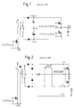
- the ringer provides a low frequency sinusoidal waveform and prior art systems have used primary and secondary high frequency switching stages, such as are shown in Figures 1 and 2.
- a primary stage provides a pair of intermediate voltage rails.
- the secondary stage is pulse width modulated and swings between the two rails.
- the resulting modulated voltage waveform is then filtered to produce the required output waveform.
- Two high frequency switching stages are required which reduce the efficiency and cause high dissipation at maximum load and bulky filtering components are needed.
- the primary stage provides a current source to the secondary stage, which uses high frequency modulation techniques to form the required output voltage.
- the output current and secondary current are compared and used to limit the primary current, reducing excessive power dissipation.
- a ringer for a telephone system comprising a transformer having a first feedback loop controlling in use the primary current of the transformer in response to the ringer output and a second feedback loop controlling in use the secondary current of the transformer in response to the ringer output.
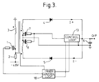
- Figure 3 shows a fly back convertor being used to provide current sources I+ and I- controlled by a secondary switching stage, comprising a pair of MOSFETs 7 and 8.
- the output waveform is controlled by two voltage feedback loops 13,18, giving the circuit two modes of operation.
- an inner control loop 18 will modulate the primary current to maintain the amplitude of the output waveform.
- An outer control loop 13 will keep only one of the pair of MOSFETs 7 and 8 switched on throughout a half cycle of the output waveform, to give the appropriate polarity of supply.
- the secondary current flows in the path selected by a one of the MOSFETs 7 or 8. This charges an output capacitor 6 as appropriate to form the required output waveform. No circulating currents occur during large current demands and high efficiency, reduced power dissipation and reduced noise result.
- the secondary MOSFETs 7 and 8 change from operating as a polarity switch to operating as a high frequency modulator. This is necessary as, without a load current present, the voltage on the output capacitor 6 has no way of discharging during the second half of each half cycle to maintain the sinusoidal output waveform. Circulating currents during these light load conditions are not significantly wasteful.
- the outer control loop 13 contains a potential divider 9, which monitors the output voltage level on the capacitor 6.
- a reference sinewave oscillator 10 and the mid point of the divider 9 are applied to a differential amplifier 11 acting as a comparator. This will produce an output error voltage indicating the difference between the two inputs.
- This output is then synchronized with a clock by a flip-flop 12. This gives a minimum duration of 5 microseconds in any one state, any longer durations are multiples of this basic period.
- the resulting output of the outer control loop 13 is applied as a switching voltage to the gates of a pair of MOSFETs 7 and 8. These are configured so that when one is switched on, the other will be switched off. These MOSFETs provide a path so that the output capacitor 6 can be charged to an appropriate polarity. MOSFET 7 allows positive charging via a diode 4, and MOSFET 8 allows negative charging via a diode 5. The necessary charging current is provided by a fly back transformer 3, whose secondary windings are connected into the appropriate paths. It should be noted that the secondaries inductances and the output capacitor 6, form a low pass filter so that a smooth output voltage waveform results.
- the voltage on the output capacitor 6 has no external discharge path to maintain a sinusoidal output waveform.
- the control loop 13 will vary its duty cycle to maintain the correct voltage on the capacitor 6.
- the inputs to the comparator 11 are easily maintained in balance and therefore idling occurs. This is where charge is supplied to and removed from capacitor 6 many times during a half cycle of the output waveform and circulating currents occur.
- the inputs to the differential amplifier 11 are also applied to an inner control loop 18.
- the output of the amplifier 14 is then applied to a full wave rectifier 15 which produces a unipolar error voltage.
- a voltage controlled current source 16 is then used to provide level shifting to apply an error voltage Ve to a pulse width modulator 17.
- the pulse width modulator 17 turns on a primary MOSFET 1, current then builds up in the primary of the flyback transformer 3. This current is sensed by a resistor 2 and is used to reset the modulator 17 to provide current mode control. The magnitude of the error voltage Ve gives a corresponding pulse width from the modulator 17 and hence defines the peak primary current. This primary current is then transformed to the secondary windings by the flyback action of the transformer 3.
- the output switching stage of MOSFET 7 and 8 is merely a polarity switch and the output amplitude is formed entirely by the inner control loop 18 modulating the primary. This gives good efficiency and hence low dissipation during large ringer current demands.
Landscapes
- Engineering & Computer Science (AREA)
- Power Engineering (AREA)
- Signal Processing (AREA)
- Theoretical Computer Science (AREA)
- Dc-Dc Converters (AREA)
- Devices For Supply Of Signal Current (AREA)
Applications Claiming Priority (2)
| Application Number | Priority Date | Filing Date | Title |
|---|---|---|---|
| GB909026504A GB9026504D0 (en) | 1990-12-05 | 1990-12-05 | Telephone ringer circuit |
| GB9026504 | 1990-12-05 |
Publications (2)
| Publication Number | Publication Date |
|---|---|
| EP0489512A2 true EP0489512A2 (fr) | 1992-06-10 |
| EP0489512A3 EP0489512A3 (en) | 1993-03-24 |
Family
ID=10686559
Family Applications (1)
| Application Number | Title | Priority Date | Filing Date |
|---|---|---|---|
| EP19910310581 Withdrawn EP0489512A3 (en) | 1990-12-05 | 1991-11-15 | Telephone ringer circuit |
Country Status (10)
| Country | Link |
|---|---|
| EP (1) | EP0489512A3 (fr) |
| JP (1) | JPH04340841A (fr) |
| KR (1) | KR920013934A (fr) |
| CN (1) | CN1062061A (fr) |
| AU (1) | AU651398B2 (fr) |
| CA (1) | CA2056132A1 (fr) |
| FI (1) | FI915711A7 (fr) |
| GB (2) | GB9026504D0 (fr) |
| IE (1) | IE914004A1 (fr) |
| PT (1) | PT99681A (fr) |
Cited By (3)
| Publication number | Priority date | Publication date | Assignee | Title |
|---|---|---|---|---|
| DE4218845A1 (de) * | 1992-06-09 | 1993-12-16 | Bosch Telecom | Schaltungsanordnung für einen Rufspannungsgenerator |
| DE19740137A1 (de) * | 1997-09-12 | 1999-03-18 | Alsthom Cge Alcatel | Verfahren und Schaltungsanordnung zur Rufwechselspannungserzeugung für elektronische Teilnehmerschaltungen |
| WO2001089089A2 (fr) | 2000-05-12 | 2001-11-22 | Honeywell International Inc. | Source de courant bidirectionnel |
Family Cites Families (2)
| Publication number | Priority date | Publication date | Assignee | Title |
|---|---|---|---|---|
| GB8606151D0 (en) * | 1986-03-12 | 1986-04-16 | Gen Electric Co Plc | Telephone system circuit |
| US4890210A (en) * | 1988-11-15 | 1989-12-26 | Gilbarco, Inc. | Power supply having combined forward converter and flyback action for high efficiency conversion from low to high voltage |
-
1990
- 1990-12-05 GB GB909026504A patent/GB9026504D0/en active Pending
-
1991
- 1991-11-15 EP EP19910310581 patent/EP0489512A3/en not_active Withdrawn
- 1991-11-15 GB GB9124299A patent/GB2250663B/en not_active Expired - Lifetime
- 1991-11-18 IE IE400491A patent/IE914004A1/en not_active Application Discontinuation
- 1991-11-26 CA CA002056132A patent/CA2056132A1/fr not_active Abandoned
- 1991-12-02 JP JP3343888A patent/JPH04340841A/ja active Pending
- 1991-12-04 KR KR1019910022137A patent/KR920013934A/ko not_active Withdrawn
- 1991-12-04 PT PT99681A patent/PT99681A/pt not_active Application Discontinuation
- 1991-12-04 FI FI915711A patent/FI915711A7/fi not_active Application Discontinuation
- 1991-12-04 AU AU88854/91A patent/AU651398B2/en not_active Ceased
- 1991-12-05 CN CN91111571A patent/CN1062061A/zh active Pending
Cited By (4)
| Publication number | Priority date | Publication date | Assignee | Title |
|---|---|---|---|---|
| DE4218845A1 (de) * | 1992-06-09 | 1993-12-16 | Bosch Telecom | Schaltungsanordnung für einen Rufspannungsgenerator |
| DE19740137A1 (de) * | 1997-09-12 | 1999-03-18 | Alsthom Cge Alcatel | Verfahren und Schaltungsanordnung zur Rufwechselspannungserzeugung für elektronische Teilnehmerschaltungen |
| WO2001089089A2 (fr) | 2000-05-12 | 2001-11-22 | Honeywell International Inc. | Source de courant bidirectionnel |
| WO2001089089A3 (fr) * | 2000-05-12 | 2002-02-28 | Honeywell Int Inc | Source de courant bidirectionnel |
Also Published As
| Publication number | Publication date |
|---|---|
| JPH04340841A (ja) | 1992-11-27 |
| FI915711L (fi) | 1992-06-06 |
| GB2250663B (en) | 1995-04-19 |
| GB2250663A (en) | 1992-06-10 |
| GB9026504D0 (en) | 1991-01-23 |
| PT99681A (pt) | 1994-01-31 |
| KR920013934A (ko) | 1992-07-30 |
| FI915711A7 (fi) | 1992-06-06 |
| GB9124299D0 (en) | 1992-01-08 |
| AU8885491A (en) | 1992-06-11 |
| FI915711A0 (fi) | 1991-12-04 |
| IE914004A1 (en) | 1992-06-17 |
| AU651398B2 (en) | 1994-07-21 |
| CN1062061A (zh) | 1992-06-17 |
| CA2056132A1 (fr) | 1992-06-06 |
| EP0489512A3 (en) | 1993-03-24 |
Similar Documents
| Publication | Publication Date | Title |
|---|---|---|
| US5642267A (en) | Single-stage, unity power factor switching converter with voltage bidirectional switch and fast output regulation | |
| US5859771A (en) | Half/full bridge converter | |
| US4290101A (en) | N Phase digital inverter | |
| EP0066577B1 (fr) | Convertisseur de tension a largeur d'impulsion modulee pour generer de preference une tension alternative sinusoidale | |
| EP0096370B1 (fr) | Dispositif d'alimentation en courant | |
| JP2877164B2 (ja) | インバータ又は直流変圧器のための自己発振スイッチング装置 | |
| EP0553179B1 (fr) | Convertisseur de courant continu en courant alternatif | |
| KR20010040865A (ko) | 개방 루프 직류-교류 컨버터로 사용하기 위한 펄스폭 변조제어기 | |
| US6477062B1 (en) | Power supply unit including an inverter | |
| GB2029989A (en) | Automatic control converters | |
| US5517397A (en) | Flyback power converter with spike compensator circuit | |
| US5307407A (en) | 20 Hz ring generator using high frequency PWM control | |
| JPH11122926A (ja) | 自励発振型スイッチング電源装置 | |
| US4794508A (en) | PWM control circuit for a non-symmetrical switching power supply | |
| US3838329A (en) | Power supply circuit | |
| JP4198379B2 (ja) | Dc/dcコンバータを具えた電源装置 | |
| US8760230B2 (en) | Switching amplifier with pulsed current source and sink | |
| US20130121039A1 (en) | Switching amplifier with pulsed current supply | |
| US5070439A (en) | DC to DC converter apparatus employing push-pull oscillators | |
| EP0489512A2 (fr) | Circuit de sonnerie pour téléphone | |
| JP2000152632A (ja) | ホ―ルドアップ時間を有し高調波を低減した切換電力変換器 | |
| JP2003125582A (ja) | 電源装置 | |
| EP0949751A2 (fr) | Générateur pour machine de soudage à l'arc avec topologie de convertisseur direct et verouillage actif | |
| JPH04113754A (ja) | 任意波形発生装置 | |
| US5682302A (en) | Adaptable power converter applying digitized-wave-generation for integrated circuit implementation |
Legal Events
| Date | Code | Title | Description |
|---|---|---|---|
| PUAI | Public reference made under article 153(3) epc to a published international application that has entered the european phase |
Free format text: ORIGINAL CODE: 0009012 |
|
| AK | Designated contracting states |
Kind code of ref document: A2 Designated state(s): BE DE DK ES FR GR IT LU NL SE |
|
| PUAL | Search report despatched |
Free format text: ORIGINAL CODE: 0009013 |
|
| AK | Designated contracting states |
Kind code of ref document: A3 Designated state(s): BE DE DK ES FR GR IT LU NL SE |
|
| 17P | Request for examination filed |
Effective date: 19930908 |
|
| 17Q | First examination report despatched |
Effective date: 19940713 |
|
| STAA | Information on the status of an ep patent application or granted ep patent |
Free format text: STATUS: THE APPLICATION HAS BEEN WITHDRAWN |
|
| 18W | Application withdrawn |
Withdrawal date: 19950919 |
|
| R18W | Application withdrawn (corrected) |
Effective date: 19950919 |