EP0491375A2 - Système de réalisation de motifs - Google Patents
Système de réalisation de motifs Download PDFInfo
- Publication number
- EP0491375A2 EP0491375A2 EP91121690A EP91121690A EP0491375A2 EP 0491375 A2 EP0491375 A2 EP 0491375A2 EP 91121690 A EP91121690 A EP 91121690A EP 91121690 A EP91121690 A EP 91121690A EP 0491375 A2 EP0491375 A2 EP 0491375A2
- Authority
- EP
- European Patent Office
- Prior art keywords
- wafer
- shot
- pattern
- regions
- matrix
- Prior art date
- Legal status (The legal status is an assumption and is not a legal conclusion. Google has not performed a legal analysis and makes no representation as to the accuracy of the status listed.)
- Granted
Links
Images


Classifications
-
- G—PHYSICS
- G03—PHOTOGRAPHY; CINEMATOGRAPHY; ANALOGOUS TECHNIQUES USING WAVES OTHER THAN OPTICAL WAVES; ELECTROGRAPHY; HOLOGRAPHY
- G03F—PHOTOMECHANICAL PRODUCTION OF TEXTURED OR PATTERNED SURFACES, e.g. FOR PRINTING, FOR PROCESSING OF SEMICONDUCTOR DEVICES; MATERIALS THEREFOR; ORIGINALS THEREFOR; APPARATUS SPECIALLY ADAPTED THEREFOR
- G03F7/00—Photomechanical, e.g. photolithographic, production of textured or patterned surfaces, e.g. printing surfaces; Materials therefor, e.g. comprising photoresists; Apparatus specially adapted therefor
- G03F7/70—Microphotolithographic exposure; Apparatus therefor
- G03F7/70425—Imaging strategies, e.g. for increasing throughput or resolution, printing product fields larger than the image field or compensating lithography- or non-lithography errors, e.g. proximity correction, mix-and-match, stitching or double patterning
- G03F7/70433—Layout for increasing efficiency or for compensating imaging errors, e.g. layout of exposure fields for reducing focus errors; Use of mask features for increasing efficiency or for compensating imaging errors
-
- G—PHYSICS
- G03—PHOTOGRAPHY; CINEMATOGRAPHY; ANALOGOUS TECHNIQUES USING WAVES OTHER THAN OPTICAL WAVES; ELECTROGRAPHY; HOLOGRAPHY
- G03F—PHOTOMECHANICAL PRODUCTION OF TEXTURED OR PATTERNED SURFACES, e.g. FOR PRINTING, FOR PROCESSING OF SEMICONDUCTOR DEVICES; MATERIALS THEREFOR; ORIGINALS THEREFOR; APPARATUS SPECIALLY ADAPTED THEREFOR
- G03F7/00—Photomechanical, e.g. photolithographic, production of textured or patterned surfaces, e.g. printing surfaces; Materials therefor, e.g. comprising photoresists; Apparatus specially adapted therefor
- G03F7/70—Microphotolithographic exposure; Apparatus therefor
- G03F7/70425—Imaging strategies, e.g. for increasing throughput or resolution, printing product fields larger than the image field or compensating lithography- or non-lithography errors, e.g. proximity correction, mix-and-match, stitching or double patterning
- G03F7/70475—Stitching, i.e. connecting image fields to produce a device field, the field occupied by a device such as a memory chip, processor chip, CCD, flat panel display
Definitions
- the present invention relates to a pattern forming system wherein a pattern formed on a reticule is demagnified and projected on a surface of a wafer by a step- and repeat photolithographic system with demagnification (hereinafter called stepper) and an application of such a system to an apparatus for exposing photoresist formed on the wafer in a step and repeat system.
- stepper photolithographic system with demagnification
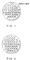
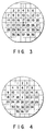
- the first case relates to short regions (1 to 38), and shows that an even number of shot regions in which the patterns formed on the reticule exist in the respective X and Y directions from an origin of the coordinate axes.
- the second case relates to shot regions 1 to 40 and shows that an even number of shot regions exist in the X direction and that an odd number of shot regions exist in the Y direction.
- the third case relates to short regions 1 to 39, and shows that an odd number of short regions exist in the X direction and that an even number of short regions exist in the Y direction.
- the fourth case relates to short regions (1 to 37), and shows that an odd number of shot regions exist in the respective X and Y directions.
- the number of complete patterns to be formed in the wafer will be 38 according to the first case of Fig. 1, 40 according to the second case of Fig. 2, 39 according to the third case of Fig. 3, and 37 according to the fourth case of Fig. 4. Therefore, if the patterns to be formed by one short constitutes one integrated circuit (IC), the maximum number of IC to be obtained from one wafer can be obtained in the array method of the shot regions shown in Fig. 2. In other words, if the patterns on the reticule are formed on the surface of the wafer by use of the array method of the shot regions shown in Fig. 2, the maximum number of ICs can be obtained from one wafer, and efficiency of IC production can be improved.
- IC integrated circuit
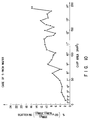
- Fig. 5 shows the relationship between the size of the chip and the gross of the chip gross relating to an experimental value and a theoretical value.
- a theoretical value shown by a broken line of Fig. 5 is a number, which is obtained by dividing an area of a main surface of the wafer by an area of one IC.
- a chip gross shown by a solid line of Fig. 5 is a number of ICs, which are actually formed on the main surface of the wafer in a complete shape if the patterns are formed on the surface of the wafer by a predetermined array method. In other words, if the size of the IC is 3 mm x 3 mm, both the experimental value of the chip gross and the theoretical value are about 1300, respectively. Due to this, it is impossible for workers to count the number of ICs formed on the surface of the wafer one by one.
- An object of the invention is to provide a pattern forming system wherein a pattern formed on a reticule, is demagnified and projected on a surface of a wafer according to an array method in which the number of times of shots is minimized and an array method of shot regions where the number of ICs to be formed on the surface of the wafer is automatically selected in demagnifying and projecting the pattern thereon.
- the pattern forming system of the present invention comprises a reticule on which a pattern is formed on one or more chips, an apparatus for preliminarily arranging a plurality of shot regions on a main surface of a wafer in a matrix manner in a case where regions where the pattern is formed by one shot are used as shot regions, an apparatus for calculating the number of the shot regions, which constitutes the matrix after sequentially moving the position of the shot regions to be a center of the matrix in a state that wafer is fixed, and the number of the chips wherein the pattern is completely formed in the main surface of the wafer, an apparatus for selecting a case in which the number of the shot regions constituting the matrix is the smallest and the number of the chips in which the pattern is completely formed in the main surface of the wafer is the largest, and an apparatus for forming the pattern, which is formed on the reticule, on each shot region constituting the matrix.
- the four cases can be considered to expose photoresist formed on the wafer in the step and repeat system.
- the array method of the regions (shot regions) where one pattern is formed is not limited to the above-mentioned four cases.
- the present invention provides an apparatus for automatically determining an array method of shot regions wherein the number of times of demagnifying and projecting the pattern on the surface of the wafer becomes minimum and the number of the ICs to be formed on one wafer becomes maximum.
- a wafer size WS is selected from either one of 3, 4, 5, or 6 inches.
- a center of the wafer (shown by a mark x of Figs. 6 to 8) is determined, and defined as an origin O.
- an X axis and an Y axis being at a right angle to the X axis are determined based on the origin O, thereby a two-dimensional coordinate system is determined.
- the shot size S means a size of one pattern (shot region) to be formed on the surface of the wafer by one shot.
- the chip size CS means a size of the region to be as one chip formed on the surface of the wafer. In other words, there is a case that a plurality of patterns are formed on the surface of the wafer by one shot, or there is a case that a pattern of one chip is formed on the surface of the wafer by one shot. In the latter case, the shot size S and the chip size CS are equal to each other.
- the following explanation will be based on the assumption that the shot size S and the chip size CS are equal to each other in order to make the explanation simple.
- a basic shot region can be formed as follows.
- a plurality of the shot regions in which one pattern is formed are arranged in a matrix manner (regions 1 to 31 of Figs. 6 to 8, regions 1 to 37 of Fig. 7).
- the basic shot region is one of the plurality of shot regions which is positioned close to the center of the wafer and serves as a center of the arrangement.
- the central point of the basic shot region is defined as a central point of the arrangement.
- the central point of the arrangement can move in the range shown in the following inequalities (2) and (3): -CS x /2 ⁇ x ⁇ CS x /2 (2) -CS y /2 ⁇ y ⁇ CS y /2 (3)
- the central point is sequentially moved from the points (-CS x /2, -CS y /2) by 1/10 of the chip size CS. Then, the shot gross and the chip gross are calculated according to the array method of the shot region at each point.
- the calculation method of the shot gross and the chip gross will be explained as allows: For example, the distance from the origin O to four corners of each shot region is calculated. Then, the number of the shot regions in which all four corners of each shot region are in a radius of the wafer (WS/2) is counted. In other words, even if one of four corners is positioned out of the radius of the wafer, such a region is not counted.
- a defect area can be formed in the periphery of the wafer.
- a surround cut region SC may be formed in the periphery of the wafer.
- Fig. 9 shows a basic structure of the pattern forming system relating to the embodiment of the present invention.
- reference numeral 211 is a mask aligner.
- the mask aligner 211 comprises a mercury lamp 22, an ellipitic mirror 23, an integrator 24, a condenser lens 25, a reticule 26, and a reduction lens (1/m magnification) 27.
- a SiO2 film is formed on a wafer 28, for example.
- a photoresist film is formed on the SiO2 film.
- light is applied to the reticule 26 by the mercury lamp 22.
- the pattern formed on the reticule 26 is demagnified and projected on the surface of the wafer 28, and the photoresist film is exposed.
- the pattern forming system has a plurality of aligners.
- the plurality of aligners 211, 212 are formed.
- Reference numerals 291, 292, ... are microcomputers, which are formed in each mask aligners 211, 212 and controls the operation of the mask aligners.
- the microcomputers 291, 292 are controlled by a host computer 30.
- data on the shot size S, chip size CS, data area LM of the orientation flat portion, wafer size WS, surround cut SC are input to the host computer 30 as a parameter.
- the host computer 30 calculates the shot gross and the chip gross according to the the array method of each shot region based on these data.
- the host computer 30 selects a array method of the shot region in which the number of the ICs to be formed on one wafer becomes maximum from the plurality of the array methods. By use of the array method, the pattern on the reticule is formed on the surface of the wafer.
- Fig. 10 is a view showing the relationship of the scattering between the array method of the shot regions and the chip gross.
- CC MAX and CG MIN are respectively a maximum value of the chip gross and a minimum value thereof when the chip area is parameter.
- the scattering of the chip gross increases as the chip size CS increases. That is, the number of ICs to be obtained in the complete form in the wafer is changed depending on the array method of the shot regions.
- the present invention in a short period time, it is possible to automatically determine the array method of the shot regions in which the number of times of shots is the smallest and the number of the the chip gross is the largest.
- the pattern formed on the reticule can be demagnified and projected on the surface of the wafer.
- Fig. 11 shows a wafer on which a chip of 4 megabytes of DRAM is formed.
- the number of chips, which is formed on the surface of the wafer by one shot, is two.
- the shot size and the chip size are different.
- a portion enclosed with a solid line shows one shot line
- two chip patterns, which are divided by a broken line are formed in one shot region.
- a mark X shows a center of the wafer
- a black circle mark shows a center of the shot array.
- a space between the center of the wafer and the black circle mark is a map off-set.
- the size of the map off-set of Fig. 11 is 0. 654 mm in the X direction and 12 mm in the Y direction.
Landscapes
- Physics & Mathematics (AREA)
- General Physics & Mathematics (AREA)
- Exposure And Positioning Against Photoresist Photosensitive Materials (AREA)
- Exposure Of Semiconductors, Excluding Electron Or Ion Beam Exposure (AREA)
Applications Claiming Priority (3)
| Application Number | Priority Date | Filing Date | Title |
|---|---|---|---|
| JP403792/90 | 1990-12-19 | ||
| JP2403792A JP2577507B2 (ja) | 1990-12-19 | 1990-12-19 | ウェーハの描画装置 |
| JP40379290 | 1990-12-19 |
Publications (3)
| Publication Number | Publication Date |
|---|---|
| EP0491375A2 true EP0491375A2 (fr) | 1992-06-24 |
| EP0491375A3 EP0491375A3 (en) | 1992-10-28 |
| EP0491375B1 EP0491375B1 (fr) | 1999-10-06 |
Family
ID=18513522
Family Applications (1)
| Application Number | Title | Priority Date | Filing Date |
|---|---|---|---|
| EP91121690A Expired - Lifetime EP0491375B1 (fr) | 1990-12-19 | 1991-12-18 | Système de réalisation de motifs |
Country Status (5)
| Country | Link |
|---|---|
| US (1) | US5305222A (fr) |
| EP (1) | EP0491375B1 (fr) |
| JP (1) | JP2577507B2 (fr) |
| KR (1) | KR950003892B1 (fr) |
| DE (1) | DE69131682T2 (fr) |
Cited By (7)
| Publication number | Priority date | Publication date | Assignee | Title |
|---|---|---|---|---|
| EP0753796A1 (fr) * | 1995-07-07 | 1997-01-15 | Canon Kabushiki Kaisha | Appareil d'exposition par balayage et méthode de fabrication d'un dispositif utilisant celui-ci |
| EP0768575A3 (fr) * | 1995-10-10 | 1997-11-19 | Deutsche ITT Industries GmbH | Méthode d'optimisation de l'arrangement d'éléments semi-conducteurs sur une plaquette semi-conductrice |
| US5874189A (en) * | 1995-10-10 | 1999-02-23 | Deutche Itt Industries Gmbh | Method of optimizing a chip pattern on a semiconductor wafer |
| WO2001048811A3 (fr) * | 1999-12-28 | 2002-01-03 | Philips Semiconductors Inc | Procede permettant de calculer efficacement un nombre de des de circuit integre |
| WO2001048812A3 (fr) * | 1999-12-28 | 2002-03-21 | Philips Semiconductors Inc | Procede et systeme permettant de calculer efficacement le nombre de des sur un circuit integre |
| WO2022052565A1 (fr) * | 2020-09-09 | 2022-03-17 | 长鑫存储技术有限公司 | Procédé de calcul de disposition de puce de tranche, appareil, support et dispositif |
| EP3992715A4 (fr) * | 2020-09-09 | 2022-06-29 | Changxin Memory Technologies, Inc. | Procédé de calcul de disposition de puce de tranche, appareil, support et dispositif |
Families Citing this family (13)
| Publication number | Priority date | Publication date | Assignee | Title |
|---|---|---|---|---|
| JP3336649B2 (ja) * | 1992-12-25 | 2002-10-21 | 株式会社ニコン | 露光装置、露光方法、及びその露光方法を含むデバイス製造方法、及びそのデバイス製造方法により製造されたデバイス |
| JPH07211622A (ja) * | 1994-01-27 | 1995-08-11 | Nikon Corp | 露光方法及び露光システム |
| JP3058245B2 (ja) * | 1995-01-27 | 2000-07-04 | キヤノン株式会社 | 投影露光装置及び半導体製造方法 |
| US5699260A (en) * | 1995-03-14 | 1997-12-16 | Analog Devices, Incorporated | Technique for optimizing the number of IC chips obtainable from a wafer |
| KR100219699B1 (ko) * | 1995-10-30 | 1999-09-01 | 손욱 | 음극선관 |
| US6021267A (en) * | 1997-09-08 | 2000-02-01 | International Business Machines Corporation | Aspect ratio program for optimizing semiconductor chip shape |
| US6604233B1 (en) | 1999-06-28 | 2003-08-05 | Texas Instruments Incorporated | Method for optimizing the integrated circuit chip size for efficient manufacturing |
| US6522940B1 (en) * | 1999-12-28 | 2003-02-18 | Koninklijke Philips Electronics N.V. | Method and system for varying die shape to increase wafer productivity |
| US6980917B2 (en) * | 2002-12-30 | 2005-12-27 | Lsi Logic Corporation | Optimization of die yield in a silicon wafer “sweet spot” |
| US7243325B2 (en) * | 2004-07-21 | 2007-07-10 | Bae Systems Information And Electronic Systems Integration Inc. | Method and apparatus for generating a wafer map |
| US7353077B2 (en) * | 2005-07-29 | 2008-04-01 | Taiwan Semiconductor Manufacturing Company | Methods for optimizing die placement |
| DE102007030051B4 (de) * | 2007-06-29 | 2018-05-30 | Globalfoundries Inc. | Waferlayout-Optimierungsverfahren und System |
| CN112446887B (zh) * | 2019-09-05 | 2022-04-08 | 长鑫存储技术有限公司 | 晶圆切割晶片数计算方法及计算设备 |
Family Cites Families (3)
| Publication number | Priority date | Publication date | Assignee | Title |
|---|---|---|---|---|
| JPS58107633A (ja) * | 1981-12-21 | 1983-06-27 | Canon Inc | 特殊チツプを逃げたシヨツト配列方法 |
| JPS59101831A (ja) * | 1982-12-01 | 1984-06-12 | Canon Inc | 半導体焼付露光装置 |
| US4734746A (en) * | 1985-06-24 | 1988-03-29 | Nippon Kogaku K. K. | Exposure method and system for photolithography |
-
1990
- 1990-12-19 JP JP2403792A patent/JP2577507B2/ja not_active Expired - Lifetime
-
1991
- 1991-12-14 KR KR1019910022971A patent/KR950003892B1/ko not_active Expired - Fee Related
- 1991-12-16 US US07/807,205 patent/US5305222A/en not_active Expired - Lifetime
- 1991-12-18 EP EP91121690A patent/EP0491375B1/fr not_active Expired - Lifetime
- 1991-12-18 DE DE69131682T patent/DE69131682T2/de not_active Expired - Fee Related
Cited By (10)
| Publication number | Priority date | Publication date | Assignee | Title |
|---|---|---|---|---|
| EP0753796A1 (fr) * | 1995-07-07 | 1997-01-15 | Canon Kabushiki Kaisha | Appareil d'exposition par balayage et méthode de fabrication d'un dispositif utilisant celui-ci |
| US5793471A (en) * | 1995-07-07 | 1998-08-11 | Canon Kabushiki Kaisha | Projection exposure method and apparatus in which scanning exposure is performed in accordance with a shot layout of mask patterns |
| EP0768575A3 (fr) * | 1995-10-10 | 1997-11-19 | Deutsche ITT Industries GmbH | Méthode d'optimisation de l'arrangement d'éléments semi-conducteurs sur une plaquette semi-conductrice |
| US5874189A (en) * | 1995-10-10 | 1999-02-23 | Deutche Itt Industries Gmbh | Method of optimizing a chip pattern on a semiconductor wafer |
| WO2001048811A3 (fr) * | 1999-12-28 | 2002-01-03 | Philips Semiconductors Inc | Procede permettant de calculer efficacement un nombre de des de circuit integre |
| WO2001048812A3 (fr) * | 1999-12-28 | 2002-03-21 | Philips Semiconductors Inc | Procede et systeme permettant de calculer efficacement le nombre de des sur un circuit integre |
| US6529790B1 (en) | 1999-12-28 | 2003-03-04 | Koninklijke Philips Electronics N.V. | Computation of die-per-wafer considering production technology and wafer size |
| WO2022052565A1 (fr) * | 2020-09-09 | 2022-03-17 | 长鑫存储技术有限公司 | Procédé de calcul de disposition de puce de tranche, appareil, support et dispositif |
| EP3992715A4 (fr) * | 2020-09-09 | 2022-06-29 | Changxin Memory Technologies, Inc. | Procédé de calcul de disposition de puce de tranche, appareil, support et dispositif |
| US11784455B2 (en) | 2020-09-09 | 2023-10-10 | Changxin Memory Technologies, Inc. | Die layout calculation method, apparatus, medium, and device |
Also Published As
| Publication number | Publication date |
|---|---|
| US5305222A (en) | 1994-04-19 |
| JP2577507B2 (ja) | 1997-02-05 |
| KR950003892B1 (ko) | 1995-04-20 |
| DE69131682D1 (de) | 1999-11-11 |
| DE69131682T2 (de) | 2000-03-09 |
| JPH04218908A (ja) | 1992-08-10 |
| KR920013644A (ko) | 1992-07-29 |
| EP0491375A3 (en) | 1992-10-28 |
| EP0491375B1 (fr) | 1999-10-06 |
Similar Documents
| Publication | Publication Date | Title |
|---|---|---|
| EP0491375A2 (fr) | Système de réalisation de motifs | |
| US6249597B1 (en) | Method of correcting mask pattern and mask, method of exposure, apparatus thereof, and photomask and semiconductor device using the same | |
| JP3409493B2 (ja) | マスクパターンの補正方法および補正装置 | |
| US7761839B2 (en) | Performance in model-based OPC engine utilizing efficient polygon pinning method | |
| US20040070740A1 (en) | Exposure method and exposure apparatus | |
| US4488806A (en) | Shot arranging method in a divisional printing apparatus | |
| US5800951A (en) | Exposure method and exposure mask with monitoring patterns | |
| US5291239A (en) | System and method for leveling semiconductor wafers | |
| US6854105B2 (en) | Chip arrangement determining apparatus and method | |
| EP0307726B1 (fr) | Procédé pour la fabrication de semi-conducteur avec compensation de la distorsion de l'image sur la surface du semi-conducteur et de l'image sur le masque | |
| JPH0934101A (ja) | 転写光強度分布のシミュレーション方法、マスクパターン補正方法とそれを用いたマスク、露光方法および半導体装置 | |
| US7366342B2 (en) | Simultaneous computation of multiple points on one or multiple cut lines | |
| US5161114A (en) | Method of manufacturing a reticule | |
| JPH1069056A (ja) | 露光用設計パターンの修正方法 | |
| EP0459737A2 (fr) | Réticule pour appareil de projection par réduction | |
| US4530587A (en) | Step type mask aligner | |
| JPH04252016A (ja) | パターン描画方法 | |
| US6512572B1 (en) | Exposure apparatus, method, and storage medium | |
| US20020056074A1 (en) | System and method for generating a flat mask design for projecting a circuit pattern to a spherical semiconductor device | |
| JP3003896B2 (ja) | 投影露光装置および投影露光方法 | |
| KR20010102245A (ko) | 포토리소그래피에서 사용되는 레티클 및 이의 검사 및제조 방법 | |
| JPH10335205A (ja) | 半導体集積回路のパターン設計方法 | |
| JP3287745B2 (ja) | 露光装置及びデバイス製造方法 | |
| KR20220153839A (ko) | 노광 공정의 최적 포커스 및 최적 도즈를 결정하는 방법 | |
| JPH05335203A (ja) | 縮小投影露光用レチクルとそのレチクルを用いた露光法 |
Legal Events
| Date | Code | Title | Description |
|---|---|---|---|
| PUAI | Public reference made under article 153(3) epc to a published international application that has entered the european phase |
Free format text: ORIGINAL CODE: 0009012 |
|
| 17P | Request for examination filed |
Effective date: 19911218 |
|
| AK | Designated contracting states |
Kind code of ref document: A2 Designated state(s): DE FR GB |
|
| PUAL | Search report despatched |
Free format text: ORIGINAL CODE: 0009013 |
|
| AK | Designated contracting states |
Kind code of ref document: A3 Designated state(s): DE FR GB |
|
| 17Q | First examination report despatched |
Effective date: 19960724 |
|
| GRAG | Despatch of communication of intention to grant |
Free format text: ORIGINAL CODE: EPIDOS AGRA |
|
| GRAG | Despatch of communication of intention to grant |
Free format text: ORIGINAL CODE: EPIDOS AGRA |
|
| GRAH | Despatch of communication of intention to grant a patent |
Free format text: ORIGINAL CODE: EPIDOS IGRA |
|
| GRAH | Despatch of communication of intention to grant a patent |
Free format text: ORIGINAL CODE: EPIDOS IGRA |
|
| GRAA | (expected) grant |
Free format text: ORIGINAL CODE: 0009210 |
|
| AK | Designated contracting states |
Kind code of ref document: B1 Designated state(s): DE FR GB |
|
| REF | Corresponds to: |
Ref document number: 69131682 Country of ref document: DE Date of ref document: 19991111 |
|
| ET | Fr: translation filed | ||
| PLBE | No opposition filed within time limit |
Free format text: ORIGINAL CODE: 0009261 |
|
| STAA | Information on the status of an ep patent application or granted ep patent |
Free format text: STATUS: NO OPPOSITION FILED WITHIN TIME LIMIT |
|
| 26N | No opposition filed | ||
| REG | Reference to a national code |
Ref country code: GB Ref legal event code: IF02 |
|
| PGFP | Annual fee paid to national office [announced via postgrant information from national office to epo] |
Ref country code: FR Payment date: 20021210 Year of fee payment: 12 |
|
| PGFP | Annual fee paid to national office [announced via postgrant information from national office to epo] |
Ref country code: GB Payment date: 20021218 Year of fee payment: 12 |
|
| PG25 | Lapsed in a contracting state [announced via postgrant information from national office to epo] |
Ref country code: GB Free format text: LAPSE BECAUSE OF NON-PAYMENT OF DUE FEES Effective date: 20031218 |
|
| GBPC | Gb: european patent ceased through non-payment of renewal fee |
Effective date: 20031218 |
|
| PG25 | Lapsed in a contracting state [announced via postgrant information from national office to epo] |
Ref country code: FR Free format text: LAPSE BECAUSE OF NON-PAYMENT OF DUE FEES Effective date: 20040831 |
|
| REG | Reference to a national code |
Ref country code: FR Ref legal event code: ST |
|
| PGFP | Annual fee paid to national office [announced via postgrant information from national office to epo] |
Ref country code: DE Payment date: 20061214 Year of fee payment: 16 |
|
| PG25 | Lapsed in a contracting state [announced via postgrant information from national office to epo] |
Ref country code: DE Free format text: LAPSE BECAUSE OF NON-PAYMENT OF DUE FEES Effective date: 20080701 |