EP0491377A2 - Verfahren zur Steuerung einer Matrix-Flüssigkristallanzeige - Google Patents
Verfahren zur Steuerung einer Matrix-Flüssigkristallanzeige Download PDFInfo
- Publication number
- EP0491377A2 EP0491377A2 EP91121696A EP91121696A EP0491377A2 EP 0491377 A2 EP0491377 A2 EP 0491377A2 EP 91121696 A EP91121696 A EP 91121696A EP 91121696 A EP91121696 A EP 91121696A EP 0491377 A2 EP0491377 A2 EP 0491377A2
- Authority
- EP
- European Patent Office
- Prior art keywords
- voltage
- pixels
- liquid crystal
- signal
- during
- Prior art date
- Legal status (The legal status is an assumption and is not a legal conclusion. Google has not performed a legal analysis and makes no representation as to the accuracy of the status listed.)
- Granted
Links
- 239000004973 liquid crystal related substance Substances 0.000 title claims abstract description 179
- 238000000034 method Methods 0.000 title claims abstract description 41
- 230000003287 optical effect Effects 0.000 claims abstract description 64
- 238000000149 argon plasma sintering Methods 0.000 claims abstract description 55
- 230000000717 retained effect Effects 0.000 claims abstract description 21
- 239000000203 mixture Substances 0.000 claims description 34
- 239000000463 material Substances 0.000 description 22
- 230000003446 memory effect Effects 0.000 description 16
- 239000000758 substrate Substances 0.000 description 14
- 238000010586 diagram Methods 0.000 description 11
- 239000004990 Smectic liquid crystal Substances 0.000 description 6
- 238000005868 electrolysis reaction Methods 0.000 description 6
- 238000004519 manufacturing process Methods 0.000 description 6
- 230000007423 decrease Effects 0.000 description 5
- 239000005262 ferroelectric liquid crystals (FLCs) Substances 0.000 description 4
- 239000007788 liquid Substances 0.000 description 4
- 230000000694 effects Effects 0.000 description 3
- 230000001747 exhibiting effect Effects 0.000 description 3
- 125000006850 spacer group Chemical group 0.000 description 3
- 238000005530 etching Methods 0.000 description 2
- 230000014759 maintenance of location Effects 0.000 description 2
- 239000011159 matrix material Substances 0.000 description 2
- 238000012986 modification Methods 0.000 description 2
- 230000004048 modification Effects 0.000 description 2
- -1 polyethylene terephthalate Polymers 0.000 description 2
- HWCKGOZZJDHMNC-UHFFFAOYSA-M tetraethylammonium bromide Chemical compound [Br-].CC[N+](CC)(CC)CC HWCKGOZZJDHMNC-UHFFFAOYSA-M 0.000 description 2
- 238000012935 Averaging Methods 0.000 description 1
- 239000004988 Nematic liquid crystal Substances 0.000 description 1
- 239000004721 Polyphenylene oxide Substances 0.000 description 1
- KPUWHANPEXNPJT-UHFFFAOYSA-N disiloxane Chemical class [SiH3]O[SiH3] KPUWHANPEXNPJT-UHFFFAOYSA-N 0.000 description 1
- 239000011521 glass Substances 0.000 description 1
- AMGQUBHHOARCQH-UHFFFAOYSA-N indium;oxotin Chemical compound [In].[Sn]=O AMGQUBHHOARCQH-UHFFFAOYSA-N 0.000 description 1
- 150000002500 ions Chemical class 0.000 description 1
- 229920003207 poly(ethylene-2,6-naphthalate) Polymers 0.000 description 1
- 229920000570 polyether Polymers 0.000 description 1
- 239000011112 polyethylene naphthalate Substances 0.000 description 1
- 229920000139 polyethylene terephthalate Polymers 0.000 description 1
- 239000005020 polyethylene terephthalate Substances 0.000 description 1
- 238000009877 rendering Methods 0.000 description 1
- 125000001174 sulfone group Chemical group 0.000 description 1
- XOLBLPGZBRYERU-UHFFFAOYSA-N tin dioxide Chemical compound O=[Sn]=O XOLBLPGZBRYERU-UHFFFAOYSA-N 0.000 description 1
- 229910001887 tin oxide Inorganic materials 0.000 description 1
Images



Classifications
-
- G—PHYSICS
- G02—OPTICS
- G02F—OPTICAL DEVICES OR ARRANGEMENTS FOR THE CONTROL OF LIGHT BY MODIFICATION OF THE OPTICAL PROPERTIES OF THE MEDIA OF THE ELEMENTS INVOLVED THEREIN; NON-LINEAR OPTICS; FREQUENCY-CHANGING OF LIGHT; OPTICAL LOGIC ELEMENTS; OPTICAL ANALOGUE/DIGITAL CONVERTERS
- G02F1/00—Devices or arrangements for the control of the intensity, colour, phase, polarisation or direction of light arriving from an independent light source, e.g. switching, gating or modulating; Non-linear optics
- G02F1/01—Devices or arrangements for the control of the intensity, colour, phase, polarisation or direction of light arriving from an independent light source, e.g. switching, gating or modulating; Non-linear optics for the control of the intensity, phase, polarisation or colour
- G02F1/13—Devices or arrangements for the control of the intensity, colour, phase, polarisation or direction of light arriving from an independent light source, e.g. switching, gating or modulating; Non-linear optics for the control of the intensity, phase, polarisation or colour based on liquid crystals, e.g. single liquid crystal display cells
- G02F1/133—Constructional arrangements; Operation of liquid crystal cells; Circuit arrangements
-
- G—PHYSICS
- G09—EDUCATION; CRYPTOGRAPHY; DISPLAY; ADVERTISING; SEALS
- G09G—ARRANGEMENTS OR CIRCUITS FOR CONTROL OF INDICATING DEVICES USING STATIC MEANS TO PRESENT VARIABLE INFORMATION
- G09G3/00—Control arrangements or circuits, of interest only in connection with visual indicators other than cathode-ray tubes
- G09G3/20—Control arrangements or circuits, of interest only in connection with visual indicators other than cathode-ray tubes for presentation of an assembly of a number of characters, e.g. a page, by composing the assembly by combination of individual elements arranged in a matrix no fixed position being assigned to or needed to be assigned to the individual characters or partial characters
- G09G3/34—Control arrangements or circuits, of interest only in connection with visual indicators other than cathode-ray tubes for presentation of an assembly of a number of characters, e.g. a page, by composing the assembly by combination of individual elements arranged in a matrix no fixed position being assigned to or needed to be assigned to the individual characters or partial characters by control of light from an independent source
- G09G3/36—Control arrangements or circuits, of interest only in connection with visual indicators other than cathode-ray tubes for presentation of an assembly of a number of characters, e.g. a page, by composing the assembly by combination of individual elements arranged in a matrix no fixed position being assigned to or needed to be assigned to the individual characters or partial characters by control of light from an independent source using liquid crystals
- G09G3/3611—Control of matrices with row and column drivers
- G09G3/3622—Control of matrices with row and column drivers using a passive matrix
- G09G3/3629—Control of matrices with row and column drivers using a passive matrix using liquid crystals having memory effects, e.g. ferroelectric liquid crystals
-
- G—PHYSICS
- G02—OPTICS
- G02F—OPTICAL DEVICES OR ARRANGEMENTS FOR THE CONTROL OF LIGHT BY MODIFICATION OF THE OPTICAL PROPERTIES OF THE MEDIA OF THE ELEMENTS INVOLVED THEREIN; NON-LINEAR OPTICS; FREQUENCY-CHANGING OF LIGHT; OPTICAL LOGIC ELEMENTS; OPTICAL ANALOGUE/DIGITAL CONVERTERS
- G02F2203/00—Function characteristic
- G02F2203/03—Function characteristic scattering
-
- G—PHYSICS
- G09—EDUCATION; CRYPTOGRAPHY; DISPLAY; ADVERTISING; SEALS
- G09G—ARRANGEMENTS OR CIRCUITS FOR CONTROL OF INDICATING DEVICES USING STATIC MEANS TO PRESENT VARIABLE INFORMATION
- G09G2300/00—Aspects of the constitution of display devices
- G09G2300/04—Structural and physical details of display devices
- G09G2300/0469—Details of the physics of pixel operation
- G09G2300/0478—Details of the physics of pixel operation related to liquid crystal pixels
- G09G2300/0482—Use of memory effects in nematic liquid crystals
- G09G2300/0486—Cholesteric liquid crystals, including chiral-nematic liquid crystals, with transitions between focal conic, planar, and homeotropic states
-
- G—PHYSICS
- G09—EDUCATION; CRYPTOGRAPHY; DISPLAY; ADVERTISING; SEALS
- G09G—ARRANGEMENTS OR CIRCUITS FOR CONTROL OF INDICATING DEVICES USING STATIC MEANS TO PRESENT VARIABLE INFORMATION
- G09G2310/00—Command of the display device
- G09G2310/06—Details of flat display driving waveforms
-
- G—PHYSICS
- G09—EDUCATION; CRYPTOGRAPHY; DISPLAY; ADVERTISING; SEALS
- G09G—ARRANGEMENTS OR CIRCUITS FOR CONTROL OF INDICATING DEVICES USING STATIC MEANS TO PRESENT VARIABLE INFORMATION
- G09G2310/00—Command of the display device
- G09G2310/06—Details of flat display driving waveforms
- G09G2310/061—Details of flat display driving waveforms for resetting or blanking
- G09G2310/063—Waveforms for resetting the whole screen at once
Definitions
- the present invention relates to a method of driving a liquid crystal display device of a type utilizing a liquid crystal layer made of a mixture of liquid crystal of a high molecular weight with liquid crystal of a low molecular weight and having a so-called memory effect.
- a conventional liquid crystal display device of a type utilizing a twisted nematic (TN) liquid crystal material or a super twisted nematic (STN) liquid crystal material a plurality of scanning electrodes and a corresponding number of signal electrodes are formed on respective surface of paired substrates so as to extend perpendicular to each other with a layer of liquid crystal material sandwiched between the substrates.
- a voltage averaging method is largely employed in which a voltage is applied to the scanning electrodes on a time-sharing basis so that a voltage can be selectively applied to the liquid crystal material forming a pixel at a point of intersection between the scanning and signal electrodes.
- the simple matrix-type liquid crystal display device utilizing the liquid crystal material having the memory effect is disclosed in, for example, the Japanese Laid-open Patent Publication No. 61-103124 and by W.A. Crossland and S. Canter in '85 Society for Information Display International Symposium Digest of Technical Papers, pp. 124-127, (1985), Session: 8.2.
- a ferroelectric liquid crystal material or smectic dynamic scattering liquid crystal material is utilized and, by the utilization of the memory effect possessed by this specific liquid crystal material, a display is effected by means of a simple matrix driving.
- the manufacture is complicated and difficult because, in the case where the ferroelectric liquid crystal material is employed, an adjustment of cell gaps to the submicron order is required and because, in the case where the smectic dynamic scattering liquid crystal material is employed, an application of the voltage in excess of 100 volts is required. Therefore, the liquid crystal display device utilizing any one of the ferroelectric liquid crystal material and the smectic dynamic scattering liquid crystal material has not yet been placed on the market.
- a liquid crystal display device wherein a liquid crystal layer is made of a mixture of liquid crystal of a high molecular weight with liquid crystal of a low molecular weight to accomplish the above described memory effect has recently been suggested, for example, by T. Kajiyama et al. in Chemistry Letters, pp. 817-820, 1989, and also in the Japanese Laid-open Patent Publications No. 2-127494 and No. 2-193115.
- the liquid crystal layer so suggested is of a type which, when a relatively high voltage of a high frequency (for example, 1 kHz) is applied, it assumes a light transmitting state in which the incident rays of light can pass therethrough, but when a relatively high voltage of a low frequency (for example, 1 Hz to a direct current) is applied, it can assume a light scattering state in which the incident rays of light can be scattered. Also, under a condition in which a relatively low voltage is applied, the previously assumed state (either the light transmitting state or the light scattering state) can be retained.
- a relatively high voltage of a high frequency for example, 1 kHz
- a relatively high voltage of a low frequency for example, 1 Hz to a direct current
- the simple matrix-type liquid crystal display device is constructed using the liquid crystal layer made of the above described mixture, one of the light transmitting state, the light scattering state and the memory state can be selected and, therefore, the liquid crystal display device having a large display capacity and capable of exhibiting a high display contrast such as described hereinbefore can readily be realized.
- a simple matrix driving method in which signals having two frequencies are employed is disclosed, for example, by M. Nagata and N. Nakamura in Mol. Cryst. Liq. Cryst, Vol. 139 (1986), pp 143.
- this method is not a method for controlling the pixels into one of the ON, OFF and memory states and causes the pixels corresponding to the non-selected scanning electrodes to be brought into one of the ON and OFF states. Therefore, the memory effect possessed by the liquid crystal material such as described above is not utilized.
- the present invention has been developed with a view to substantially eliminate the above discussed problems and is intended to provide a method of driving a liquid crystal display device, which method makes it possible to realize the matrix-type liquid crystal display device of a type comprising a liquid crystal layer made of a mixture of liquid crystal of a high molecular weight with liquid crystal of a low molecular weight and capable of utilizing a memory effect possessed by the liquid crystal layer.
- Another important object of the present invention is to provide a method of driving the matrix-type liquid crystal display device of the type referred to above, which method is effective to drive the matrix-type liquid crystal display device by the utilization of the memory effect of the liquid crystal layer thereby to increase a display contrast.
- a driving method is particularly applicable to a matrix-type liquid crystal display device which comprises a liquid crystal layer made of a mixture of liquid crystal of a high molecular weight with liquid crystal of a low molecular weight and capable of assuming one of a light transmitting state, when an alternating voltage of an effective value higher than a predetermined voltage and having a frequency higher than a predetermined value is applied thereto, and a light scattering state when either an alternating voltage of an effective value higher than the predetermined voltage and having a frequency not higher than the predetermined value or a direct current voltage of a value higher than the predetermined value is applied thereto, said liquid crystal layer capable of retaining at least for a predetermined length of time one of the light transmitting and scattering states, which has previously been assumed, when a voltage not higher than the predetermined value is applied thereto; a plurality of scanning electrodes and a plurality of signal electrodes positioned on respective sides of the liquid crystal
- the driving method applicable to the liquid crystal display device of the type referred to above comprises the steps of: erasing the display by applying either the alternating voltage of the effective value higher than the predetermined voltage or the direct current voltage higher than the predetermined value to all of the pixels to bring an entire display screen in either a light transmitting state or a light scattering state; writing the display by applying a scanning signal of a predetermined waveform while line sequentially selecting the plural scanning electrodes and also by applying a signal of a waveform effective to apply to each of the signal electrodes either the alternating voltage of the effective value higher than the predetermined voltage or the direct current voltage higher than the predetermined value to the liquid crystal layer by a relationship between the signal to be applied to the signal electrodes and the scanning signal during a period in which some of the scanning electrodes corresponding to some of the pixels of which optical state is to be changed are selected, but applying a signal of a waveform effective to apply to each of the signal electrodes either the alternating voltage of the effective value not higher than the predetermined voltage or the
- Each of the voltage to be applied to the pixels during the erasing step and the voltage to be applied to some of the pixels of which optical state is changed during the writing step is preferably of a value twice to three times the voltage applied to the pixels during the causing step or the voltage applied to such some of the pixels of which optical state is retained during the writing step.
- a combination of the erasing operation for erasing the entire display, the writing operation for writing an image onto the display screen and the retaining operation for causing each of the pixels to retain the optical state once assumed immediately after the image writing makes it possible to realize the matrix-type liquid crystal display device.
- the image writing is carried out by erasing the display screen by bringing the display screen into the light transmitting state and by reversing the pixels selectively to the light scattering state.
- the erasing operation can be accomplished by applying to all of the pixels the alternating voltage of the effective value higher than the predetermined voltage and having the frequency higher than the predetermined value so that respective portions of the liquid crystal layer made of the mixture of the liquid crystal of a high molecular weight with the liquid crystal of a low molecular weight, which portions correspond respectively to the pixels, can be brought into the light transmitting state.
- one of the plural scanning electrodes is line-sequentially selected.
- the signal of a predetermined waveform is applied to each of the signal electrodes by a relationship between the signal to be applied to the signal electrodes and the signal applied to the scanning electrodes so that either the alternating voltage of the effective value higher than the predetermined voltage and having the frequency not higher than the predetermined value or the direct current voltage higher than the predetermined value can be applied to such some of the pixels.
- the signal of a predetermined waveform is applied by the relationship between the the signal applied to the scanning electrodes and the signal applied to the signal electrodes so that either the alternating voltage of the effective value not higher than the predetermined voltage or the direct current voltage not higher than the predetermined value can be applied to such some of the pixels.
- the respective optical states of the pixels can be selectively reversed thereby to accomplish the image writing.
- the signals of the predetermined waveforms are applied to the scanning and signal electrodes so that either the alternating voltage of the effective value not higher than the predetermined voltage or the direct current voltage not higher than the predetermined value can be applied to all of the pixels, thereby causing all of the pixels to retain the previously assumed optical state, either the light transmitting state or the light scattering state.
- the frequency of the voltage waveform to be applied to the pixels during the erasing operation and the frequency of the voltage waveform to be applied to some of the pixels of which optical state should be reversed during the writing operation are preferably selected to be lower and higher than the above described predetermined frequency, respectively.
- the driving method is particularly applicable to a matrix-type liquid crystal display device which comprises a liquid crystal layer made of a mixture of liquid crystal of a high molecular weight with liquid crystal of a low molecular weight and capable of assuming one of a light transmitting state, when an alternating voltage of an effective value higher than a predetermined voltage and having a frequency higher than a predetermined value is applied thereto, and a light scattering state when either an alternating voltage of an effective value higher than the predetermined voltage and having a frequency not higher than the predetermined value or a direct current voltage of a value higher than the predetermined value is applied thereto, said liquid crystal layer capable of retaining at least for a predetermined length of time one of the light transmitting and scattering states, which has previously been assumed, when a voltage not higher than the predetermined value is applied thereto; a plurality of scanning electrodes and a plurality of signal electrodes positioned on respective sides of the liquid crystal layer so as to extend generally perpendicular to each other while sandwiching the
- the driving method applicable to the liquid crystal display device of the type referred to above comprises the steps of: applying between the scanning and signal electrodes either the alternating voltage of the effective value higher than the predetermined voltage or the direct current voltage higher than the predetermined value to bring all of the pixels into either a light transmitting state or a light scattering state thereby to erasure an entire display screen; writing the display by applying a scanning signal of a predetermined waveform while line sequentially selecting the plural scanning electrodes and also by applying a signal of a waveform effective to apply to each of the signal electrodes either the alternating voltage of the effective value higher than the predetermined voltage or the direct current voltage higher than the predetermined value to the liquid crystal layer by a relationship between the signal to be applied to the signal electrodes and the scanning signal during a period in which some of the scanning electrodes corresponding to some of the pixels of which optical state is to be changed are selected, but applying a signal of a waveform effective to apply to each of the signal electrodes either the alternating voltage of the effective value
- Each of the voltage to be applied to the pixels during the erasing step and the voltage to be applied to some of the pixels of which optical state is changed during the writing step is preferably of a value twice to three times the voltage applied to such some of the pixels of which optical state is retained during the writing step.
- a combination of the erasing operation for erasing the entire display makes it possible to realize the matrix-type liquid crystal display device.
- the image writing is carried out by erasing the display screen by bringing the display screen into the light scattering state and by reversing the pixels selectively to the light transmitting state.
- the erasing operation can be accomplished by applying the direct current voltage which is not lower than the predetermined value and which does not vary during the erasing operation so that respective portions of the liquid crystal layer made of the mixture of the liquid crystal of a high molecular weight with the liquid crystal of a low molecular weight, which portions correspond respectively to the pixels, can be brought into the light scattering state.
- the direct current voltage applied to the pixels during the erasing operation has its polarity reversed for each picture to be displayed. Accordingly, considering the sequence of successive pictures to be displayed, an AC drive may be said to be accomplished and no undesirable electrolysis of liquid crystal molecules will occur.
- the plural scanning electrodes are line-sequentially selected.
- the signal of a predetermined waveform is applied to each of the signal electrodes by a relationship between the signal to be applied to the signal electrodes and the signal applied to the scanning electrodes so that the alternating voltage of the effective value higher than the predetermined voltage and having the frequency higher than the predetermined value can be applied to such some of the pixels.
- the signal of a predetermined waveform is applied by the relationship between the signal to be applied to the signal electrodes and the signal applied to the scanning electrodes so that either the alternating voltage of the effective value not higher than the predetermined voltage or the direct current voltage not higher than the predetermined value can be applied to such some of the pixels.
- the respective optical states of the pixels can be selectively reversed thereby to accomplish the image writing.
- the frequency of the voltage waveform to be applied to the pixels during the erasing operation is preferably selected to be higher than the above described predetermined frequency.
- the frequency of the voltage waveform to be applied to some of the pixels of which optical state should be reversed during the writing operation is preferably selected to be a direct current voltage of a value which does not vary at least during a period in which the optical state of each of such some of the pixels to be reversed is varied, for example, during a period in which such some of the scanning electrodes corresponding to such some of the pixels are selected).
- the direct current voltage to be applied during this writing operation to such some of the pixels is reversed in polarity for each picture, thereby avoiding any possible undesirable electrolysis of the liquid crystal molecules.
- each of the voltage to be applied to the pixels during the erasing step and the voltage to be applied to some of the pixels of which optical state is changed during the writing step is preferably of a value twice to three times the voltage applied to such some of the pixels of which optical state is changed during the writing step.
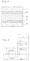
- FIG. 2 there is shown, in a fragmentary sectional representation, a basic structure of a liquid crystal display device adapted to be driven by a drive method according to one embodiment of the present invention.
- the liquid crystal display device shown therein comprises a pair of first and second transparent substrates 1 and 2 positioned one above the other in spaced relationship with each other; a plurality of striped scanning electrodes 3 each in the form of a transparent electrode film and deposited on one surface of the first substrate 1, which confronts the second substrate 2; a plurality of striped signal electrodes 4 each in the form of a transparent electrode film and deposited on one surface of the second substrate 2, which confronts the first substrate 1; and a layer 5 of liquid crystal filled up in a space between the first and second substrates 1 and 2.
- the scanning and signal electrodes 3 and 4 are so patterned on the respective surfaces of the first and second substrates 1 and 2 as to extend perpendicular to each other with a pixel formed at each intersection between the scanning and signal electrodes 3 and 4.
- the liquid crystal layer 5 is prepared from a mixture of a high molecular weight liquid crystal of a kind containing, as a main chain, siloxane and, as a side chain, a radical capable of exhibiting a liquid crystalline property, with a low molecular weight liquid crystal capable of exhibiting a nematic characteristic.
- An example of this mixture includes, for example, a mixture of poly-(4-cyanophenyl-4'-hexyloxbenzoate methylcyloxane with a commercially available material identified by "E63" manufactured and sold by Merc, Japan, Inc.
- the liquid crystal layer 5 of the above described composition can be held in a light transmitting state (with 80% or higher light transmissivity) when an alternating voltage having a frequency (for example, 1 kHz) higher than a predetermined frequency (for example, 100 Hz) and also having an effective voltage (for example, 90 volts) higher than a predetermined voltage (for example, 50 volts) is applied between the scanning and signal electrodes 3 and 4, but can be held in a light scattering state (with 50% or lower light transmissivity) when a high electric voltage having a relatively low frequency (1 Hz to a direct current) and also having an effective voltage higher than the above described predetermined voltage is applied between the scanning and signal electrodes 3 and 4.
- a light transmitting state with 80% or higher light transmissivity
- the liquid crystal layer 5 allows the passage of the incident light therethrough when in the light transmitting state, but scatters the incident light when in the light scattering state.
- a voltage for example, 30 volts
- the liquid crystal layer 5 can retain one of the light transmitting and scattering stages which has been held previously.
- the liquid crystal layer 5 of the above described composition has a memory property. It is to be noted that the specific values of the frequency and the voltage referred to above may vary depending on the composition of the liquid crystal layer 5.
- the liquid crystal layer 5 of the above described composition has a film forming capability and can, therefore, assume a film-like shape when a liquid crystal material is applied on the surface of the first substrate 1 on which the scanning electrodes 3 have already been formed. Since the liquid crystal layer 5 has a self-retentivity, cells of relatively large surface area can readily be manufactured with a cell gap controlled strictly and with no need to spread spacers on the substrate such as required where the liquid crystal material in a liquid form is employed. Also, any adjustment of the cell gap to a submicron order and the use of orientation films used to accomplish a monodomain, such as required during the manufacture of cells utilizing a ferroelectric liquid crystal material, are not required.
- the liquid crystal layer 5 contains a nematic liquid crystal in a liquid form, the local viscosity of the liquid crystal layer is low and the liquid crystal layer can be driven at a voltage lower than that required for driving smectic dynamic scattering type cells utilizing a smectic liquid crystal having a relatively high crystalline property.
- Each of the first and second substrates 1 and 2 may be either a transparent glass plate or a transparent resinous film.
- the use of the transparent resinous film is advantageous in that the liquid crystal display device can be made lightweight and thin in thickness and also in that it makes possible to manufacture a flexible liquid crystal display device.
- the transparent resinous film for each of the first and second substrates 1 and 2 includes films of polyethylene terephthalate, polyethylene naphthalate and polyether sulphone.
- a transparent electrode film forming each of the scanning and signal electrodes 3 and 4 may be a film of either indium-tin oxide (ITO) or tin oxide.
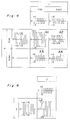
- Fig. 1 illustrates, in a plan representation, the scanning and signal electrodes 3 and 4 used in the liquid crystal display device of the type referred to above.
- Fig. 1 also illustrates waveforms of respective signals Ss and Sd applied to one scanning electrode 3a and one signal electrode 4a and also a waveform of a voltage Sp applied to one pixel P formed at the point of intersection between the scanning and signal electrodes 3a and 4a, for the purpose of a description of the driving method according to the present invention.
- the liquid crystal display device in practice has 50 to 200 scanning electrodes 3 and a corresponding number of the signal electrodes 4. In general, the number of the scanning or signal electrodes employable in practice varies with characteristics of the liquid crystal layer.
- the scanning and signal electrodes 3 and 4 are applied, from an external drive circuit (not shown in Fig. 1) signals of predetermined waveforms corresponding the a content desired to be displayed, so that each of the pixels formed at respective points of intersection between the scanning and signal electrodes 3 and 4 can be driven to assume one of the light transmitting and scattering states thereby to accomplish a display.
- a display operation includes, according to the embodiment of the present invention, an erasing operation, in which an entire display screen is initialized to a light scattering state to erase a display content and a writing operation in which some of the pixels are reversed to assume the light transmitting state, while the remaining pixels are held in the light scattering state, thereby to effect a display of an image desired to be displayed.
- the pixel P to which the scanning signal of the waveform Ss and the signal of the waveform Sd are respectively applied through the scanning electrode 3a and the signal electrode 4a responds to a voltage of the waveform Sp corresponding to a difference between the waveforms Ss and Sd.
- This voltage of the waveform Sp contains a high frequency component of a frequency (for example, 1 kHz) higher than the predetermined frequency (for example, 100 Hz) and a direct current component of a constant voltage.
- periods T31 and T41 during which a direct current voltage is applied to the pixel represent a period during which the entire display is erased and, during such period, the direct current voltage of aE or -aE (wherein a is, for example, 3 and E is, for example, 30 volts) is applied to render the pixel P to assume the light scattering state.
- the application of a sufficiently high direct current voltage causes a turbulent flow in the liquid crystal layer 5 due to movement of ions and, because of this, the rays of light entering the liquid crystal layer 5 are scattered (or clouded white) causing the pixel to assume the light scattering state.
- the direct current voltage applied during the period T31 is reverse in polarity to that of the direct current voltage applied during the period T41.
- any one of periods T33 and T43 during which an alternating current voltage of high effective voltage aE is applied which periods are included respectively within associated periods T32 and T42 during which the high frequency alternating voltage is applied to the pixel P
- liquid crystal molecules forming the liquid crystal layer 5 are oriented homeotropic by the application of the high frequency voltage, thereby causing the pixel P to reverse from the light scattering state to the light transmitting state.
- the alternating voltage of a relatively low effective voltage E which period is included in any one of the periods T32 and T42, the pixel P is retained in the state which has previously been assumed.
- Fig. 3 illustrates waveforms of the signals applied respectively to the scanning and signal electrodes 3a and 4a during the above described erasing operation and a waveform of the voltage applied to the pixel P at the point of intersection between the electrodes 3a and 4a to which the respective signals of the waveforms shown therein have been applied.
- a voltage of the waveform shown in a block at an intersection between the row X and the column Y is applied to the pixel P
- the direct current voltage of a value (a-1)E which does not vary during the erasing period T31, is applied from the scanning electrode 3a and the direct current voltage of a value E and of a polarity reverse to that of the signal applied to the scanning electrode 3a is applied from the signal electrode 4a.
- an erasure of a display during a display of one picture is carried out by the application of a signal shown by the solid line in Fig. 3
- an erasure of a display during a display of the next succeeding picture can be carried out by the application of a signal shown by the phantom line in Fig. 3.
- the scanning and signal electrodes 3a and 4a are applied with respective signals each having a polarity reversed for each picture and, consequently, the pixel P is applied with the direct current voltage aE of a polarity reversed for each picture.
- all of the scanning electrodes 3 are applied equally with the signal of the waveform shown in the row X in Fig. 3 and all of the signal electrodes 4 are applied equally with the signal of the waveform shown in the column Y in Fig. 3. Accordingly, all of the pixels forming a display screen can be simultaneously reversed from the light transmitting state to the light scattering state at a time.
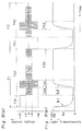
- Fig. 4 illustrates waveforms of the signals applied respectively to the scanning and signal electrodes 3 and 4 during the above described writing operation and waveforms of the voltages applied to the pixels P at the point of intersection between the electrodes 3 and 4 to which the respective signals of the waveforms shown therein have been applied.
- the waveforms in Fig. 4 are depicted in a manner similar to those in Fig. 3 and, thus, it will readily be understood that, when the signals of the waveforms shown in the row X and the column Y are applied respectively to the electrodes 3 and 4, the voltages of the respective waveforms shown at intersection between the row X and the column Y are applied to the pixels at respective points of intersection between the scanning and signal electrodes 3 and 4.
- the plural scanning electrodes 3 are line-sequentially selected and, when selected, each scanning electrode 3 is applied with a scanning signal X ON is applied, but when not selected, each scanning electrode 3 is applied with a scanning signal X OFF .
- the signal electrodes 4 are applied with a signal Y ON during a period in which some of the scanning electrodes 3 corresponding to the pixels desired to be held in the light transmitting state (ON state) on such signal electrodes 4 are selected, but with a signal Y OFF during a period in which some of the scanning electrodes 3 corresponding to the pixels desired to be held in the light scattering state (OFF state) are selected.
- the scanning signal X ON applied to the line sequentially selected scanning electrodes 3 is of a sufficiently high frequency (for example, 1 kHz) and is of a bipolar rectangular wave having an effective voltage (a-1)E (for example, 60 volts when a is 3 and E is 30 volts).
- the scanning signal X OFF applied to some of the scanning electrodes 3 which are not selected is a direct current signal of 0 volt and, hence, no voltage is applied to the non-selected scanning electrodes 3.
- the signal X ON is applied thereto during a period T33 included in the writing period T31 (See Fig. 1) and the signal X OFF is applied thereto during the remaining period included in the writing period T32.
- the signal Y ON applied during the period in which some of the scanning electrodes 3 corresponding to some of the pixels desired to be held in the light transmitting state (ON state) on each of the signal electrodes 4 is of an effective voltage E and is of a bipolar rectangular wave opposite in phase to the scanning signal X ON .
- the signal Y OFF applied during a period in which some of the scanning electrodes 3 corresponding to the pixels desired to be held in the light transmitting state is of an effective voltage E and of a bipolar rectangular wave matched in phase with the scanning signal X ON .
- each of the pixels at respective points of intersection between the scanning and signal electrodes 3 and 4 is applied with a voltage between the scanning electrodes 3 and the signal electrodes 4, some of the pixels at the respective points of intersection between the selected scanning electrode 3 (i.e., some of the scanning electrodes 3 to which the scanning signal X ON is applied) and some of the signal electrodes 4 to which the signal Y ON is applied are applied with a voltage of a waveform shown by A1 in Fig. 4.
- the applied voltage is of a bipolar rectangular wave having the effective voltage aE.
- some of the pixels at the respective points of intersection between the non-selected scanning electrodes 3 i.e., some of the scanning electrodes 3 to which the scanning signal X OFF is applied
- some of the signal electrodes 4 to which the signal Y ON is applied are applied with a voltage of a bipolar rectangular waveform having an effective voltage E as shown by A3 in Fig. 4
- some of the pixels at the respective points of intersection between the non-selected scanning electrodes 3 and some of the signal electrodes 4 to which the signal Y OFF is applied are applied with a voltage of a bipolar rectangular waveform having an effective voltage E as shown by A4 in Fig. 4.
- the alternating voltage of an effective value aE (for example, 90 volts) is applied to the associated pixels at the respective points of intersection between the selected scanning electrodes 3 and the signal electrodes 4 to which the signal Y ON has been applied, or otherwise the alternating voltage of an effective value E or (a-2)E (which may be 30 volts when a is 3) is applied thereto.
- the application of the alternating voltage of the effective value aE results in a change in optical state of the liquid crystal layer 5 and, since when the alternating voltage of the effective value E or (a-2)E is applied the liquid crystal layer 5 retains the previous state which has been assumed before the application of such alternating voltage, only portions of the liquid crystal layer 5 aligned with some of the pixels to which the signals X ON and Y ON have been applied change from the light scattering state (OFF state) to the light transmitting state (ON state). So far as the remaining pixels are concerned, the remaining pixels remain the previous state, that is, in the light scattering state (OFF state) as hereinbefore described.
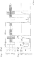
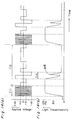
- Fig. 5 is a diagram used to describe a display operation, wherein Fig. 5(a) shows a waveform of the voltage applied to the pixel P shown in Fig. 1 and Fig. 5(b) shows a change in light transmissivity of the pixel P.
- Fig. 5 is applicable where the state of the pixel P is reversed.
- the direct current voltage of a high value aE is applied during the erasing period T31, the light transmissivity abruptly decreases during this period as indicated by b1, rendering the pixel to assume the light scattering state (white clouded state).
- T31 there is no possibility that the light transmissivity may temporarily increase during the course in which the pixel is getting white clouded, because no change occurs in the polarity of the applied voltage.
- the bipolar rectangular wave of the effective voltage E is applied to the pixel P during a period T34 prior to the timing at which the scanning electrode 3a is selected and, during this period, the pixel P is retained in the light scattering state.
- the bipolar rectangular wave of the high effective voltage aE is applied to the pixel P. Accordingly, as indicated by b2 in Fig. 5(b), the light transmissivity of the pixel P increases accompanied by a reversion of the state of the pixel P to the light transmitting state.
- a period T35 following the period T33 represents a period during which the other scanning electrodes 3 are selected and, during this period, the bipolar rectangular wave of the effective voltage E is applied to the associated pixels and, consequently, such pixels are retained in the previously assumed light transmitting state.
- a display of one picture completes during one frame period F1 including the periods T31 and T32 and, during the next succeeding frame period F2 following the period T32, the next succeeding picture can be displayed.
- This next succeeding frame period F2 includes an erasing period T41 and a writing period T42.
- signals of respective waveforms shown by the phantom line in Fig. 3 are applied to the scanning electrode 3a and the signal electrode 4a.
- the signals having respective polarities reversed to those during the period T31 are applied to the scanning electrode 3a and the signal electrode T41 and, consequently, the polarity of the voltage applied to the pixel P is also reversed.
- the direct current voltage Voltage - aE
- the signals having their polarities reversed to those during the writing period T32 for the previous picture display are applied to the scanning and signal electrodes 3a and 4a and, therefore, the alternating voltage having a polarity opposite to that during the period T32 is applied to the pixel P during the writing period T42.
- the waveform of the voltage applied to the pixel P during the period T43 in which the scanning electrode 3a is selected represents a bipolar rectangular waveform having an effective voltage E and, therefore, the state of the pixel P is retained.
- a voltage of a waveform similar to that during any one of the periods T31 and T32 is applied to the pixel P.
- an erasure of a displayed picture by initializing all of the pixels forming the display screen to the light scattering state can be accomplished by applying to the pixels the direct current voltage which does not vary during the entire period in which this erasing operation is carried out. Accordingly, there is no possibility that any temporary increase of the light transmissivity occurs during the erasing period, permitting an efficient change to the light scattering state to take place. Therefore, a display contrast can be increased considerably.
- a successive display of a plurality of consecutive pictures may be said to be accomplished by an alternating current drive and, therefore, any undesirable electrolysis of liquid crystal molecules forming the liquid crystal layer 5 can be advantageously avoided.
- the present invention permits the use of the rectangular waves for the drive signal, a drive circuit can be manufactured simple in structure and low in manufacturing cost.
- the voltage to be applied to the pixels for changing the optical state thereof will be twice to three times the voltage applied to the pixels for maintaining the optical state. Therefore, it is possible to apply a voltage lower than a threshold value required to achieve the change in optical state to some of the pixels whose optical state is desired to be maintained and to apply a higher voltage to some of the pixels whose optical state is desired to be changed, so that the change in optical state can be completed quickly in a short time.
- Figs. 6 and 7 pertains to a second preferred embodiment of the present invention and illustrate various waveforms used to describe the operation of the liquid crystal display device.
- the erasure of the displayed picture is carried out by initializing all of the pixels, forming the display screen, to the light transmitting state and the writing of a display is carried out by reversing the pixels selectively into the light scattering state with respect to the initialized display screen.
- a display substantially reverse to that accomplished according to the foregoing embodiment of the present invention can be accomplished.
- the light transmitting state and the light scattering state are referred to as the OFF state and the ON state, respectively.
- Fig. 6 there is shown the waveforms of signals applied to the scanning and signal electrodes 3 and 4 during the erasing operation, in a manner substantially similar to Fig. 3.
- the scanning electrodes 3 are applied equally with a bipolar rectangular wave of an effective voltage (a-1) having a sufficiently high frequency (for example, 1 kHz) as shown in a row X
- the signal electrodes 4 are applied equally with a bipolar rectangular wave of an effective voltage E and opposite in polarity to that of the signal applied to the scanning electrodes 3, as shown in a column Y.
- all of the pixels forming the display screen can be applied with a bipolar rectangular wave of an effective voltage aE having a sufficiently high frequency as shown at an intersection between the row X and the column Y in Fig. 6 and, accordingly, all of the pixels are held in the light transmitting state (OFF state).
- the waveform of each of the signals may be reversed for each picture and may be either of a type shown in Fig. 6 or of a type reverse to the signal shown in Fig. 6 during a display erasure.
- Fig. 7 illustrates waveforms of signals applied respectively to the scanning and signal electrodes 3 and 4 during the writing operation, in a manner substantially similar to Fig. 4.
- the plural scanning electrodes 3 are line-sequentially selected, and the selected scanning electrodes 3 are applied with a signal X ON which is a direct current voltage having a constant voltage (a-1)E or -(a-1)E over the entire period of selection.
- the non-selected scanning electrodes are applied with a signal X OFF of zero volt which does not vary.
- the signal Y ON is a direct current voltage opposite in polarity to that of the signal X ON and having a voltage -E or E.
- the signal Y OFF is a direct current voltage matched in polarity with that of the signal X ON and having a voltage E or -E.
- each of the pixels to which the signal Y ON is applied from the associated signal electrode 4 is applied with a direct current voltage of a value aE or -aE as shown by B1 so that the pixel can assume the light scattering state (ON state).
- the pixels corresponding to the non-selected electrodes 3 are applied with direct current voltages of respective values E or -E as shown by B3 and B4 and, therefore, the associated pixels retain the previously assumed state.
- Each of the signals X ON , X OFF , Y ON and Y OFF is of a waveform as shown by the solid line in Fig. 7 during a period in which a certain picture is displayed, and is of a waveform as shown by the phantom line in Fig. 7, which is reverse in polarity to the waveform shown by the solid line, during a subsequent period in which the next succeeding picture is displayed.
- Fig. 8 is a diagram used to explain the operation with a particular pixel taken into consideration, wherein Fig. 8(a) illustrates a waveform of the voltage applied to the pixel P at the point of intersection between the scanning and signal electrodes 3a and 4a shown in Fig. 1 during the writing operation, and Fig. 8(b) illustrates a change in light transmissivity.
- a display of one picture is carried out during a single frame period F11 including an erasing period T51 and a writing period T52.
- a bipolar rectangular wave of an effective voltage aE having a high frequency is applied and the light transmissivity therefore increases as indicated by c1 to render the pixel P to assume the light transmitting state (OFF state).
- the waveform of a signal then used is that in which no voltage vary during the selection of one scanning electrode 3 (that is, the cycle of which is twice the length of time during which one scanning electrode is selected).
- the pixel P is applied with a direct current voltage , the voltage aE of which does not vary over the period T53, included in the period T52, in which the scanning electrode 3a is selected. Accordingly, during this period T53, the light transmissivity abruptly decreases as indicated by c2 with no possibility of a temporary increase of the light transmissivity.
- the driving circuit when the pixels are selectively brought into the light scattering state to accomplish a writing of a display content, some of the pixels whose optical states are to be reversed can be applied with the direct current voltage of the non-variable value aE or -aE during the selection of the scanning electrodes corresponding to such pixels and, accordingly, there is no possibility that the light transmissivity may exhibit a temporary increase during the course of change from the light transmitting state to the light scattering state, making it possible to increase the display contrast. Also, since the rectangular wave is used, the driving circuit can be manufactured simple in structure.
- Figs. 9 and 10 pertains to a third preferred embodiment of the present invention and illustrate various waveforms used to describe the operation of the liquid crystal display device. Specifically, Fig. 9 illustrates the waveforms of the signals used during the erasing operation, which waveforms are shown in a fashion substantially similar to those of Fig. 3, and Fig. 10 illustrates the waveforms of the signals used during the writing operation, which waveforms are shown in a fashion substantially similar to those of Fig. 4.
- the waveforms of the signals applied to the scanning and signal electrodes 3 and 4 in the practice of the third embodiment of the present invention are those interchanged with the respective waveforms of the signals applied to the scanning and signal electrodes 3 and 4 used in the first embodiment of the present invention shown in and described with reference to Figs. 1 to 5.
- Even the third embodiment of the present invention can bring about effects similar to those afforded by the first embodiment of the present invention.
- Figs. 11 and 12 pertains to a fourth preferred embodiment of the present invention and illustrate various waveforms used to describe the operation of the liquid crystal display device, wherein Fig. 11 illustrates the waveforms of the signals used during the erasing operation and Fig. 10 illustrates the waveforms of the signals used during the writing operation.
- the waveforms shown in Figs. 11 and 12 are depicted in a fashion substantially similar to those in Figs. 6 and 7, respectively.
- the waveforms of the signals applied to the scanning and signal electrodes 3 and 4 in the practice of the fourth embodiment of the present invention are those interchanged with the respective waveforms of the signals applied to the scanning and signal electrodes 3 and 4 used in the second embodiment of the present invention shown in and described with reference to Figs. 6 to 8. Even the fourth embodiment of the present invention can bring about effects similar to those afforded by the second embodiment of the present invention.
- the present invention may not be always limited to the foregoing embodiments and may be varied in numerous ways.
- the signal to be applied to each of the scanning and signal electrodes 3 and 4 may not be always bipolar, that is, may not be of a polarity varying towards a negative side and also towards a positive side with respect to the zero volt value, and a signal of a waveform obtained by superimposing the signal shown in Figs. 3, 4, 6, 7 and 9 to 12 on the predetermined direct current voltage may be applied to each of the scanning and signal electrodes 3 and 4.
- the liquid crystal layer can be applied with the bipolar rectangular wave.
- the waveform of the signal may not be always limited to a rectangular shape, but may be a sine wave or any other suitable wave provided it can satisfy the required conditions.
- a retaining period may be provided between the erasing and writing periods during which an alternating current voltage of a relatively low effective value or a relatively low direct current voltage is applied to all of the pixels so that each pixel can retain the previously assumed state.
- the mixture of the liquid crystal of a high molecular weight with the liquid crystal of a low molecular weight may be of any suitable kind provided that the state thereof can be changed by a switching of the frequency and that it may have a memory effect by which the adjustment of the applied voltage allows the previously assumed state to be retained for a length of time greater than a predetermined value.
- This driving method includes an erasing operation in which the entire display screen is initialized to render it in either a light transmitting state or a light scattering state, and a writing operation in which the optical state of each of the pixels forming the erased display screen is selectively reversed to accomplish a writing of a display content.
- some of the signal electrodes which correspond to some of the pixels of which optical state is desired to be changed in the selected scanning electrodes are applied with a bipolar rectangular wave of an effective voltage E and having a phase opposite to that of the scanning wave
- some of the signal electrodes which correspond to some of the pixels of which optical state is to be retained are applied with the bipolar rectangular wave of an effective voltage E and having a phase matched with that of the scanning wave.
- the voltage applied to each of the pixels is a difference between the voltage applied to the scanning electrodes and the voltage applied to the signal electrodes.
- the non-selected scanning electrodes both of the pixels corresponding to the signal electrodes to which the signal necessary to change the optical state is applied and the pixels to which the signal necessary to retain the optical state are applied with the bipolar rectangular wave of the effective voltage E (for example, 30 volts).
- the pixels corresponding to the signal electrodes to which the signal of a wave opposite in phase to the scanning wave is applied are applied with the bipolar rectangular wave of the effective voltage aE, causing those pixels to change their optical state.
- a display mode is considered in which the above described erasing operation is accomplished by bringing the entire display screen into the light scattering state and the writing operation is accomplished by reversing the optical state of each of the pixels to the light transmitting state.
- the erasing operation is carried out by, for example, applying to all of the scanning electrodes a wave during the above described selection, that is, a bipolar rectangular wave signal of a low frequency (for example, a direct current to 1 Hz) having an effective voltage (a-1)E, and to all of the signal electrodes a bipolar rectangular wave having an effective voltage E and opposite in phase to the wave applied to the scanning electrodes.
- the writing operation is carried out by the use of a signal of a high frequency (for example, 1 kHz) and having the above described waveform.
- Fig. 13 illustrates a change in voltage applied to the pixel desired to be brought into the light transmitting state and Fig. 13(b) illustrate a change in light transmissivity of such pixel.
- a period T1 represents an erasing period and during this erasing period the bipolar rectangular wave of a low frequency having an effective voltage aE is applied to the pixels. Therefore, the light transmissivity decreases as indicated by a1 in Fig. 13(b).
- a period T2 represents a writing period and during this writing period a rectangular wave of a high frequency is applied to the pixels.
- a period T3 included in the period T2 represents a period during which some of the scanning electrodes corresponding to such pixels are selected and, during this period T3, the bipolar rectangular wave of an effective voltage aE is applied causing the light transmissivity of the pixels to increase as indicated by a2.
- the display mode wherein the erasing operation is accomplished by initializing the entire display screen to bring the latter into the light scattering state and the writing operation is accomplished by reversing the optical state of the pixels selectively to the light transmitting state can be attained by interchanging the frequency used during the erasing operation with that used during the writing operation.
- the operation under this display mode is shown in Fig. 14 wherein Fig. 14(a) illustrates a change in the applied voltage in a fashion similar to Fig. 13(a) and Fig. 14(b) illustrates a change in light transmissivity in a fashion similar to Fig. 13(b).
- a period T11 represents an erasing period
- a period T12 represents a writing period and, during a period T13 included in the period T12, the state of such pixels are reversed to the light scattering state.
- a simple matrix-type liquid crystal display device utilizing the memory effect of the liquid crystal layer made of the mixture of the high molecular weight liquid crystal with the low molecular weight liquid crystal can be realized. Therefore, any increase in number of the pixels will not result in a lowering of the display contrast, making it possible to provide a liquid crystal display device of high resolution.
- the mixture itself has a film forming capability and a self-retentivity, no spread of a spacer for an adjustment of cell gaps is necessary and, therefore, the manufacture is easy to accomplish. Also, as compared with the device wherein a smectic dynamic scattering liquid crystal is employed, a relatively low driving voltage is sufficient.
- the erasure of a displayed content was carried out by applying to all of the pixels a direct current voltage of 90 volts the writing of a display content was carried out by applying an alternating voltage of 90 volts in effective voltage having a frequency of 1 kHz. Also, the displayed picture subsequent to the writing was retained by the application of an alternating voltage of 30 volts in effective voltage.
- the drive of the matrix-type liquid crystal display device can be accomplished by a combination of the erasing operation for erasing the entire display screen and the writing operation for writing an image into the erased display screen and with the use of the liquid crystal layer having a memory effect and utilizing the mixture prepared from the liquid crystal of a high molecular weight and the liquid crystal of a low molecular weight. Accordingly, it is possible to manufacture the inexpensive matrix-type liquid crystal device utilizing the liquid crystal layer having the memory effect.
- the liquid crystal material comprising the mixture of the high molecular weight liquid crystal and the low molecular liquid crystal has a self-retentivity, no spread of a spacer onto a substrate for an adjustment of cell gaps such as required where a liquid crystal material in a liquid form is employed is required, making it possible to provide the matrix-type liquid crystal display device having a relatively large surface area.
- the driving method for the liquid crystal display device of the present invention when during the erasing operation or during the writing operation the optical state of each pixel is desired to be reversed from the light transmitting state to the light scattering state, the direct current voltage which does not vary at least during a period in which the optical state is to be reversed is applied. Accordingly, the polarity of the voltage applied to each pixel during the course of reversion from the light transmitting state to the light scattering state does not vary and, therefore, any undesirable temporary increase of the light transmissivity which is apt to occur during such period can be avoided advantageously. In this way, the erasure or writing of the display content can be accomplished efficiently and, therefore, not only can the display contrast be increased, but the display quality can also be increased.
Landscapes
- Physics & Mathematics (AREA)
- Engineering & Computer Science (AREA)
- Chemical & Material Sciences (AREA)
- Crystallography & Structural Chemistry (AREA)
- General Physics & Mathematics (AREA)
- Computer Hardware Design (AREA)
- Theoretical Computer Science (AREA)
- Nonlinear Science (AREA)
- Mathematical Physics (AREA)
- Optics & Photonics (AREA)
- Liquid Crystal Display Device Control (AREA)
- Liquid Crystal (AREA)
Applications Claiming Priority (4)
| Application Number | Priority Date | Filing Date | Title |
|---|---|---|---|
| JP40391390A JPH04217294A (ja) | 1990-12-19 | 1990-12-19 | 液晶表示装置の駆動方法 |
| JP403913/90 | 1990-12-19 | ||
| JP14536/91 | 1991-02-05 | ||
| JP1453691A JPH04249216A (ja) | 1991-02-05 | 1991-02-05 | 液晶表示装置の駆動方法 |
Publications (3)
| Publication Number | Publication Date |
|---|---|
| EP0491377A2 true EP0491377A2 (de) | 1992-06-24 |
| EP0491377A3 EP0491377A3 (en) | 1992-09-30 |
| EP0491377B1 EP0491377B1 (de) | 1995-05-10 |
Family
ID=26350487
Family Applications (1)
| Application Number | Title | Priority Date | Filing Date |
|---|---|---|---|
| EP91121696A Expired - Lifetime EP0491377B1 (de) | 1990-12-19 | 1991-12-18 | Verfahren zur Steuerung einer Matrix-Flüssigkristallanzeige |
Country Status (6)
| Country | Link |
|---|---|
| US (1) | US5216415A (de) |
| EP (1) | EP0491377B1 (de) |
| KR (1) | KR920012987A (de) |
| CA (1) | CA2057965C (de) |
| DE (1) | DE69109641T2 (de) |
| NO (1) | NO303603B1 (de) |
Cited By (2)
| Publication number | Priority date | Publication date | Assignee | Title |
|---|---|---|---|---|
| US5933203A (en) * | 1997-01-08 | 1999-08-03 | Advanced Display Systems, Inc. | Apparatus for and method of driving a cholesteric liquid crystal flat panel display |
| EP0954841B1 (de) * | 1997-05-07 | 2006-05-17 | Kent State University | Dynamische antriebsverfahren und gerät für eine bistabile flüssigkristallanzeige |
Families Citing this family (19)
| Publication number | Priority date | Publication date | Assignee | Title |
|---|---|---|---|---|
| JP3001317B2 (ja) * | 1992-02-05 | 2000-01-24 | 日本電気株式会社 | アクティブマトリクス型液晶表示装置の駆動方法 |
| JP3712046B2 (ja) * | 2000-05-30 | 2005-11-02 | 富士通株式会社 | 液晶表示装置 |
| JP2002207463A (ja) * | 2000-11-13 | 2002-07-26 | Mitsubishi Electric Corp | 液晶表示装置 |
| US8164557B2 (en) * | 2004-10-29 | 2012-04-24 | Semiconductor Energy Laboratory Co., Ltd. | Liquid crystal display device and method for driving the same |
| TW201021000A (en) * | 2008-11-26 | 2010-06-01 | Ind Tech Res Inst | Driving method and display utilizing the same |
| GB201115898D0 (en) * | 2011-09-14 | 2011-10-26 | Cambridge Entpr Ltd | Optical device |
| GB201115868D0 (en) | 2011-09-14 | 2011-10-26 | Cambridge Entpr Ltd | Driver circuit |
| GB201115899D0 (en) * | 2011-09-14 | 2011-10-26 | Cambridge Entpr Ltd | Optical device |
| US9788772B2 (en) | 2013-01-31 | 2017-10-17 | KHN Solutions, Inc. | Wearable system and method for monitoring intoxication |
| US9192334B2 (en) | 2013-01-31 | 2015-11-24 | KHN Solutions, Inc. | Method and system for monitoring intoxication |
| US8878669B2 (en) | 2013-01-31 | 2014-11-04 | KHN Solutions, Inc. | Method and system for monitoring intoxication |
| US9250228B2 (en) | 2014-01-22 | 2016-02-02 | KHN Solutions, Inc. | Method and system for remotely monitoring intoxication |
| USD727764S1 (en) * | 2014-09-09 | 2015-04-28 | KHN Solutions, Inc. | Breathalyzer |
| USD727763S1 (en) | 2014-09-09 | 2015-04-28 | KHN Solutions, Inc. | Breathalyzer |
| US11324449B2 (en) | 2018-03-22 | 2022-05-10 | KHN Solutions, Inc. | Method and system for transdermal alcohol monitoring |
| US11006895B2 (en) | 2018-03-22 | 2021-05-18 | KHN Solutions, Inc. | Method and system for transdermal alcohol monitoring |
| US12458283B2 (en) | 2021-01-12 | 2025-11-04 | Khn Solutions, Llc | Method and system for remote transdermal alcohol monitoring |
| US11602306B2 (en) | 2021-01-12 | 2023-03-14 | KHN Solutions, Inc. | Method and system for remote transdermal alcohol monitoring |
| US12343133B1 (en) | 2023-10-27 | 2025-07-01 | Khn Solutions, Llc | Method and system for detecting and maintaining performance of an alcohol sensing device |
Family Cites Families (9)
| Publication number | Priority date | Publication date | Assignee | Title |
|---|---|---|---|---|
| US4571585A (en) * | 1983-03-17 | 1986-02-18 | General Electric Company | Matrix addressing of cholesteric liquid crystal display |
| GB2166256B (en) * | 1984-10-25 | 1988-06-08 | Stc Plc | Ferroelectric liquid crystal display cells |
| EP0182509B1 (de) * | 1984-11-14 | 1992-04-08 | Nortel Networks Corporation | Zweidimensionales optisches Informationsverarbeitungsgerät |
| EP0214856B1 (de) * | 1985-09-06 | 1992-07-29 | Matsushita Electric Industrial Co., Ltd. | Verfahren zur Ansteuerung eines Flüssigkristallrasterbildschirmes |
| US4859035A (en) * | 1986-05-26 | 1989-08-22 | Nec Corporation | Ferroelectric liquid crystal light shutter device and method of controlling the driving of the same |
| US4870398A (en) * | 1987-10-08 | 1989-09-26 | Tektronix, Inc. | Drive waveform for ferroelectric displays |
| US4857906A (en) * | 1987-10-08 | 1989-08-15 | Tektronix, Inc. | Complex waveform multiplexer for liquid crystal displays |
| JPH02127494A (ja) * | 1988-11-08 | 1990-05-16 | Chisato Kajiyama | 液晶性組成物 |
| JPH02193115A (ja) * | 1989-01-23 | 1990-07-30 | Chisato Kajiyama | 情報記録媒体 |
-
1991
- 1991-12-13 US US07/806,365 patent/US5216415A/en not_active Expired - Fee Related
- 1991-12-18 CA CA002057965A patent/CA2057965C/en not_active Expired - Fee Related
- 1991-12-18 DE DE69109641T patent/DE69109641T2/de not_active Expired - Fee Related
- 1991-12-18 EP EP91121696A patent/EP0491377B1/de not_active Expired - Lifetime
- 1991-12-18 NO NO915006A patent/NO303603B1/no unknown
- 1991-12-19 KR KR1019910023414A patent/KR920012987A/ko not_active Abandoned
Cited By (2)
| Publication number | Priority date | Publication date | Assignee | Title |
|---|---|---|---|---|
| US5933203A (en) * | 1997-01-08 | 1999-08-03 | Advanced Display Systems, Inc. | Apparatus for and method of driving a cholesteric liquid crystal flat panel display |
| EP0954841B1 (de) * | 1997-05-07 | 2006-05-17 | Kent State University | Dynamische antriebsverfahren und gerät für eine bistabile flüssigkristallanzeige |
Also Published As
| Publication number | Publication date |
|---|---|
| NO915006L (no) | 1992-06-22 |
| DE69109641D1 (de) | 1995-06-14 |
| CA2057965C (en) | 1998-07-07 |
| KR920012987A (ko) | 1992-07-28 |
| EP0491377A3 (en) | 1992-09-30 |
| EP0491377B1 (de) | 1995-05-10 |
| CA2057965A1 (en) | 1992-06-20 |
| NO303603B1 (no) | 1998-08-03 |
| DE69109641T2 (de) | 1995-10-19 |
| NO915006D0 (no) | 1991-12-18 |
| US5216415A (en) | 1993-06-01 |
Similar Documents
| Publication | Publication Date | Title |
|---|---|---|
| EP0491377B1 (de) | Verfahren zur Steuerung einer Matrix-Flüssigkristallanzeige | |
| US5092665A (en) | Driving method for ferroelectric liquid crystal optical modulation device using an auxiliary signal to prevent inversion | |
| KR0167072B1 (ko) | 액정 장치 구동 방법 | |
| EP0197742A2 (de) | Flüssigkristall-Zellenadressierung | |
| EP0240222A1 (de) | Flüssigkristall-Zellenadressierung | |
| JPS6245535B2 (de) | ||
| KR20000069992A (ko) | 초기에는 네마틱 상태로 설정된 콜레스테릭 액정 평판 디스플레이의 구동장치 및 구동방법 | |
| JPS6245536B2 (de) | ||
| JPS6261931B2 (de) | ||
| JPH0629919B2 (ja) | 液晶素子の駆動方法 | |
| US5296953A (en) | Driving method for ferro-electric liquid crystal optical modulation device | |
| JPS6031120A (ja) | 液晶装置 | |
| US5436743A (en) | Method for driving optical modulation device | |
| US4927243A (en) | Method and apparatus for driving optical modulation device | |
| JPS6033535A (ja) | 液晶装置 | |
| CN101647055B (zh) | 具有增强转换装置的液晶显示设备 | |
| JP2502292B2 (ja) | 光学変調素子の駆動法 | |
| JPS62134691A (ja) | 液晶装置 | |
| JPS6256936A (ja) | 液晶マトリツクス表示パネルの駆動法 | |
| JP2614220B2 (ja) | ディスプレイ装置 | |
| JPH04249216A (ja) | 液晶表示装置の駆動方法 | |
| JPS6294829A (ja) | 強誘電性液晶装置 | |
| JPS62133426A (ja) | 液晶装置 | |
| JPH0695179B2 (ja) | 液晶マトリックス表示パネルの駆動法 | |
| JPH0799415B2 (ja) | 液晶装置 |
Legal Events
| Date | Code | Title | Description |
|---|---|---|---|
| PUAI | Public reference made under article 153(3) epc to a published international application that has entered the european phase |
Free format text: ORIGINAL CODE: 0009012 |
|
| AK | Designated contracting states |
Kind code of ref document: A2 Designated state(s): BE DE FR GB IT NL |
|
| PUAL | Search report despatched |
Free format text: ORIGINAL CODE: 0009013 |
|
| AK | Designated contracting states |
Kind code of ref document: A3 Designated state(s): BE DE FR GB IT NL |
|
| 17P | Request for examination filed |
Effective date: 19921211 |
|
| 17Q | First examination report despatched |
Effective date: 19940822 |
|
| GRAA | (expected) grant |
Free format text: ORIGINAL CODE: 0009210 |
|
| AK | Designated contracting states |
Kind code of ref document: B1 Designated state(s): BE DE FR GB IT NL |
|
| REF | Corresponds to: |
Ref document number: 69109641 Country of ref document: DE Date of ref document: 19950614 |
|
| ITF | It: translation for a ep patent filed | ||
| ET | Fr: translation filed | ||
| PLBE | No opposition filed within time limit |
Free format text: ORIGINAL CODE: 0009261 |
|
| STAA | Information on the status of an ep patent application or granted ep patent |
Free format text: STATUS: NO OPPOSITION FILED WITHIN TIME LIMIT |
|
| 26N | No opposition filed | ||
| PGFP | Annual fee paid to national office [announced via postgrant information from national office to epo] |
Ref country code: GB Payment date: 19971209 Year of fee payment: 7 Ref country code: FR Payment date: 19971209 Year of fee payment: 7 |
|
| PGFP | Annual fee paid to national office [announced via postgrant information from national office to epo] |
Ref country code: NL Payment date: 19971223 Year of fee payment: 7 |
|
| PGFP | Annual fee paid to national office [announced via postgrant information from national office to epo] |
Ref country code: DE Payment date: 19971230 Year of fee payment: 7 |
|
| PGFP | Annual fee paid to national office [announced via postgrant information from national office to epo] |
Ref country code: BE Payment date: 19980217 Year of fee payment: 7 |
|
| PG25 | Lapsed in a contracting state [announced via postgrant information from national office to epo] |
Ref country code: GB Free format text: LAPSE BECAUSE OF NON-PAYMENT OF DUE FEES Effective date: 19981218 |
|
| PG25 | Lapsed in a contracting state [announced via postgrant information from national office to epo] |
Ref country code: BE Free format text: LAPSE BECAUSE OF NON-PAYMENT OF DUE FEES Effective date: 19981231 |
|
| BERE | Be: lapsed |
Owner name: SUMITOMO ELECTRIC INDUSTRIES LTD Effective date: 19981231 |
|
| PG25 | Lapsed in a contracting state [announced via postgrant information from national office to epo] |
Ref country code: NL Free format text: LAPSE BECAUSE OF NON-PAYMENT OF DUE FEES Effective date: 19990701 |
|
| GBPC | Gb: european patent ceased through non-payment of renewal fee |
Effective date: 19981218 |
|
| PG25 | Lapsed in a contracting state [announced via postgrant information from national office to epo] |
Ref country code: FR Free format text: LAPSE BECAUSE OF NON-PAYMENT OF DUE FEES Effective date: 19990831 |
|
| NLV4 | Nl: lapsed or anulled due to non-payment of the annual fee |
Effective date: 19990701 |
|
| REG | Reference to a national code |
Ref country code: FR Ref legal event code: ST |
|
| PG25 | Lapsed in a contracting state [announced via postgrant information from national office to epo] |
Ref country code: DE Free format text: LAPSE BECAUSE OF NON-PAYMENT OF DUE FEES Effective date: 19991001 |
|
| PG25 | Lapsed in a contracting state [announced via postgrant information from national office to epo] |
Ref country code: IT Free format text: LAPSE BECAUSE OF NON-PAYMENT OF DUE FEES;WARNING: LAPSES OF ITALIAN PATENTS WITH EFFECTIVE DATE BEFORE 2007 MAY HAVE OCCURRED AT ANY TIME BEFORE 2007. THE CORRECT EFFECTIVE DATE MAY BE DIFFERENT FROM THE ONE RECORDED. Effective date: 20051218 |