EP0491433A2 - Méthode de formation d'une region conductrice dans matériau semi-conducteur en silicium, et dispositif semi-conducteur en silicium avec telle region - Google Patents
Méthode de formation d'une region conductrice dans matériau semi-conducteur en silicium, et dispositif semi-conducteur en silicium avec telle region Download PDFInfo
- Publication number
- EP0491433A2 EP0491433A2 EP91203261A EP91203261A EP0491433A2 EP 0491433 A2 EP0491433 A2 EP 0491433A2 EP 91203261 A EP91203261 A EP 91203261A EP 91203261 A EP91203261 A EP 91203261A EP 0491433 A2 EP0491433 A2 EP 0491433A2
- Authority
- EP
- European Patent Office
- Prior art keywords
- layer
- tungsten
- silicide
- formation
- molybdenum
- Prior art date
- Legal status (The legal status is an assumption and is not a legal conclusion. Google has not performed a legal analysis and makes no representation as to the accuracy of the status listed.)
- Ceased
Links
Images

Classifications
-
- H—ELECTRICITY
- H10—SEMICONDUCTOR DEVICES; ELECTRIC SOLID-STATE DEVICES NOT OTHERWISE PROVIDED FOR
- H10W—GENERIC PACKAGES, INTERCONNECTIONS, CONNECTORS OR OTHER CONSTRUCTIONAL DETAILS OF DEVICES COVERED BY CLASS H10
- H10W20/00—Interconnections in chips, wafers or substrates
- H10W20/40—Interconnections external to wafers or substrates, e.g. back-end-of-line [BEOL] metallisations or vias connecting to gate electrodes
- H10W20/41—Interconnections external to wafers or substrates, e.g. back-end-of-line [BEOL] metallisations or vias connecting to gate electrodes characterised by their conductive parts
- H10W20/425—Barrier, adhesion or liner layers
-
- H—ELECTRICITY
- H10—SEMICONDUCTOR DEVICES; ELECTRIC SOLID-STATE DEVICES NOT OTHERWISE PROVIDED FOR
- H10D—INORGANIC ELECTRIC SEMICONDUCTOR DEVICES
- H10D64/00—Electrodes of devices having potential barriers
- H10D64/01—Manufacture or treatment
- H10D64/011—Manufacture or treatment of electrodes ohmically coupled to a semiconductor
- H10D64/0111—Manufacture or treatment of electrodes ohmically coupled to a semiconductor to Group IV semiconductors
- H10D64/0112—Manufacture or treatment of electrodes ohmically coupled to a semiconductor to Group IV semiconductors using conductive layers comprising silicides
-
- H—ELECTRICITY
- H10—SEMICONDUCTOR DEVICES; ELECTRIC SOLID-STATE DEVICES NOT OTHERWISE PROVIDED FOR
- H10W—GENERIC PACKAGES, INTERCONNECTIONS, CONNECTORS OR OTHER CONSTRUCTIONAL DETAILS OF DEVICES COVERED BY CLASS H10
- H10W20/00—Interconnections in chips, wafers or substrates
- H10W20/40—Interconnections external to wafers or substrates, e.g. back-end-of-line [BEOL] metallisations or vias connecting to gate electrodes
Definitions
- the invention relates to a method of manufacturing a semiconductor device having a conductive region on silicon semiconductor material, more particularly a contact with the semiconductor material.
- silicon semiconductor material and “silicon” refer to monocrystalline silicon as well as to non-monocrystalline (e.g., amorphous or polycrystalline) silicon.
- noble metal silicides e.g., the silicides of titanium (Ti) and cobalt (Co) have been used to form contacts to a semiconductor region where a diffusion or an implantation has been previously done, and to polysilicon to provide low contact resistance or highly conductive interconnects. Titanium and cobalt are preferred because they offer low contact resistance with silicon.
- the electrical resistance of titanium silicide and of cobalt silicide are the lowest among noble- and refractory-metal silicides.
- their silicides can be formed on silicon in a self-aligned manner. That is, these silicides can be formed at locations having predetermined chemical properties, thus rendering the use of an additional mask superfluous.
- titanium silicide will be formed upon deposition of titanium on silicon even in the presence of an oxide layer over the silicon up to a thickness of approximately 40 angstroms, thereby avoiding the need for a separate oxide removal step, e.g. sputter-etch.
- tungsten (W) and molybdenum (Mo) have received much attention as well because of their low electrical resistivities and favorable characteristics with regard to use as contact opening or via opening fills.
- the use of chemical vapor deposition (CVD) of tungsten for fabricating inter-connections provides good step coverage.
- tungsten and molybdenum, selectively deposited through the CVD process can be used as a diffusion barrier, as a polysilicon shunt to reduce interconnection resistance, and as an interconnection in multi-level metallization.
- a blanket CVD-tungsten process is reported, a major aspect whereof relates to the adhesion of CVD-tungsten to silicon oxide.
- the effect upon contact resistance to titanium silicide of this tungsten deposition process in combination with several adhesion layers to oxide is described.
- One of the combinations mentioned includes a tungsten silicide adhesion layer between titanium silicide and a CVD-tungsten blanket.
- This tungsten silicide layer is formed by means of a CVD process using a mixture of silane (SiH4), tungsten hexafluoride and hydrogen, the silane being provided for growth rate enhancement. It was reported that the silane chemistry is effective in reducing fluorine incorporation in the underlying titanium layer. However, this blanket deposition approach appeared to be rather unsuccessful in that it did not provide adhesion at the one-micron diameter contact level.
- a method according to the invention therefore comprises the following steps:
- the materials are to be chosen such as to comply with the following requirements: the layers should provide an adequately conductive coupling with the silicon; each layer should act as an adequate adhesion layer for the succeeding layer; neither the materials used in a particular step nor the formation itself of the associated layer should detrimentally interfere with the conductive characteristics of the preceding layer.
- the use of CVD-tungsten or CVD-molybdenum in the formation of the third layer preferably entails fluorine chemistry.
- the second silicide layer should therefore protect the first silicide layer from being degraded by fluorine compounds while offering good adhesion to both the underlying first layer and the overlying CVD-tungsten layer.
- the materials used preferably have such properties that the formation of the conductive region is established in a self-aligned manner.
- Particular embodiments of a method according to the invention are those wherein the formation of the first layer involves deposition of at least one of the following materials: titanium and cobalt; wherein the formation of the second layer includes physical vapor deposition of at least one of the following: molybdenum and tungsten; and wherein the formation of the third layer includes chemical vapor deposition of at least one of the following: tungsten and molybdenum.
- the physical vapor deposition, such as sputtering or vacuum evaporation, of molybdenum or tungsten is compatible with the CVD-tungsten step and CVD-molybdenum step since the associated silicide generated during subsequent annealing will function as a nucleation layer.
- sputtered tungsten is favored.
- the blanket CVD-tungsten process in Ellwanger employs a CVD-tungsten-silicide step for forming an adhesion promoting layer to oxide with the help of silane that functions, among others, as some sort of a palliative for reducing fluorine damage to the underlying titanium silicide layer.
- a method according to the invention avoids right from the start the use of any substance in the formation of the second layer that may have damaging effects on the first layer.
- Ellwanger uses a blanket CVD-tungsten process wherein the adhesion of the tungsten blanket to the oxide or other dielectric material represents an important criterion for the selection of the various materials and process parameters.
- the CVD-process is of the selective type wherein the deposition of the metal does not occur on dielectric material. This selective type process involves globally different layer materials and process parameters.
- Ellwanger reports loss of adhesion at the one-micron diameter contact level and attributes this to the adhesion properties of the tungsten silicide that was grown in his CVD-tungsten process, whereas in an embodiment according to the invention the second layer is created through a physical deposition of tungsten followed by an anneal step.
- Figs. 1 to 7 show a sequence of steps in a method according to the invention.
- like reference numerals indicate identical or corresponding features.
- Fig. 1 shows by way of example a cross-section of a part of a silicon semiconductor P-type substrate 10 that includes N-doped regions 12 and 14 that will become the source region and the drain region of an N-channel field effect transistor, an annular thermally grown oxide region 16, a dielectric layer 20 electrically isolating substrate 10 from a polysilicon portion 22 that will become the gate of the transistor, and oxide sidewall spacers 24 and 26.
- the feature dimensions are on the order of 1 micron or less.
- a layer of titanium is deposited on top of the structure in Fig. 1, preferably in an argon environment by means of sputtering or vacuum evaporation. Other ways of depositing titanium may include CVD. The thickness of this layer is typically in the range of 100 - 1000 angstroms.
- a rapid (1 to 120 sec.) thermal anneal step in a nitrogen-containing environment at a temperature of 600°C - 700°C is performed. The rapid thermal anneal causes the titanium overlying the silicon to form a lower layer of high-resistive titanium silicide and an upper layer of a titanium-nitrogen-oxygen compound, whereas the titanium overlying the oxide does not react with the oxide. The titanium overlying the oxide forms only a titanium-nitrogen-oxygen compound.
- a conventional anneal step may be carried out in a nitrogen-containing environment at a temperature between 500°C - 700°C for about 15 minutes to 1 hour.
- a selective strip of the titanium-nitrogen-oxygen compound leaves behind self-aligned areas of high-resistivity titanium silicide overlying the silicon.
- a second thermal anneal step is performed in, for instance, a nitrogen-containing or an argon-containing, oxygen-free environment at a temperature of about 700°C - 900°C to transform the high-resistivity titanium silicide into low-resistive titanium silicide. The result is shown in Fig. 2, wherein low-resistivity titanium silicide layers 28, 30 and 32 respectively cover the silicon areas 12, 14 and 22.
- an electrically insulating layer for example, a silicon oxide layer, a phosphosilicate glass layer (PSG), a borosilicate glass layer (BSG), a boron-doped phosphosilicate glass layer (BPSG), a plasma oxide layer or a plasma silicon nitride layer, is formed over the substrate.
- the thickness of this dielectric layer is typically 3000 - 10000 angstroms. If necessary, the dielectric layer may be planarized with various techniques. In case of a PSG-, a BSG- or a BPSG-layer a thermal anneal may be employed to flow and thus planarize the glass.
- Other tecniques include photoresist etchback planarization, spin-on glass (SOG) planarization and planarization by mechanical polishing.
- contact openings are formed by means of etching, typically using photoresist as mask. Thereafter the substrate is covered with a layer of tungsten, for instance by means of sputtering. Typically, the thickness of the tungsten layer is 100 - 1000 angstrom. It should be noted that titanium silicide etches very fast in hydrogen fluoride-based solutions usually used before metal deposition thereon. Therefore the conventional dip in the diluted HF solution should not be done. Instead, a sputter etch step may be performed prior to molybdenum deposition if necessary. In Fig. 3 oxide layer 34 and the titanium silicide layers 28, 30 and 32 at the bottom of the contact holes are covered by tungsten layer 36.
- tungsten silicide formation is accomplished by thermal anneal, resulting in tungsten silicide layers on top of titanium silicide layers 28, 30 and 32, and an unreacted tungsten layer over oxide layer 34.
- the tungsten silicide formation from silicon and tungsten is facilitated by the interposed titanium silicide.
- the reason for this is that the direct formation of tungsten silicide at the tungsten/silicon interface can be retarded by the presence of a thin silicon oxide layer. The thin silicon oxide is readily reduced due to the titanium.
- the presence of titanium silicide also reduces the thermal energy that is necessary for removing silicon from the silicon substrate to form tungsten silicide.
- the temperature at which tungsten silicide forms during annealing should lie approximately between 600°C and 900°C. At a temperature substantially lower than 600°C no tungsten silicide formation occurs, whereas at a temperature higher than 900°C intermixing of silicon, titanium and tungsten and intermixing of tungsten and oxide develops.
- the tungsten that overlays oxide layer 34 is selectively removed, for instance, by means of a selective etching solution. The result is shown in Fig. 4, wherein tungsten silicide layers 37, 38 and 40 respectively cover titanium silicide layers 28, 30 and 32.
- a selective CVD of tungsten is carried out causing a growth of tungsten on top of tungsten silicide layers 37, 38 and 40.
- the CVD tungsten uses tungsten hexafluoride/hydrogen or tungsten hexafluoride/argon as a source gas.
- the deposition temperature preferably lies in the range of 200°C - 700°C
- the deposition pressure lies substantially between 0.01 torr and 100 torr
- the deposition time ranges from substantially 1 minute to 4 hours.
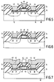
- Fig. 5 The result of the tungsten filling of the contact holes is shown in Fig. 5, wherein layers of tungsten 42, 44 and 46 are deposited on top of the tungsten silicide layers 37, 38 and 40, respectively.
- the contact hole to the polysilicon 22 is shallower than the contact holes to the doped regions 12 and 14.
- the tungsten layer 46 has an outgrown part overtopping oxide layer 34. This part may be removed by a conventional resist etchback approach if the difference in height is unacceptable for some reason.
- the result after the resist etchback is shown in Fig. 6.
- Fig. 7 shows for the sake of completeness parts of interconnects 48, 50 and 52 contacting respectively the tungsten layers 42, 44 and 46.
- the interconnects 48, 50 and 52 are formed, for instance, by depositing aluminum or an aluminum alloy.
- the major alloying materials include silicon, copper, titanium and tungsten.
- the interconnects may also be formed by using other wellconducting materials, such as copper or gold.
- a prominent feature of the above example is that the titanium silicide, the tungsten silicide and the selective tungsten fill through the CVD process all are formed in a self-aligned manner. Furthermore, the titanium silicide that was formed in a self-aligned way, serves a major function of lowering the resistances of monocrystalline silicon and polycrystalline silicon interconnects. As already mentioned, the titanium silicide also reduces the contact resistance.
- molybdenum silicide instead of tungsten silicide in the second layer, physically deposited molybdenum may be used for the formation of the second layer.
- the anneal temperature for the formation of molybdenum silicide should lie between 500°C and 800°C. Below 500°C no silicide is formed, whereas above 800°C undesired intermixing of silicon, titanium or cobalt, and molybdenum occurs.
- a CVD step involving molybdenum may be used with molybdenum hexafluoride/hydrogen or molybdenum hexafluoride/argon as a source gas.
- the deposition temperature should lie substantially between 200°C and 500°C.
- the deposition time typically lies on the order of 5 minutes - 1 hour.
- the deposition pressure lies in the typical range of 0.1 - 10 torr.
- the sequence of steps may be altered. Initially, the first layer was formed over the silicon, a dielectric layer with contact openings was formed over the first layer, the second layer was formed and finally the third layer was formed. Alternatives for the above example are given below.
- a first alternative incorporates forming a dielectric layer with contact openings over the silicon, performing a physical vapor deposition of the first conductive material, executing a first thermal anneal, performing a selective strip of the non-silicided portion of the conductive material, executing a physical vapor deposition of the second conductive material, executing a second thermal anneal, performing a selective strip of the non-silicided portion of the second material and finally carrying out a chemical vapor deposition of the third conductive material.
- This first alternative may apply when the resistance of the silicides is not critical, for example, in interconnects. The interconnect's overall resistance is determined by the third conductive material in a parallel arrangement with the first and the second layers. Consequently, the additional anneal step for further reducing the resistivity of the relevant silicide, as mentioned in the illustrated example, may be left out.
- the anneal steps required for the formation of the first and second layers may be combined into a single anneal step after deposition of the first and second conductive materials at a temperature that enables the relevant silicides to be formed and avoids the intermixing as mentioned above. Subsequently, the selective strip of the non-silicided portion of the second conductive material precedes the selective strip of the non-silicided portion of the first conductive material. Finally, the third conductive material is deposited.
- a third alternative includes a physical vapor deposition of the first conductive material on the substrate, after which a first thermal anneal and a selective strip of the non-silicided portion of the conductive material are carried out. Thereupon the second conductive material is deposited followed by a second anneal step and a selective strip of the non-silicided portion of this material. Thereafter the third conductive material is deposited followed by the formation of a dielectric layer having contact openings that are again filled by the third conductive material.
- the required anneal steps for forming the first and second layers may be combined into a single one.
- a fifth alternative includes a physical vapor deposition of the first conductive material on the substrate followed by a first thermal anneal, a physical vapor deposition of the second conductive material, and a second thermal anneal.
- a dielectric layer is then formed with contact holes that are filled by means of a chemical vapor deposition of the third conductive material.
- the thermal anneal steps may again be replaced by a single one after depositing the first and second conductive materials.
- the above scenarios have been presented by way of example as related to the formation of a (vertical) contact, they also apply to the formation of a horizontal interconnect.
- the scheme given in the figures may be simplified by dispensing with the second thermal anneal of the titanium silicide for the transformation into a low-resistive silicide.
- the interconnect formed by a layered structure according to the invention electrically constitutes a parallel arrangement of three resistances of which the lowest value is represented by the third layer and of which the highest value is represented by the first or the second layer.
- the additional anneal step for the first layer would not contribute significantly to a decrease in the aggregated resistance.
- the additional advantage of the third and fourth alternatives using tungsten or molybdenum in the third layer is that these materials function as an etchstop when local interconnects or straps are used in circuits.
- the method according to the invention is not limited to self-alignedness. Also, though the figures show an example with regard to the realization of a field effect transistor, the method according to the invention extends to the formation of contact hole fills for all kinds of silicon semiconductor devices.
Landscapes
- Internal Circuitry In Semiconductor Integrated Circuit Devices (AREA)
- Electrodes Of Semiconductors (AREA)
- Insulated Gate Type Field-Effect Transistor (AREA)
Applications Claiming Priority (2)
| Application Number | Priority Date | Filing Date | Title |
|---|---|---|---|
| US63010590A | 1990-12-19 | 1990-12-19 | |
| US630105 | 1990-12-19 |
Publications (2)
| Publication Number | Publication Date |
|---|---|
| EP0491433A2 true EP0491433A2 (fr) | 1992-06-24 |
| EP0491433A3 EP0491433A3 (en) | 1992-09-02 |
Family
ID=24525788
Family Applications (1)
| Application Number | Title | Priority Date | Filing Date |
|---|---|---|---|
| EP19910203261 Ceased EP0491433A3 (en) | 1990-12-19 | 1991-12-12 | Method of forming conductive region on silicon semiconductor material, and silicon semiconductor device with such region |
Country Status (3)
| Country | Link |
|---|---|
| US (1) | US5646070A (fr) |
| EP (1) | EP0491433A3 (fr) |
| JP (1) | JP2685679B2 (fr) |
Cited By (2)
| Publication number | Priority date | Publication date | Assignee | Title |
|---|---|---|---|---|
| FR2702089A1 (fr) * | 1993-02-25 | 1994-09-02 | Mitsubishi Electric Corp | Transistor à effet de champ et procédé pour sa production. |
| EP0725431A3 (fr) * | 1995-01-31 | 1999-10-27 | Advanced Micro Devices, Inc. | Méthode de formation d'une structure ordonnée de nitrure de titane et de siliciure de titane sur un substrat semiconducteur, par l'utilisation d'un recuit en trois étapes |
Families Citing this family (15)
| Publication number | Priority date | Publication date | Assignee | Title |
|---|---|---|---|---|
| JP2751859B2 (ja) * | 1995-03-15 | 1998-05-18 | 日本電気株式会社 | 半導体装置の製造方法 |
| US7701059B1 (en) * | 1997-08-21 | 2010-04-20 | Micron Technology, Inc. | Low resistance metal silicide local interconnects and a method of making |
| US6255150B1 (en) * | 1997-10-23 | 2001-07-03 | Texas Instruments Incorporated | Use of crystalline SiOx barriers for Si-based resonant tunneling diodes |
| KR100257075B1 (ko) * | 1998-01-13 | 2000-05-15 | 김영환 | 반도체 소자 및 그의 제조방법 |
| US6303504B1 (en) | 1998-02-26 | 2001-10-16 | Vlsi Technology, Inc. | Method of improving process robustness of nickel salicide in semiconductors |
| US6156649A (en) * | 1998-04-14 | 2000-12-05 | Advanced Micro Devices, Inc. | Method of forming uniform sheet resistivity salicide |
| US6110811A (en) * | 1998-06-11 | 2000-08-29 | Chartered Semiconductor Manufacturing Ltd. | Selective CVD TiSi2 deposition with TiSi2 liner |
| TW502337B (en) | 2001-04-20 | 2002-09-11 | Promos Technologies Inc | Method for reducing WSix grain and its structure |
| US6969678B1 (en) * | 2003-11-03 | 2005-11-29 | Advanced Micro Devices, Inc. | Multi-silicide in integrated circuit technology |
| KR100550345B1 (ko) * | 2004-10-11 | 2006-02-08 | 삼성전자주식회사 | 반도체 장치의 실리사이드막 형성방법 |
| US7229920B2 (en) * | 2005-01-11 | 2007-06-12 | United Microelectronics Corp. | Method of fabricating metal silicide layer |
| US7985668B1 (en) * | 2010-11-17 | 2011-07-26 | Globalfoundries Inc. | Method for forming a metal silicide having a lower potential for containing material defects |
| US8652914B2 (en) | 2011-03-03 | 2014-02-18 | International Business Machines Corporation | Two-step silicide formation |
| RU2610055C1 (ru) * | 2015-11-30 | 2017-02-07 | Федеральное государственное бюджетное образовательное учреждение высшего образования Чеченский государственный университет (ФГБОУ ВО Чеченский государственный университет) | Способ изготовления полупроводникового прибора |
| CN115966549B (zh) * | 2021-10-08 | 2025-12-19 | 中芯国际集成电路制造(上海)有限公司 | 电阻结构及其形成方法 |
Family Cites Families (20)
| Publication number | Priority date | Publication date | Assignee | Title |
|---|---|---|---|---|
| JPS60130825A (ja) * | 1983-12-19 | 1985-07-12 | Toshiba Corp | 半導体装置の製造方法 |
| JPS61166075A (ja) * | 1985-01-17 | 1986-07-26 | Mitsubishi Electric Corp | 半導体装置およびその製造方法 |
| JPS61296764A (ja) * | 1985-06-25 | 1986-12-27 | Mitsubishi Electric Corp | 金属電極配線膜を有する半導体装置 |
| US4818723A (en) * | 1985-11-27 | 1989-04-04 | Advanced Micro Devices, Inc. | Silicide contact plug formation technique |
| JPS6358943A (ja) * | 1986-08-29 | 1988-03-14 | Mitsubishi Electric Corp | 電極・配線膜の構造 |
| US4966865A (en) * | 1987-02-05 | 1990-10-30 | Texas Instruments Incorporated | Method for planarization of a semiconductor device prior to metallization |
| JPH0666456B2 (ja) * | 1987-08-27 | 1994-08-24 | 日本電気株式会社 | コンタクト接続構造 |
| JPS6459954A (en) * | 1987-08-31 | 1989-03-07 | Nec Corp | Semiconductor integrated circuit |
| FR2624304B1 (fr) * | 1987-12-04 | 1990-05-04 | Philips Nv | Procede pour etablir une structure d'interconnexion electrique sur un dispositif semiconducteur au silicium |
| JP2582596B2 (ja) * | 1987-12-17 | 1997-02-19 | 富士通株式会社 | 半導体装置の製造方法 |
| NL8800221A (nl) * | 1988-01-29 | 1989-08-16 | Philips Nv | Werkwijze voor het vervaardigen van een halfgeleiderinrichting. |
| EP0704883A3 (fr) * | 1988-02-11 | 1997-07-09 | Sgs Thomson Microelectronics | Chapeau de siliciure de métal réfractaire, pour protéger les structures multicouches de polycide |
| JPH01286447A (ja) * | 1988-05-13 | 1989-11-17 | Mitsubishi Electric Corp | 半導体装置及びその製造方法 |
| JPH01298765A (ja) * | 1988-05-27 | 1989-12-01 | Fujitsu Ltd | 半導体装置及びその製造方法 |
| JPH01321656A (ja) * | 1988-06-23 | 1989-12-27 | Fujitsu Ltd | 半導体装置 |
| JPH0756866B2 (ja) * | 1988-10-17 | 1995-06-14 | 日本電気株式会社 | 半導体集積回路装置の製造方法 |
| US4954214A (en) * | 1989-01-05 | 1990-09-04 | Northern Telecom Limited | Method for making interconnect structures for VLSI devices |
| JP2543192B2 (ja) * | 1989-07-10 | 1996-10-16 | 松下電器産業株式会社 | 半導体装置およびその製造方法 |
| US5094981A (en) * | 1990-04-17 | 1992-03-10 | North American Philips Corporation, Signetics Div. | Technique for manufacturing interconnections for a semiconductor device by annealing layers of titanium and a barrier material above 550° C. |
| US5023201A (en) * | 1990-08-30 | 1991-06-11 | Cornell Research Foundation, Inc. | Selective deposition of tungsten on TiSi2 |
-
1991
- 1991-12-12 EP EP19910203261 patent/EP0491433A3/en not_active Ceased
- 1991-12-16 JP JP3331020A patent/JP2685679B2/ja not_active Expired - Lifetime
-
1995
- 1995-03-06 US US08/400,778 patent/US5646070A/en not_active Expired - Fee Related
Cited By (2)
| Publication number | Priority date | Publication date | Assignee | Title |
|---|---|---|---|---|
| FR2702089A1 (fr) * | 1993-02-25 | 1994-09-02 | Mitsubishi Electric Corp | Transistor à effet de champ et procédé pour sa production. |
| EP0725431A3 (fr) * | 1995-01-31 | 1999-10-27 | Advanced Micro Devices, Inc. | Méthode de formation d'une structure ordonnée de nitrure de titane et de siliciure de titane sur un substrat semiconducteur, par l'utilisation d'un recuit en trois étapes |
Also Published As
| Publication number | Publication date |
|---|---|
| JP2685679B2 (ja) | 1997-12-03 |
| EP0491433A3 (en) | 1992-09-02 |
| JPH05152450A (ja) | 1993-06-18 |
| US5646070A (en) | 1997-07-08 |
Similar Documents
| Publication | Publication Date | Title |
|---|---|---|
| EP3738143B1 (fr) | Structures d'interconnexion métalliques à faible résistivité avec couches barrières de diffusion à auto-formation | |
| US5614437A (en) | Method for fabricating reliable metallization with Ta-Si-N barrier for semiconductors | |
| US6028000A (en) | Method of forming contact plugs in semiconductor device having different sized contact holes | |
| EP0279588B1 (fr) | Contact dans une perforation dans un semi-conducteur et procédé pour sa fabrication | |
| EP0506426B1 (fr) | Métallisation d'un circuit intégré satisfaisant les exigences d'un coffret à contact zéro et la méthode pour sa préparation | |
| US5646070A (en) | Method of forming conductive region on silicon semiconductor material, and silicon semiconductor device with such region | |
| US5063175A (en) | Method for manufacturing a planar electrical interconnection utilizing isotropic deposition of conductive material | |
| US7051934B2 (en) | Methods of forming metal layers in integrated circuit devices using selective deposition on edges of recesses | |
| US4960732A (en) | Contact plug and interconnect employing a barrier lining and a backfilled conductor material | |
| US5869901A (en) | Semiconductor device having aluminum interconnection and method of manufacturing the same | |
| JP3049487B2 (ja) | 金属配線構造及びその形成方法 | |
| US6955979B2 (en) | Methods for making metallization structures for semiconductor device interconnects | |
| US10170423B2 (en) | Metal cap integration by local alloying | |
| US5846881A (en) | Low cost DRAM metallization | |
| US7790611B2 (en) | Method for FEOL and BEOL wiring | |
| US6617689B1 (en) | Metal line and method of suppressing void formation therein | |
| US20020197857A1 (en) | Method of using tantalum-aluminum-nitrogen material as diffusion barrier and adhesion layer in semiconductor devices | |
| JP3102405B2 (ja) | 半導体装置の製造方法 | |
| US10832947B2 (en) | Fully aligned via formation without metal recessing | |
| US6326306B1 (en) | Method of forming copper dual damascene structure | |
| KR20240042464A (ko) | 망간 및 그래핀을 사용하는 금속 배선을 위한 배리어 구성 | |
| JPH0831932A (ja) | 半導体集積回路装置の製造方法 | |
| US6239015B1 (en) | Semiconductor device having polysilicon interconnections and method of making same | |
| US12057395B2 (en) | Top via interconnects without barrier metal between via and above line | |
| US6228735B1 (en) | Method of fabricating thin-film transistor |
Legal Events
| Date | Code | Title | Description |
|---|---|---|---|
| PUAI | Public reference made under article 153(3) epc to a published international application that has entered the european phase |
Free format text: ORIGINAL CODE: 0009012 |
|
| AK | Designated contracting states |
Kind code of ref document: A2 Designated state(s): DE FR GB IT NL |
|
| PUAL | Search report despatched |
Free format text: ORIGINAL CODE: 0009013 |
|
| AK | Designated contracting states |
Kind code of ref document: A3 Designated state(s): DE FR GB IT NL |
|
| 17P | Request for examination filed |
Effective date: 19930223 |
|
| 17Q | First examination report despatched |
Effective date: 19941014 |
|
| STAA | Information on the status of an ep patent application or granted ep patent |
Free format text: STATUS: THE APPLICATION HAS BEEN REFUSED |
|
| 18R | Application refused |
Effective date: 19951105 |