EP0493834A2 - Circuit générateur d'adresses - Google Patents
Circuit générateur d'adresses Download PDFInfo
- Publication number
- EP0493834A2 EP0493834A2 EP91122380A EP91122380A EP0493834A2 EP 0493834 A2 EP0493834 A2 EP 0493834A2 EP 91122380 A EP91122380 A EP 91122380A EP 91122380 A EP91122380 A EP 91122380A EP 0493834 A2 EP0493834 A2 EP 0493834A2
- Authority
- EP
- European Patent Office
- Prior art keywords
- adder
- address
- output
- subtracter
- inputs
- Prior art date
- Legal status (The legal status is an assumption and is not a legal conclusion. Google has not performed a legal analysis and makes no representation as to the accuracy of the status listed.)
- Granted
Links
Images



Classifications
-
- G—PHYSICS
- G06—COMPUTING OR CALCULATING; COUNTING
- G06F—ELECTRIC DIGITAL DATA PROCESSING
- G06F9/00—Arrangements for program control, e.g. control units
- G06F9/06—Arrangements for program control, e.g. control units using stored programs, i.e. using an internal store of processing equipment to receive or retain programs
- G06F9/30—Arrangements for executing machine instructions, e.g. instruction decode
- G06F9/34—Addressing or accessing the instruction operand or the result ; Formation of operand address; Addressing modes
- G06F9/342—Extension of operand address space
-
- G—PHYSICS
- G06—COMPUTING OR CALCULATING; COUNTING
- G06F—ELECTRIC DIGITAL DATA PROCESSING
- G06F1/00—Details not covered by groups G06F3/00 - G06F13/00 and G06F21/00
- G06F1/02—Digital function generators
- G06F1/03—Digital function generators working, at least partly, by table look-up
-
- G—PHYSICS
- G06—COMPUTING OR CALCULATING; COUNTING
- G06F—ELECTRIC DIGITAL DATA PROCESSING
- G06F5/00—Methods or arrangements for data conversion without changing the order or content of the data handled
- G06F5/06—Methods or arrangements for data conversion without changing the order or content of the data handled for changing the speed of data flow, i.e. speed regularising or timing, e.g. delay lines, FIFO buffers; over- or underrun control therefor
- G06F5/065—Partitioned buffers, e.g. allowing multiple independent queues, bidirectional FIFO's
-
- G—PHYSICS
- G06—COMPUTING OR CALCULATING; COUNTING
- G06F—ELECTRIC DIGITAL DATA PROCESSING
- G06F9/00—Arrangements for program control, e.g. control units
- G06F9/06—Arrangements for program control, e.g. control units using stored programs, i.e. using an internal store of processing equipment to receive or retain programs
- G06F9/30—Arrangements for executing machine instructions, e.g. instruction decode
- G06F9/34—Addressing or accessing the instruction operand or the result ; Formation of operand address; Addressing modes
- G06F9/355—Indexed addressing
- G06F9/3552—Indexed addressing using wraparound, e.g. modulo or circular addressing
-
- G—PHYSICS
- G06—COMPUTING OR CALCULATING; COUNTING
- G06F—ELECTRIC DIGITAL DATA PROCESSING
- G06F2101/00—Indexing scheme relating to the type of digital function generated
- G06F2101/02—Linear multivariable functions, i.e. sum of products
Definitions
- the present invention relates to an address generating circuit, and in particular, to an address generating circuit suitable for addressing of a data random-access memory (RAM) used in a signal processor.
- RAM data random-access memory
- a digital filter which processes signals sampled at a predetermined interval.
- the digital filter achieves the signal processing basically depending on the following formula.
- input signal data items X i accumulated for each arbitrary sampling period are respectively multiplied by coefficients a i such that the respective multiplication results are added to each other.
- the signal processor in this operation stores the input signal data items X i in a data RAM at a preset sampling interval.
- the data items are sequentially loaded therein in an-order of addresses as X n. X n-1. X n-2. .... X0.
- X n stands for a signal obtained in an n-th last sampling operation.
- the system accesses the data RAM to read therefrom the sampling values ranging from the value X n of the n-th last sampling operation to the value X1 of the last sampling operation so as to compute the total ⁇ a i x i , above.
- data X0 obtained in the present sampling operation is written in the data RAM.
- the data RAM is loaded with data X n attained in a sampling period preceding the current period by nfs at an address m thereof, data X n-1 obtained in a sampling period preceding the current period by ( n-1 )fs at an address M+1, and the subsequent data items in a similarly manner such that data X1, acquired in a sampling period preceding the current period by 1fs at an address (m+n-1).
- the system sets m as the address of the data RAM to read data X n therefrom.
- m+1 is set as the RAM address so as to obtain data X n-1 beforehand stored therein. This operation is successively accomplished by incrementing the value of the read address for each data read operation.
- the data RAM is loaded with data X0 at an address m+n, the data X0 being presented by an input signal attained in the present sampling period fs(p).
- the subsequent sampling period fs(P+1) since data stored in the address m of the RAM is a signal obtained in a period preceding the current period by (n+1)fs and data at the address m+1 is a signal attained in a period preceding the current period by nfs, the system achieves processing in the sampling period fs(P+1) as follows.
- An address value m+1 is set as the address of the data RAM to read data X n-1 developed in a period preceding the current period by nfs therefrom and then a value m+2 is set as the read address to obtain data X n-2 developed in a period preceding the current period by (n-1)fs.
- the address specification disadvantageously varies between the sampling periods fs(P) and fs(P+1).
- the address generating method above has been conventionally achieved by an address generating circuit as follows.
- Fig. 4 shows an RAM map employed when a data RAM includes a plurality of loop areas above.
- the upper-limit value indicates an upper limit of the address of the loop area
- the lower-limit value designates the lower limit of the address of the loop area
- the bank number denotes a number assigned to a loop area
- B0 to B3 stand for values of the respective base pointers.
- the number assigned to the loop area namely, the bank number is "1"
- the upper-limit and lower-limit of address are designated as T1 and B1, respectively.
- Fig. 5 shows an example of a conventional address generator employed for the addressing.
- This circuit receives as input signals indicating a bank number specifying a loop area, a distance d relative to a position indicated by the base pointer, and a signal +/-representing a direction related to the distance d .
- the bank number is supplied to a selector circuit 202, an upper-value hold circuit 205, and a lower-value hold circuit 206.
- the distance d and the signal +/- representing a direction of the distance d are inputted to an exclusive OR (EXOR) gate 204.
- EXOR exclusive OR
- a base pointer BP1 of a loop area specified as a bank number "1" by a latch circuit 201 keeping a value of a base pointer is selected by the selector circuit 202.
- the distance d from a position designated by the base pointer BP1 is fed to one of the inputs of the EXOR gate 204.
- the EXOR gate 204 achieves processing for all of the plural bits.
- the remaining input of the EXOR gate 204 is supplied with the signal +/-, which takes a value "1 or "0" when the distance d relative to a position denoted by the base pointer BP1 is of the negative or positive direction.
- the EXOR gate 204 outputs a signal designating d or a logical negation thereof d ⁇ .
- An adder 203 is disposed to add each other the value of the base pointer BP1 of the latch circuit 201 and an output from the EXOR gate 204. In this operation, the adder 203 produces an output BP + d ⁇ + 1 or BP + d depending on the value of a carrier input C1. Since BP + d ⁇ + 1 is possibly considered to be equivalent to BP-d, the output from the adder 203 is expressed as BP-d or BP+d. In this description, it is assumed that the distance d does not exceed the width of the loop area, namely,
- the upper-limit address and lower-limit address values of the loop area designated by the bank number are beforehand stored in the respective data hold circuits, namely, the upper-limit and lower-limit value hold circuits 205 and 206, respectively.
- the upper-limit and lower-limit value hold circuits 205 and 206 respectively outputs therefrom the upper-limit and lower-limit address values of the specified loop area.
- the result of the addition from the adder 203 is fed to magnitude comparators i.e. comparators 210T and 210B to be respectively compared with the outputs from the upper-limit and lower-limit value hold circuits 205 and 206, respectively.
- the upper-limit and lower-limit values respectively produced from the hold circuits 205 and 206 are delivered to a subtracter 207.
- a result of a subtraction accomplished by the subtracter 207 indicates a width of the loop area and is sent to a subtracter 208 and an adder 209.
- the subtracter 208 subtracts the result of the computation of the subtracter 207 from that of the computation of the adder 203 to carry out a correction when BP+d exceeds the upper-limit of the address.
- the adder 209 adds the result of computation of the adder 203 to that of the subtracter 207 to conduct a correction when BP-d is equal to or less than the lower-limit of the address.
- the selector 211 is responsive to comparison signals from the comparators 210T and 210B to select the output from the adder 203, the subtracter 208, or the adder 209 when the computation result BP ⁇ d is within the loop area, more than the upper-limit address value, or not exceeding the lower-limit address value, respectively.
- the selected output signal is latched by an address latch 212 to be employed as an actual address of the RAM.
- the lower-limit and upper-limit address values are specified for the related loop areas to establish a plurality of loop areas each having an arbitrary width so that an address is assigned in each loop area by designating a value BP ⁇ d including a distance relative to a point indicated by a base pointer of the loop area.
- the amount of the hardware components constituting the address generator of this type will be considerably increased.
- a pointer includes eight bits and the number of loop areas is four
- the latch circuit 201 related to the base pointer is configured with latches each using 16 transistors for each bit
- 512 transistors are required to configure the latch circuit 201.
- the address generating circuit includes first latch means for latching therein a base pointer value, first adder/subtracter means for receiving an output from the first latch means, first data hold means for holding loop width information corresponding to loop area information and outputting loop width information associated with loop area information specified depending on loop area specifying information, second adder/subtracter means for receiving by a first input thereof an output from the first data hold means and receiving by a second input thereof an output from the first adder/subtracter means, second data hold means for holding loop area information, coincidence detecting means for detecting coincidence between the loop area specifying information and an output from the second data hold means, selecting means for receiving the output from the first adder/subtracter means and the output from the second adder/subtracter means for selecting and outputting either one of the output from the first adder/subtracter means and the output from the second adder/subtracter means depending on a detection results from the coincidence detecting means, and latch means for latching therein an output from the selecting means.
- an address can be assigned by designating a bank number and a distance relative to a position indicated by a base pointer. Consequently, the amount of hardware components can be decreased as compared with the conventional circuit configuration; furthermore, the processing speed of the address computation can be increased.
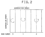
- Fig. 2 shows the bank configuration of a memory to be accessed by an address produced from the address generating circuit of the present invention.
- an address includes a high-order address and a low-order address, which are respectively expressed by high-order and low-order bits of an address value assigned to the address.
- a loop area is assigned such that a demarkation point of the loop is specified by the high-order address.
- the minimum width of the loop and the maximum number of banks are represented as 2 m and 2 l , respectively.
- the capacity of the low-order bits is equal to the width of each loop area, and the high-order bit designates one of the loop areas.
- the address generating circuit when the memory address is constituted as above, in response to an address specified by a distance d relative to a position indicated by a base pointer (BP) of an arbitrary loop area designated by a bank number, the address generating circuit creates an actual address associated with the specified address.
- BP base pointer
- Fig. 1 shows the structure of an address generator circuit in a first embodiment according to the present invention.
- a base pointer to be updated at an interval of a unit of period of time including a predetermined number of sampling periods (Fs) is commonly applied to all banks.
- the bank number is related to the high-order address, whereas information on the low-order address is common to all banks. Consequently, in order to update the content of a loop area depending on a bank number, there is required only one latch circuit for a base pointer.
- the address generator of Fig. 1 includes latch circuits 101 and 110, adders 102 and 104, EXOR gates 103 and 105, a loop width hold circuit 106, a bank number hold circuit 107, a coincidence detector circuit 108, and a selector circuit 109.
- the latch circuit 101 for a base pointer produces an output to be fed to one of the inputs of the adder 102.
- Another input of the adder 102 receives an output from the EXOR gate 103, the output being resultant from an EXOR operation accomplished between a specified distance d and a signal +/- denoting a direction in which the distance d is specified. Consequently, the adder 102 and the EXOR gate 103 can cooperatively accomplish an addition/subtraction processing.
- the adder 102 produces an output of address data by adding or subtracting the distance d relative to a position indicated by the base pointer to or from the value loaded in the base pointer depending on the specified direction.
- the loop width hold circuit 106 includes a memory in which bank widths are stored. When a bank number is specified, the hold circuit 106 outputs therefrom data indicating a band width of the specified bank to one of the inputs of the EXOR gate 105. Other one of the inputs thereof is supplied with a value obtained by inverting the +/- signal by an inverter 112.
- the EXOR gate 105 sends its output to one of the inputs of the adder 104.
- the other input of the adder 104 receives (1+2) bits of the high-order address of the address data delivered from the adder 102. Using these data items, the adder 104 and the EXOR gate 105 cooperatively carry out an addition or subtraction processing. This processing is conducted with an input of (1+2) bits including the high-order address, a carry in the addition/subtraction, and a sign.
- the bank number hold circuit 107 is a data hold circuit producing, based on the computation result from the adder 102, a signal indicating to which one of the loop areas the address data outputted from the adder 102 belongs. If there exists an area related to the address data, a bank number of the area is fed to the coincidence detector circuit 108. Otherwise, a signal causing the coincidence detector circuit 108 to produce an non-coincidence signal is delivered to the coincidence detector circuit 108.
- the coincidence detector circuit 108 compares the inputted bank number with that received from the bank number hold circuit 107 to determine whether or not these items match each other, thereby transferring a selection signal to the selector circuit 109.
- the selector circuit 109 selects and outputs the signal created from the adder 102 or the computation result from the adder 104 depending on whether the coincidence is detected or not, respectively. That is, if the bank number obtained by an address generated from the adder 102 is equal to the specified bank number, the address received from the adder 102 is directly outputted from the selector circuit 109. Otherwise, the loop width is increased or decreased through an addition or a subtraction by the adder circuit 104 to attain an address indicating the specified bank and then the address is outputed from the selector circuit 109.
- the latch circuit 110 latches m bits associated with the low-order address resultant from the computation of the adder 102 together with one bit selected by the selector circuit 109.
- the first adder/subtracter i.e. the adder 102 receives 43H and 45H through its respective input terminals.
- the adder 102 resultantly produces an output "088H".
- the bit width of the computation result "088H” is larger than the address bit width by two bits.
- Three high-order bits of the computation result "088H” are fed to the bank number hold circuit 107. In this case, the bank number is two.
- the coincidence detector circuit 108 compares the inputted bank number with an output from the bank number hold circuit 107. Since these input items match each other, the selector circuit 109 selects the output from the adder 102. In consequence, an address "88H" is latched by the latch circuit 110.
- the adder 102 outputs a value 0E9H.
- Three high-order bits "07H" are supplied to the second adder/subtracter circuit i.e. the adder 104.
- the loop width hold circuit 106 outputs a value 4H and hence the adder 104 produces a value 3H to be fed to the selector circuit 109.
- the selector circuit 109 selects and outputs the computation results from the adder 104.
- the address latch circuit 110 latches, as an actual address, a result "69H" obtained by adding 03H to the five low-order bits.
- an address can be specified by designating a bank number and a distance relative to a position denoted by a base pointer of the bank.
- the amount of hardware components can be minimized when compared with the conventional example as described above. For example, like in the conventional case, when the address pointer includes eight bits, namely, when four loop areas are allocated in a 256-word RAM, the base pointer occupies a word and only 128 transistors are required. That is, the number of transistors is minimized to one fourth as compared with the configuration of the prior art. When n areas are allocated, the number is reduced to 1/n of that of the conventional system.
- the circuit for correcting the address in a loop or in a periodic manner is constituted with a (1+2) -bit adder, a 1-bit coincidence detector circuit, and a RAM loaded with bank numbers. Namely, the hardware size is reduced when compared with the conventional circuit configuration. In addition, the processing speed of the address computation is resultantly increased.
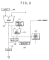
- Fig. 3 shows the configuration of an address generating circuit in a second embodiment in accordance with the present invention.
- the loop width is identical for all banks and the distance d is specified in the positive direction relative to a position indicated by the base pointer.
- the loop width is set as a constant to a constant hold circuit 111 such that the loop width is supplied to the subtracter 404, the addressing is achieved in a manner similar to that of the first embodiment.
- the address generating circuit can be constituted with a reduced amount of hardware components, which minimizes the cost thereof and increases the processing speed.
Landscapes
- Engineering & Computer Science (AREA)
- Theoretical Computer Science (AREA)
- Software Systems (AREA)
- Physics & Mathematics (AREA)
- General Engineering & Computer Science (AREA)
- General Physics & Mathematics (AREA)
- Complex Calculations (AREA)
- Memory System (AREA)
Applications Claiming Priority (2)
| Application Number | Priority Date | Filing Date | Title |
|---|---|---|---|
| JP417198/90 | 1990-12-29 | ||
| JP41719890A JP2692384B2 (ja) | 1990-12-29 | 1990-12-29 | アドレス生成回路 |
Publications (3)
| Publication Number | Publication Date |
|---|---|
| EP0493834A2 true EP0493834A2 (fr) | 1992-07-08 |
| EP0493834A3 EP0493834A3 (en) | 1993-03-17 |
| EP0493834B1 EP0493834B1 (fr) | 1998-11-04 |
Family
ID=18525324
Family Applications (1)
| Application Number | Title | Priority Date | Filing Date |
|---|---|---|---|
| EP91122380A Expired - Lifetime EP0493834B1 (fr) | 1990-12-29 | 1991-12-30 | Circuit générateur d'adresses |
Country Status (4)
| Country | Link |
|---|---|
| US (1) | US5471600A (fr) |
| EP (1) | EP0493834B1 (fr) |
| JP (1) | JP2692384B2 (fr) |
| DE (1) | DE69130448T2 (fr) |
Cited By (3)
| Publication number | Priority date | Publication date | Assignee | Title |
|---|---|---|---|---|
| EP0893755A3 (fr) * | 1997-07-21 | 2000-01-26 | Siemens Aktiengesellschaft | Dispositif de mémoire tampon |
| WO2001044921A2 (fr) | 1999-12-17 | 2001-06-21 | Koninklijke Philips Electronics N.V. | Registre d'adresse circulaire |
| WO2002054227A1 (fr) * | 2000-12-29 | 2002-07-11 | Intel Corporation | Adressage modulo |
Families Citing this family (24)
| Publication number | Priority date | Publication date | Assignee | Title |
|---|---|---|---|---|
| US5390304A (en) * | 1990-09-28 | 1995-02-14 | Texas Instruments, Incorporated | Method and apparatus for processing block instructions in a data processor |
| JPH064458A (ja) * | 1992-06-18 | 1994-01-14 | Fuji Xerox Co Ltd | Dma制御装置 |
| US5960212A (en) * | 1996-04-03 | 1999-09-28 | Telefonaktiebolaget Lm Ericsson (Publ) | Universal input/output controller having a unique coprocessor architecture |
| US5956665A (en) | 1996-11-15 | 1999-09-21 | Digital Equipment Corporation | Automatic mapping, monitoring, and control of computer room components |
| US5790782A (en) * | 1996-11-15 | 1998-08-04 | Digital Equipment Corporation | Automatic disk drive shelf address assignment and error detection method and apparatus |
| US6643744B1 (en) * | 2000-08-23 | 2003-11-04 | Nintendo Co., Ltd. | Method and apparatus for pre-fetching audio data |
| US6604169B2 (en) | 2001-06-01 | 2003-08-05 | Microchip Technology Incorporated | Modulo addressing based on absolute offset |
| US7020788B2 (en) | 2001-06-01 | 2006-03-28 | Microchip Technology Incorporated | Reduced power option |
| US6975679B2 (en) | 2001-06-01 | 2005-12-13 | Microchip Technology Incorporated | Configuration fuses for setting PWM options |
| US20020184566A1 (en) | 2001-06-01 | 2002-12-05 | Michael Catherwood | Register pointer trap |
| US6728856B2 (en) | 2001-06-01 | 2004-04-27 | Microchip Technology Incorporated | Modified Harvard architecture processor having program memory space mapped to data memory space |
| US6552625B2 (en) | 2001-06-01 | 2003-04-22 | Microchip Technology Inc. | Processor with pulse width modulation generator with fault input prioritization |
| US6601160B2 (en) | 2001-06-01 | 2003-07-29 | Microchip Technology Incorporated | Dynamically reconfigurable data space |
| US6952711B2 (en) | 2001-06-01 | 2005-10-04 | Microchip Technology Incorporated | Maximally negative signed fractional number multiplication |
| US7003543B2 (en) | 2001-06-01 | 2006-02-21 | Microchip Technology Incorporated | Sticky z bit |
| US6985986B2 (en) | 2001-06-01 | 2006-01-10 | Microchip Technology Incorporated | Variable cycle interrupt disabling |
| US6937084B2 (en) | 2001-06-01 | 2005-08-30 | Microchip Technology Incorporated | Processor with dual-deadtime pulse width modulation generator |
| US6976158B2 (en) | 2001-06-01 | 2005-12-13 | Microchip Technology Incorporated | Repeat instruction with interrupt |
| US7467178B2 (en) | 2001-06-01 | 2008-12-16 | Microchip Technology Incorporated | Dual mode arithmetic saturation processing |
| US7007172B2 (en) | 2001-06-01 | 2006-02-28 | Microchip Technology Incorporated | Modified Harvard architecture processor having data memory space mapped to program memory space with erroneous execution protection |
| US6934728B2 (en) | 2001-06-01 | 2005-08-23 | Microchip Technology Incorporated | Euclidean distance instructions |
| US20040021483A1 (en) * | 2001-09-28 | 2004-02-05 | Brian Boles | Functional pathway configuration at a system/IC interface |
| US6552567B1 (en) | 2001-09-28 | 2003-04-22 | Microchip Technology Incorporated | Functional pathway configuration at a system/IC interface |
| KR20160011015A (ko) * | 2014-07-21 | 2016-01-29 | 에스케이하이닉스 주식회사 | 어드레스 생성회로 및 이를 포함하는 메모리 장치 |
Family Cites Families (7)
| Publication number | Priority date | Publication date | Assignee | Title |
|---|---|---|---|---|
| GB1499184A (en) * | 1974-04-13 | 1978-01-25 | Mathematik & Datenverarbeitung | Circuit arrangement for monitoring the state of memory segments |
| GB2084362B (en) * | 1980-09-19 | 1984-07-11 | Solartron Electronic Group | Apparatus for performing the discrete fourier transform |
| US4602328A (en) * | 1982-12-17 | 1986-07-22 | L'etat Francais Represente Par Le Ministre Des P.T.T. (Centre National D'etudes Des Telecommunications) | Management system for the memory of a processor or microprocessor |
| JPS59128670A (ja) * | 1983-01-12 | 1984-07-24 | Hitachi Ltd | ベクトル処理装置 |
| US5083267A (en) * | 1987-05-01 | 1992-01-21 | Hewlett-Packard Company | Horizontal computer having register multiconnect for execution of an instruction loop with recurrance |
| JPH01265347A (ja) * | 1988-04-18 | 1989-10-23 | Matsushita Electric Ind Co Ltd | アドレス生成装置 |
| US5150471A (en) * | 1989-04-20 | 1992-09-22 | Ncr Corporation | Method and apparatus for offset register address accessing |
-
1990
- 1990-12-29 JP JP41719890A patent/JP2692384B2/ja not_active Expired - Fee Related
-
1991
- 1991-12-30 EP EP91122380A patent/EP0493834B1/fr not_active Expired - Lifetime
- 1991-12-30 DE DE69130448T patent/DE69130448T2/de not_active Expired - Fee Related
-
1995
- 1995-02-22 US US08/392,420 patent/US5471600A/en not_active Expired - Lifetime
Cited By (7)
| Publication number | Priority date | Publication date | Assignee | Title |
|---|---|---|---|---|
| EP0893755A3 (fr) * | 1997-07-21 | 2000-01-26 | Siemens Aktiengesellschaft | Dispositif de mémoire tampon |
| US6421770B1 (en) | 1997-07-21 | 2002-07-16 | Infineon Technologies Ag | Buffer memory configuration having a memory between a USB and a CPU |
| WO2001044921A2 (fr) | 1999-12-17 | 2001-06-21 | Koninklijke Philips Electronics N.V. | Registre d'adresse circulaire |
| WO2001044921A3 (fr) * | 1999-12-17 | 2001-11-08 | Koninkl Philips Electronics Nv | Registre d'adresse circulaire |
| WO2002054227A1 (fr) * | 2000-12-29 | 2002-07-11 | Intel Corporation | Adressage modulo |
| US6760830B2 (en) | 2000-12-29 | 2004-07-06 | Intel Corporation | Modulo addressing |
| KR100571327B1 (ko) * | 2000-12-29 | 2006-04-17 | 인텔 코포레이션 | 모듈로 어드레싱 방법 및 장치 |
Also Published As
| Publication number | Publication date |
|---|---|
| JPH04230545A (ja) | 1992-08-19 |
| EP0493834A3 (en) | 1993-03-17 |
| US5471600A (en) | 1995-11-28 |
| DE69130448T2 (de) | 1999-07-15 |
| EP0493834B1 (fr) | 1998-11-04 |
| JP2692384B2 (ja) | 1997-12-17 |
| DE69130448D1 (de) | 1998-12-10 |
Similar Documents
| Publication | Publication Date | Title |
|---|---|---|
| EP0493834B1 (fr) | Circuit générateur d'adresses | |
| US4742479A (en) | Modulo arithmetic unit having arbitrary offset and modulo values | |
| US5623621A (en) | Apparatus for generating target addresses within a circular buffer including a register for storing position and size of the circular buffer | |
| US4823301A (en) | Method and circuit for computing reciprocals | |
| EP0372566A2 (fr) | Circuit arithmétique pour obtenir la valeur réciproque à l'aide d'une table stockée dans une mémoire morte | |
| JPH05113930A (ja) | フレキシブルなn−ウエイ・メモリ・インターリーブ方式 | |
| EP0530372A1 (fr) | Convertisseur d'expression numerique et processeur vectoriel l'utilisant | |
| KR100398859B1 (ko) | 데이터 연산 처리 장치 | |
| US6065031A (en) | Log converter utilizing offset and method of use thereof | |
| US5319347A (en) | Parallelized magnitude comparator for comparing a binary number to a fixed value | |
| US4718032A (en) | Method and apparatus for effecting range transformation in a digital circuitry | |
| US5383142A (en) | Fast circuit and method for detecting predetermined bit patterns | |
| US5079736A (en) | High speed pipeline merge sorter with run length tuning mechanism | |
| EP0555382B1 (fr) | Generateur d'adresses pour memoire tampon circulaire | |
| EP0637797A1 (fr) | Appareil à calculer | |
| US5974436A (en) | Execution processor for carrying out power calculation | |
| EP0606775A1 (fr) | Système et procédé pour l'approximation de fonctions non-linéaires | |
| US4130876A (en) | Method of and apparatus for composing approximate sinusoidal waveform | |
| JP2509279B2 (ja) | 浮動小数点数一固定小数点数変換装置 | |
| US4941118A (en) | Division circuit having an operation loop including an adder and multiplier | |
| EP0568373A2 (fr) | Comparateur de magnitude en parallèle | |
| JP3538512B2 (ja) | データ変換装置 | |
| JP2732673B2 (ja) | 離散的コサイン変換装置 | |
| EP0702290B1 (fr) | Dispositif de division numérique utilisant une table de consultation | |
| US6052768A (en) | Circuit and method for modulo address generation with reduced circuit area |
Legal Events
| Date | Code | Title | Description |
|---|---|---|---|
| PUAI | Public reference made under article 153(3) epc to a published international application that has entered the european phase |
Free format text: ORIGINAL CODE: 0009012 |
|
| AK | Designated contracting states |
Kind code of ref document: A2 Designated state(s): DE FR GB |
|
| 17P | Request for examination filed |
Effective date: 19920629 |
|
| PUAL | Search report despatched |
Free format text: ORIGINAL CODE: 0009013 |
|
| AK | Designated contracting states |
Kind code of ref document: A3 Designated state(s): DE FR GB |
|
| 17Q | First examination report despatched |
Effective date: 19961216 |
|
| GRAG | Despatch of communication of intention to grant |
Free format text: ORIGINAL CODE: EPIDOS AGRA |
|
| GRAG | Despatch of communication of intention to grant |
Free format text: ORIGINAL CODE: EPIDOS AGRA |
|
| GRAH | Despatch of communication of intention to grant a patent |
Free format text: ORIGINAL CODE: EPIDOS IGRA |
|
| GRAH | Despatch of communication of intention to grant a patent |
Free format text: ORIGINAL CODE: EPIDOS IGRA |
|
| GRAA | (expected) grant |
Free format text: ORIGINAL CODE: 0009210 |
|
| AK | Designated contracting states |
Kind code of ref document: B1 Designated state(s): DE FR GB |
|
| REF | Corresponds to: |
Ref document number: 69130448 Country of ref document: DE Date of ref document: 19981210 |
|
| ET | Fr: translation filed | ||
| PLBE | No opposition filed within time limit |
Free format text: ORIGINAL CODE: 0009261 |
|
| STAA | Information on the status of an ep patent application or granted ep patent |
Free format text: STATUS: NO OPPOSITION FILED WITHIN TIME LIMIT |
|
| 26N | No opposition filed | ||
| REG | Reference to a national code |
Ref country code: GB Ref legal event code: IF02 |
|
| REG | Reference to a national code |
Ref country code: GB Ref legal event code: 732E |
|
| REG | Reference to a national code |
Ref country code: FR Ref legal event code: TP |
|
| PGFP | Annual fee paid to national office [announced via postgrant information from national office to epo] |
Ref country code: GB Payment date: 20071227 Year of fee payment: 17 Ref country code: FR Payment date: 20071210 Year of fee payment: 17 |
|
| PGFP | Annual fee paid to national office [announced via postgrant information from national office to epo] |
Ref country code: DE Payment date: 20071231 Year of fee payment: 17 |
|
| GBPC | Gb: european patent ceased through non-payment of renewal fee |
Effective date: 20081230 |
|
| REG | Reference to a national code |
Ref country code: FR Ref legal event code: ST Effective date: 20090831 |
|
| PG25 | Lapsed in a contracting state [announced via postgrant information from national office to epo] |
Ref country code: DE Free format text: LAPSE BECAUSE OF NON-PAYMENT OF DUE FEES Effective date: 20090701 |
|
| PG25 | Lapsed in a contracting state [announced via postgrant information from national office to epo] |
Ref country code: GB Free format text: LAPSE BECAUSE OF NON-PAYMENT OF DUE FEES Effective date: 20081230 |
|
| PG25 | Lapsed in a contracting state [announced via postgrant information from national office to epo] |
Ref country code: FR Free format text: LAPSE BECAUSE OF NON-PAYMENT OF DUE FEES Effective date: 20081231 |