EP0496406A2 - Halbleiterspeicheranordnung - Google Patents
Halbleiterspeicheranordnung Download PDFInfo
- Publication number
- EP0496406A2 EP0496406A2 EP92101102A EP92101102A EP0496406A2 EP 0496406 A2 EP0496406 A2 EP 0496406A2 EP 92101102 A EP92101102 A EP 92101102A EP 92101102 A EP92101102 A EP 92101102A EP 0496406 A2 EP0496406 A2 EP 0496406A2
- Authority
- EP
- European Patent Office
- Prior art keywords
- peripheral circuits
- memory cell
- cell forming
- bit line
- forming regions
- Prior art date
- Legal status (The legal status is an assumption and is not a legal conclusion. Google has not performed a legal analysis and makes no representation as to the accuracy of the status listed.)
- Granted
Links
Images






Classifications
-
- G—PHYSICS
- G11—INFORMATION STORAGE
- G11C—STATIC STORES
- G11C11/00—Digital stores characterised by the use of particular electric or magnetic storage elements; Storage elements therefor
- G11C11/21—Digital stores characterised by the use of particular electric or magnetic storage elements; Storage elements therefor using electric elements
- G11C11/34—Digital stores characterised by the use of particular electric or magnetic storage elements; Storage elements therefor using electric elements using semiconductor devices
- G11C11/40—Digital stores characterised by the use of particular electric or magnetic storage elements; Storage elements therefor using electric elements using semiconductor devices using transistors
-
- G—PHYSICS
- G11—INFORMATION STORAGE
- G11C—STATIC STORES
- G11C5/00—Details of stores covered by group G11C11/00
- G11C5/02—Disposition of storage elements, e.g. in the form of a matrix array
- G11C5/025—Geometric lay-out considerations of storage- and peripheral-blocks in a semiconductor storage device
-
- G—PHYSICS
- G11—INFORMATION STORAGE
- G11C—STATIC STORES
- G11C11/00—Digital stores characterised by the use of particular electric or magnetic storage elements; Storage elements therefor
- G11C11/21—Digital stores characterised by the use of particular electric or magnetic storage elements; Storage elements therefor using electric elements
- G11C11/34—Digital stores characterised by the use of particular electric or magnetic storage elements; Storage elements therefor using electric elements using semiconductor devices
- G11C11/40—Digital stores characterised by the use of particular electric or magnetic storage elements; Storage elements therefor using electric elements using semiconductor devices using transistors
- G11C11/401—Digital stores characterised by the use of particular electric or magnetic storage elements; Storage elements therefor using electric elements using semiconductor devices using transistors forming cells needing refreshing or charge regeneration, i.e. dynamic cells
- G11C11/4063—Auxiliary circuits, e.g. for addressing, decoding, driving, writing, sensing or timing
- G11C11/407—Auxiliary circuits, e.g. for addressing, decoding, driving, writing, sensing or timing for memory cells of the field-effect type
- G11C11/409—Read-write [R-W] circuits
- G11C11/4097—Bit-line organisation, e.g. bit-line layout, folded bit lines
-
- Y—GENERAL TAGGING OF NEW TECHNOLOGICAL DEVELOPMENTS; GENERAL TAGGING OF CROSS-SECTIONAL TECHNOLOGIES SPANNING OVER SEVERAL SECTIONS OF THE IPC; TECHNICAL SUBJECTS COVERED BY FORMER USPC CROSS-REFERENCE ART COLLECTIONS [XRACs] AND DIGESTS
- Y10—TECHNICAL SUBJECTS COVERED BY FORMER USPC
- Y10S—TECHNICAL SUBJECTS COVERED BY FORMER USPC CROSS-REFERENCE ART COLLECTIONS [XRACs] AND DIGESTS
- Y10S257/00—Active solid-state devices, e.g. transistors, solid-state diodes
- Y10S257/922—Active solid-state devices, e.g. transistors, solid-state diodes with means to prevent inspection of or tampering with an integrated circuit, e.g. "smart card", anti-tamper
Definitions
- the present invention relates to a semiconductor apparatus, and more particularly to the arrangement of circuits peripheral to a dynamic random access memory (DRAM).
- DRAM dynamic random access memory
- a semiconductor memory apparatus such as a DRAM
- a semiconductor memory apparatus consists of memory cell array forming sections, formed by arranging memory cells, and peripheral circuits adjacent to it, including sense amplifiers, row decoders and column decoders.
- peripheral circuits specific items such as sense amplifiers, one of which is provided for each pair of bit lines to each of which is supplied a voltage in a complementary relationship to each one of a plurality of bit lines constituting the memory cell array, have to be installed at a rate of one unit per pair of bit lines. Therefore, these specific peripheral circuits are arranged along a side of said memory cell array forming sections.
- peripheral circuits for such system functions as serial data transfer and flash clear should be provided for each pair of said bit lines in order to realize these functions on said semiconductor chip.
- peripheral circuits used for said specialized semiconductor memory include line buffer circuits and serial switching circuits in addition to said sense amplifiers, resulting in a complex and large-scale configuration. Accordingly, it has become difficult to arrange these peripheral circuits along a side of said memory cell array forming sections at the repetitive pitch of said bit line pairs.
- peripheral circuits be arranged in disregard of said repetitive pitch, the characteristics of transistors, which are the constituent elements of the peripheral circuits, would become unmatched, and moreover said bit line pairs would be laid in an elongated state, resulting in large resistances and capacities added to the bit line pairs.
- an object of the present invention is to provide a semiconductor memory apparatus which is freed from a slowdown in writing and reading rates and the occurrence of erroneous operations by arranging its peripheral circuits by matching the characteristics of their constituent elements and balancing the lengths of bit line pairs.
- a semiconductor memory apparatus having on the surface of a semiconductor substrate: memory cell forming regions, each of a rectangular plane shape surrounded by first and second edges extending in a first direction and third and fourth edges extending in a second direction at a right angle to said first direction; memory cell forming sections in each of which a plurality of said memory cell forming regions are arranged in said first direction; a plurality of memory cells arranged and formed in each of said memory cell forming regions; first and second bit line pairs connecting respectively corresponding ones of said plurality of memory cells in said memory cell forming regions and formed extending in said second direction in said regions; first peripheral circuits formed outside said memory cell forming regions along and opposite to said first edge and having first and second connecting points; and second peripheral circuits formed outside said memory cell forming regions along and opposite to said second edge and having first and second connecting points; wherein said first and second peripheral circuits are arranged and formed symmetrically with respect to the point of intersection between a first centerline connecting the middle point of said first edge and that of said
- first and second peripheral circuits may further be arranged a plurality of mutually adjoining first and second peripheral circuits, respectively in orthogonal symmetry.
- a semiconductor chip 7 constituting a semiconductor memory apparatus which is a first preferred embodiment of the present invention, involves memory cell forming sections 6 in which memory cells are arranged in arrays, a row decoder 5 which selects a word line according to the input address, bit line balancing circuits 3 which balance each bit line pair at the same potential, bit line potential supplying circuits 4, and peripheral circuit sections 1 each having a sense amplifier 2 (although this semiconductor memory apparatus also has other circuits in its peripheral circuit sections, they are not referred to here for the convenience of description).
- Each peripheral circuit section 1 containing a sense amplifier 2 is arranged close to a memory cell forming section 6 because it is connected to a bit line pair making up a part of the memory cell forming section 6. More specifically, peripheral circuit sections 1 are arranged along two mutually parallel sides of the memory cell forming section 6 and outside the memory cell forming section 6.
- a memory cell forming section 6 in this preferred embodiment consists of a plurality of memory cells (MC's) arranged in an array, each cell comprising an N-channel transistor and a capacity element (i.e. it is formed by arranging so-called one-transistor one-capacitor type MC's in an array).
- MC memory cells
- a word line such as WL-1, WL-2, ... or WL-n
- bit lines such as BLa1/BLb1, BLa2/BLb2, ... or BLam/BLbm
- a sense amplifier SA (such as SA1, SA2, ... or the like) involved in the peripheral circuit section 1 consists of a flip-flop type circuit, balanced between two sides in terms of transistor characteristics and floating capacity among others.
- a P-channel transistor MP41 and an N-channel transistor MN41 constitute a first inverter circuit
- a P-channel transistor MP42 and an N-channel transistor MN42 constitute a second inverter circuit
- a flip-flop is composed by feeding back the outputs of the first and second inverter circuits to the inputs of the second and first inverter circuits.
- To the input of each of the first and second inverter circuits are connected a pair of bit lines BLa and BLb to constitute a sense amplifier 31.
- the gate electrode 51, formed of a polysilicon membrane, of the transistor MP41 is connected through a contact hole 41 to metallic wiring which forms the bit line BLa, and the source-drain path of the same transistor MP41 is connected through a contact hole 45 to metallic wiring which forms the bit line BLb and a signal line SAP.
- the transistor MP42 is arranged matched with said transistor MP41.
- Its gate electrode 52, formed of a polysilicon membrane, is connected through a contact hole 42 to metallic wiring which forms the bit line BLb, and its source-drain path is connected through a contact hole 46 to metallic wiring which forms the bit line BLa and the signal line SAP.
- the gate electrode 54, formed of a polysilicon membrane, of the transistor MN41 is connected through a contact hole 44 to said bit line BLa, and the source-drain path of the same transistor MN41 is connected through a contact hole 47 to the bit line Blb and a signal line SAN.
- the transistor MN42 is arranged matched with said transistor MN4, with its electrode 53, formed of a polysilicon membrane, connected through a contact hole 43 to the bit line BLb, and its source-drain path connected through a contact hole 48 to said bit line BLa and the signal line SAN.
- the sense amplifier 31 is formed on the semiconductor chip in an arrangement matching the bit line pairs BLa and BLb. This sense amplifier 31 operates as appropriate potentials are given to the signal lines SAP and SAN by activating signals (not shown).
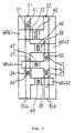
- peripheral circuits 15 and 16 both corresponding to a memory cell forming region 17 involving the (k+1)th bit line pairs BLa(k+1) and Blb(k+1), respectively adjoining the kth bit line pairs BLa(k) and BLb(k) in FIG. 2, are arranged outside the memory cell forming region 17 along edges 12 and 11, respectively, of the region 17. Further, said peripheral circuits 15 and 16 are formed in a symmetric arrangement with respect to the intersection point G of centerlines 18 and 19, respectively connecting the middle points of the edges 11 and 12 and those of edges 13 and 14.
- bit line pairs BLa (k) and BLb(k) are connected to the peripheral circuit 15 via connecting points P1 and P2 on a side of the peripheral circuit 15 opposite to said memory cell forming region 17.
- bit line pairs BLa (k+1) and BLb(k+1) are connected to the peripheral circuit 16 Via connecting points Q1 and Q2 on a side of the peripheral circuit 16 opposite to said memory cell forming region 17.
- FIG. 6 is a plan illustrating a part of the arrangement pattern, corresponding to FIG. 4, of a case in which the peripheral circuits 15 and 16 of FIG. 5 involve sense amplifiers 31 of FIG. 3.
- the same constituent parts as in FIG. 5 are assigned respectively the same reference numerals or codes.
- the metallic wiring patterns 61 and 62 of the sense amplifier involved in the peripheral circuit 15 are connected to the connecting points P1 and P2, and the metallic wiring patterns 63 and 64 of the sense amplifier involved in the peripheral circuit 16 are connected to the connecting points Q1 and Q2, the metallic wiring patterns 61 and 63 and the metallic wiring patterns 62 and 64 being respectively arranged symmetrically with respect to the intersection point G.
- precharge signals shift a signal line PDL from a high to a low level and turn off transistors MN10 and MN20.
- a word line WL-i selected by the row decoder 5 is activated.
- the stored contents of a plurality of MC's connected to the word line WL-i are supplied to the corresponding bit line pair.
- Either one of paired bit lines BLak and BLbk is reduced in potential to below that of a power supply line VHL according to the stored content of the MC, and the potential of the other is equalized to that of said power supply line VHL (if a low level is stored in the MC).
- SA sense amplifier
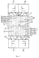
- Said peripheral circuits 75 and 76 are symmetrically arranged with respect to the intersection point G1 of a memory cell forming region 79 involving the (4k-3)th and (4k-2)th bit line pairs.
- the peripheral circuits 85 and 86 are symmetrically arranged with respect to the intersection point G2 of a memory cell forming region 80 involving the (4k-1)th and 4kth bit line pairs.
- said peripheral circuits 75 and 85 and said peripheral circuits 76 and 86 are symmetrically arranged with respect to the intersection point G of the memory cell forming region 77 involving these four bit line pairs.
- the peripheral circuits 75 and 85 and the peripheral circuits 76 and 86 are symmetrically formed with respect to a centerline which passes the intersection point G and is parallel to said edge 74 or 73.
- FIG. 8 is a plan illustrating a part of the arrangement pattern, corresponding to FIG. 4, of a case in which the peripheral circuits 75, 76, 85 and 86 of FIG. 7 involve sense amplifiers 31 of FIG. 3.
- the same constituent parts as in FIG. 7 are assigned respectively the same reference numerals or codes.
- the metallic wiring patterns 181, 182, 183 and 184 of the sense amplifiers involved in the peripheral circuits 75 and 85 are connected to the connecting points P11, P21, P31 and P41, and the metallic wiring patterns 185, 186, 187 and 188 of the sense amplifiers involved in the peripheral circuits 76 and 86 are connected to the connecting points Q11, Q21, Q31 and Q41, the metallic wiring patterns 181, 182, 183 and 184 and the metallic wiring patterns 185, 186, 187 and 188 being respectively arranged symmetrically with respect to the intersection point G.
- This semiconductor memory apparatus which is the second preferred embodiment of the invention, can be composed in an arrangement of formation in which peripheral circuits connected to consecutive four-bit bit line pairs are positioned at the top and bottom of the memory forming section, with each set comprising two bits.
- the constituent elements including sense amplifiers can be well matched with each other and so can be bit line pairs, making it possible to realize an error-free semiconductor memory apparatus, suffering no substantial drop in reading or writing rate.
- the response rate of the bit line pairs of a picture memory, for instance, according to the invention would be about 25 ns higher than that by the prior art, which means that a higher speed picture memory can be materialized.
Landscapes
- Engineering & Computer Science (AREA)
- Microelectronics & Electronic Packaging (AREA)
- Computer Hardware Design (AREA)
- Semiconductor Memories (AREA)
- Dram (AREA)
Applications Claiming Priority (2)
| Application Number | Priority Date | Filing Date | Title |
|---|---|---|---|
| JP2550691 | 1991-01-25 | ||
| JP25506/91 | 1991-01-25 |
Publications (3)
| Publication Number | Publication Date |
|---|---|
| EP0496406A2 true EP0496406A2 (de) | 1992-07-29 |
| EP0496406A3 EP0496406A3 (de) | 1994-03-16 |
| EP0496406B1 EP0496406B1 (de) | 1999-05-06 |
Family
ID=12167955
Family Applications (1)
| Application Number | Title | Priority Date | Filing Date |
|---|---|---|---|
| EP92101102A Expired - Lifetime EP0496406B1 (de) | 1991-01-25 | 1992-01-23 | Halbleiterspeicheranordnung |
Country Status (4)
| Country | Link |
|---|---|
| US (1) | US5315138A (de) |
| EP (1) | EP0496406B1 (de) |
| KR (1) | KR960001784B1 (de) |
| DE (1) | DE69229067T2 (de) |
Cited By (1)
| Publication number | Priority date | Publication date | Assignee | Title |
|---|---|---|---|---|
| EP0717414A3 (de) * | 1994-12-16 | 1996-11-06 | Toshiba Kk | Halbleiterspeicher |
Families Citing this family (1)
| Publication number | Priority date | Publication date | Assignee | Title |
|---|---|---|---|---|
| US7948094B2 (en) | 2007-10-22 | 2011-05-24 | Rohm Co., Ltd. | Semiconductor device |
Family Cites Families (5)
| Publication number | Priority date | Publication date | Assignee | Title |
|---|---|---|---|---|
| JPS538528A (en) * | 1976-07-12 | 1978-01-26 | Nec Corp | Memory circuit |
| US4506347A (en) * | 1981-02-20 | 1985-03-19 | Mostek Corporation | Placement of clock circuits for semiconductor memory |
| JPH0752757B2 (ja) * | 1985-04-12 | 1995-06-05 | 株式会社日立製作所 | 半導体記憶装置 |
| US4926224A (en) * | 1988-06-03 | 1990-05-15 | Texas Instruments Incorporated | Crosspoint dynamic ram cell for folded bitline array |
| JPH07109878B2 (ja) * | 1988-11-16 | 1995-11-22 | 株式会社東芝 | 半導体記憶装置 |
-
1992
- 1992-01-23 EP EP92101102A patent/EP0496406B1/de not_active Expired - Lifetime
- 1992-01-23 DE DE69229067T patent/DE69229067T2/de not_active Expired - Fee Related
- 1992-01-25 KR KR1019920001096A patent/KR960001784B1/ko not_active Expired - Fee Related
- 1992-01-27 US US07/826,419 patent/US5315138A/en not_active Expired - Fee Related
Cited By (2)
| Publication number | Priority date | Publication date | Assignee | Title |
|---|---|---|---|---|
| EP0717414A3 (de) * | 1994-12-16 | 1996-11-06 | Toshiba Kk | Halbleiterspeicher |
| US5691933A (en) * | 1994-12-16 | 1997-11-25 | Kabushiki Kaisha Toshiba | Semiconductor memory device having improved bit line distribution |
Also Published As
| Publication number | Publication date |
|---|---|
| DE69229067T2 (de) | 1999-12-09 |
| KR920015375A (ko) | 1992-08-26 |
| KR960001784B1 (ko) | 1996-02-05 |
| EP0496406B1 (de) | 1999-05-06 |
| EP0496406A3 (de) | 1994-03-16 |
| US5315138A (en) | 1994-05-24 |
| DE69229067D1 (de) | 1999-06-10 |
Similar Documents
| Publication | Publication Date | Title |
|---|---|---|
| US6504246B2 (en) | Integrated circuit having a balanced twist for differential signal lines | |
| KR100538883B1 (ko) | 반도체 메모리 장치 | |
| US5416734A (en) | Bit line structure for semiconductor memory device | |
| US4367540A (en) | Dynamic memory with an interchangeable pair of data lines and sense amplifiers | |
| US5111434A (en) | Semiconductor memory device | |
| US6084820A (en) | Dual port memory device with vertical shielding | |
| EP0505926B1 (de) | Multiport-Speicher | |
| US4872142A (en) | Semiconductor memory device with improved bit line arrangement | |
| US5097440A (en) | Semiconductor memory device comprising a plurality of memory arrays with improved peripheral circuit location and interconnection arrangement | |
| EP0107387A2 (de) | Halbleiterspeicheranordnung | |
| KR850007158A (ko) | 반도체 메모리 장치 | |
| US4418399A (en) | Semiconductor memory system | |
| USRE36169E (en) | Semiconductor memory device | |
| US4578780A (en) | Dual port type semiconductor memory | |
| US6118708A (en) | Semiconductor memory device | |
| EP0502398B1 (de) | Dynamische Speichereinrichtung mit wahlfreiem Zugriff, mit Bitleitungen, die zwischen den Leseverstärkerschaltungen teilweise gemeinsam benutzt werden | |
| US20060158918A1 (en) | Semiconductor memory device | |
| US5184321A (en) | Semiconductor memory device comprising a plurality of memory arrays with improved peripheral circuit location and interconnection arrangement | |
| US5375097A (en) | Segmented bus architecture for improving speed in integrated circuit memories | |
| US5315138A (en) | Semiconductor memory apparatus | |
| US20240321344A1 (en) | Sram device including buried bit line and buried word line using backside metal | |
| JPS59217290A (ja) | 半導体メモリ | |
| US6721221B2 (en) | Sense amplifier and architecture for open digit arrays | |
| JPH0582746A (ja) | 半導体記憶装置 | |
| US7433259B2 (en) | Semiconductor memory device having layered bit line structure |
Legal Events
| Date | Code | Title | Description |
|---|---|---|---|
| PUAI | Public reference made under article 153(3) epc to a published international application that has entered the european phase |
Free format text: ORIGINAL CODE: 0009012 |
|
| 17P | Request for examination filed |
Effective date: 19920123 |
|
| AK | Designated contracting states |
Kind code of ref document: A2 Designated state(s): DE FR GB |
|
| PUAL | Search report despatched |
Free format text: ORIGINAL CODE: 0009013 |
|
| AK | Designated contracting states |
Kind code of ref document: A3 Designated state(s): DE FR GB |
|
| 17Q | First examination report despatched |
Effective date: 19950710 |
|
| GRAG | Despatch of communication of intention to grant |
Free format text: ORIGINAL CODE: EPIDOS AGRA |
|
| GRAG | Despatch of communication of intention to grant |
Free format text: ORIGINAL CODE: EPIDOS AGRA |
|
| GRAH | Despatch of communication of intention to grant a patent |
Free format text: ORIGINAL CODE: EPIDOS IGRA |
|
| GRAH | Despatch of communication of intention to grant a patent |
Free format text: ORIGINAL CODE: EPIDOS IGRA |
|
| GRAA | (expected) grant |
Free format text: ORIGINAL CODE: 0009210 |
|
| AK | Designated contracting states |
Kind code of ref document: B1 Designated state(s): DE FR GB |
|
| REF | Corresponds to: |
Ref document number: 69229067 Country of ref document: DE Date of ref document: 19990610 |
|
| ET | Fr: translation filed | ||
| PLBE | No opposition filed within time limit |
Free format text: ORIGINAL CODE: 0009261 |
|
| STAA | Information on the status of an ep patent application or granted ep patent |
Free format text: STATUS: NO OPPOSITION FILED WITHIN TIME LIMIT |
|
| 26N | No opposition filed | ||
| REG | Reference to a national code |
Ref country code: GB Ref legal event code: IF02 |
|
| REG | Reference to a national code |
Ref country code: GB Ref legal event code: 732E |
|
| REG | Reference to a national code |
Ref country code: FR Ref legal event code: TP |
|
| PGFP | Annual fee paid to national office [announced via postgrant information from national office to epo] |
Ref country code: FR Payment date: 20050110 Year of fee payment: 14 |
|
| PGFP | Annual fee paid to national office [announced via postgrant information from national office to epo] |
Ref country code: GB Payment date: 20050119 Year of fee payment: 14 |
|
| PGFP | Annual fee paid to national office [announced via postgrant information from national office to epo] |
Ref country code: DE Payment date: 20050120 Year of fee payment: 14 |
|
| PG25 | Lapsed in a contracting state [announced via postgrant information from national office to epo] |
Ref country code: GB Free format text: LAPSE BECAUSE OF NON-PAYMENT OF DUE FEES Effective date: 20060123 |
|
| PG25 | Lapsed in a contracting state [announced via postgrant information from national office to epo] |
Ref country code: FR Free format text: LAPSE BECAUSE OF NON-PAYMENT OF DUE FEES Effective date: 20060131 |
|
| PG25 | Lapsed in a contracting state [announced via postgrant information from national office to epo] |
Ref country code: DE Free format text: LAPSE BECAUSE OF NON-PAYMENT OF DUE FEES Effective date: 20060801 |
|
| GBPC | Gb: european patent ceased through non-payment of renewal fee |
Effective date: 20060123 |
|
| REG | Reference to a national code |
Ref country code: FR Ref legal event code: ST Effective date: 20060929 |