EP0496718B1 - Méthode pour minimiser les pertes de commutation dans un commutateur de puissance - Google Patents
Méthode pour minimiser les pertes de commutation dans un commutateur de puissance Download PDFInfo
- Publication number
- EP0496718B1 EP0496718B1 EP92870011A EP92870011A EP0496718B1 EP 0496718 B1 EP0496718 B1 EP 0496718B1 EP 92870011 A EP92870011 A EP 92870011A EP 92870011 A EP92870011 A EP 92870011A EP 0496718 B1 EP0496718 B1 EP 0496718B1
- Authority
- EP
- European Patent Office
- Prior art keywords
- power switch
- switching
- switch
- controlled power
- voltage
- Prior art date
- Legal status (The legal status is an assumption and is not a legal conclusion. Google has not performed a legal analysis and makes no representation as to the accuracy of the status listed.)
- Expired - Lifetime
Links
Images



Classifications
-
- H—ELECTRICITY
- H02—GENERATION; CONVERSION OR DISTRIBUTION OF ELECTRIC POWER
- H02M—APPARATUS FOR CONVERSION BETWEEN AC AND AC, BETWEEN AC AND DC, OR BETWEEN DC AND DC, AND FOR USE WITH MAINS OR SIMILAR POWER SUPPLY SYSTEMS; CONVERSION OF DC OR AC INPUT POWER INTO SURGE OUTPUT POWER; CONTROL OR REGULATION THEREOF
- H02M1/00—Details of apparatus for conversion
- H02M1/32—Means for protecting converters other than automatic disconnection
- H02M1/34—Snubber circuits
-
- H—ELECTRICITY
- H02—GENERATION; CONVERSION OR DISTRIBUTION OF ELECTRIC POWER
- H02M—APPARATUS FOR CONVERSION BETWEEN AC AND AC, BETWEEN AC AND DC, OR BETWEEN DC AND DC, AND FOR USE WITH MAINS OR SIMILAR POWER SUPPLY SYSTEMS; CONVERSION OF DC OR AC INPUT POWER INTO SURGE OUTPUT POWER; CONTROL OR REGULATION THEREOF
- H02M3/00—Conversion of DC power input into DC power output
- H02M3/02—Conversion of DC power input into DC power output without intermediate conversion into AC
- H02M3/04—Conversion of DC power input into DC power output without intermediate conversion into AC by static converters
- H02M3/10—Conversion of DC power input into DC power output without intermediate conversion into AC by static converters using discharge tubes with control electrode or semiconductor devices with control electrode
- H02M3/145—Conversion of DC power input into DC power output without intermediate conversion into AC by static converters using discharge tubes with control electrode or semiconductor devices with control electrode using devices of a triode or transistor type requiring continuous application of a control signal
- H02M3/155—Conversion of DC power input into DC power output without intermediate conversion into AC by static converters using discharge tubes with control electrode or semiconductor devices with control electrode using devices of a triode or transistor type requiring continuous application of a control signal using semiconductor devices only
- H02M3/156—Conversion of DC power input into DC power output without intermediate conversion into AC by static converters using discharge tubes with control electrode or semiconductor devices with control electrode using devices of a triode or transistor type requiring continuous application of a control signal using semiconductor devices only with automatic control of output voltage or current, e.g. switching regulators
- H02M3/158—Conversion of DC power input into DC power output without intermediate conversion into AC by static converters using discharge tubes with control electrode or semiconductor devices with control electrode using devices of a triode or transistor type requiring continuous application of a control signal using semiconductor devices only with automatic control of output voltage or current, e.g. switching regulators including plural semiconductor devices as final control devices for a single load
-
- H—ELECTRICITY
- H02—GENERATION; CONVERSION OR DISTRIBUTION OF ELECTRIC POWER
- H02M—APPARATUS FOR CONVERSION BETWEEN AC AND AC, BETWEEN AC AND DC, OR BETWEEN DC AND DC, AND FOR USE WITH MAINS OR SIMILAR POWER SUPPLY SYSTEMS; CONVERSION OF DC OR AC INPUT POWER INTO SURGE OUTPUT POWER; CONTROL OR REGULATION THEREOF
- H02M3/00—Conversion of DC power input into DC power output
- H02M3/22—Conversion of DC power input into DC power output with intermediate conversion into AC
- H02M3/24—Conversion of DC power input into DC power output with intermediate conversion into AC by static converters
- H02M3/28—Conversion of DC power input into DC power output with intermediate conversion into AC by static converters using discharge tubes with control electrode or semiconductor devices with control electrode to produce the intermediate AC
- H02M3/325—Conversion of DC power input into DC power output with intermediate conversion into AC by static converters using discharge tubes with control electrode or semiconductor devices with control electrode to produce the intermediate AC using devices of a triode or a transistor type requiring continuous application of a control signal
- H02M3/335—Conversion of DC power input into DC power output with intermediate conversion into AC by static converters using discharge tubes with control electrode or semiconductor devices with control electrode to produce the intermediate AC using devices of a triode or a transistor type requiring continuous application of a control signal using semiconductor devices only
- H02M3/33569—Conversion of DC power input into DC power output with intermediate conversion into AC by static converters using discharge tubes with control electrode or semiconductor devices with control electrode to produce the intermediate AC using devices of a triode or a transistor type requiring continuous application of a control signal using semiconductor devices only having several active switching elements
-
- H—ELECTRICITY
- H03—ELECTRONIC CIRCUITRY
- H03K—PULSE TECHNIQUE
- H03K17/00—Electronic switching or gating, i.e. not by contact-making and –breaking
- H03K17/04—Modifications for accelerating switching
- H03K17/041—Modifications for accelerating switching without feedback from the output circuit to the control circuit
- H03K17/0416—Modifications for accelerating switching without feedback from the output circuit to the control circuit by measures taken in the output circuit
- H03K17/04163—Modifications for accelerating switching without feedback from the output circuit to the control circuit by measures taken in the output circuit in field-effect transistor switches
-
- H—ELECTRICITY
- H03—ELECTRONIC CIRCUITRY
- H03K—PULSE TECHNIQUE
- H03K17/00—Electronic switching or gating, i.e. not by contact-making and –breaking
- H03K17/08—Modifications for protecting switching circuit against overcurrent or overvoltage
- H03K17/081—Modifications for protecting switching circuit against overcurrent or overvoltage without feedback from the output circuit to the control circuit
- H03K17/0814—Modifications for protecting switching circuit against overcurrent or overvoltage without feedback from the output circuit to the control circuit by measures taken in the output circuit
- H03K17/08142—Modifications for protecting switching circuit against overcurrent or overvoltage without feedback from the output circuit to the control circuit by measures taken in the output circuit in field-effect transistor switches
-
- H—ELECTRICITY
- H02—GENERATION; CONVERSION OR DISTRIBUTION OF ELECTRIC POWER
- H02M—APPARATUS FOR CONVERSION BETWEEN AC AND AC, BETWEEN AC AND DC, OR BETWEEN DC AND DC, AND FOR USE WITH MAINS OR SIMILAR POWER SUPPLY SYSTEMS; CONVERSION OF DC OR AC INPUT POWER INTO SURGE OUTPUT POWER; CONTROL OR REGULATION THEREOF
- H02M1/00—Details of apparatus for conversion
- H02M1/32—Means for protecting converters other than automatic disconnection
- H02M1/34—Snubber circuits
- H02M1/342—Active non-dissipative snubbers
-
- Y—GENERAL TAGGING OF NEW TECHNOLOGICAL DEVELOPMENTS; GENERAL TAGGING OF CROSS-SECTIONAL TECHNOLOGIES SPANNING OVER SEVERAL SECTIONS OF THE IPC; TECHNICAL SUBJECTS COVERED BY FORMER USPC CROSS-REFERENCE ART COLLECTIONS [XRACs] AND DIGESTS
- Y02—TECHNOLOGIES OR APPLICATIONS FOR MITIGATION OR ADAPTATION AGAINST CLIMATE CHANGE
- Y02B—CLIMATE CHANGE MITIGATION TECHNOLOGIES RELATED TO BUILDINGS, e.g. HOUSING, HOUSE APPLIANCES OR RELATED END-USER APPLICATIONS
- Y02B70/00—Technologies for an efficient end-user side electric power management and consumption
- Y02B70/10—Technologies improving the efficiency by using switched-mode power supplies [SMPS], i.e. efficient power electronics conversion e.g. power factor correction or reduction of losses in power supplies or efficient standby modes
Definitions
- the invention relates to power switches such as power transistors and diodes and in particular to a method for reducing switching loss in a power switch, e.g. a pulse-width-modulated power switch.
- the switching losses constitute the major limitation to the use of power switches at high switching frequencies such as those which are required for instance in a power converter in order to reduce the mass of magnetic and capacitive components.
- the object of the snubber circuit was to relieve the main power switch of the voltage and current stress associated with power switching and many of the snubber circuits use very inefficient techniques resulting in a total decrease in efficiency.
- the power switch is used for providing the energy to the circuit, which has a double consequence : 1) an additional stress is put on the power switch, and 2) the power switch is chosen with a low resistance, but this constitutes a handicap for the switching part of its working cycle because a low resistance is normally incompatible with a high switching speed.
- EP-A-0334100 Another approach for allowing near-to-zero voltage switching is disclosed in EP-A-0334100. There is described a full bridge switching circuit for driving an inductive device, which circuit includes four switches. Near-to-zero voltage switching of the switches is controlled by means of four switching wave shaping means arranged for being switched according to a defined operating cycle.
- a transformer having a primary winding and a secondary winding is arranged with the primary winding being connected in series with first switching means across the input voltage, while the secondary winding is being arranged in series connection with a second unidirectional switch means across the output and a capacitor is arranged in parallel with a respective controlled power switch.
- the latter is controlled so that it is turned ON only after said first switching means is turned ON, whereby said power switch is allowed to turn ON with a near-to-zero voltage across it.
- the primary winding of the transformer is arranged in series connection with first switching means across the controlled power switch, the secondary winding is connected in series with second unidirectional switch means across the output and a capacitor is arranged in parallel with a respective controlled power switch.
- the latter is controlled so that it is turned ON only after said first switching means is turned ON, whereby said power switch is allowed to turn ON with a near-to-zero voltage across it.
- the invention may be used in numerous different converter or regulator topologies, e.g. boost or buck converter, forward converter, push-pull converter, etc.
- the switching DC-to-DC converter is acting as an active power switch stress relieving means which results in minimizing the switching loss in the snubbed power switch while providing the energy for operation of the snubbed power switch in a very efficient way. Further, all the energy is coupled from input to output in a very efficient way, thereby achieving a high total efficiency.
- the invention allows pulse-width-modulated (PWM) converters to operate at very high frequency and/or efficiency, resulting in low-mass power systems. Also, by making the switching edges of the power switch slower, transmission of unwanted electromagnetic switching noise is reduced.
- PWM pulse-width-modulated
- Figure 1 illustrates a prior art buck current regulator.
- Figure 2 illustrates the regulator of Figure 1 with the invention incorporated therein.
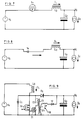
- FIGS 3 to 8 illustrate the operation of the apparatus represented in Figure 2.
- Figures 9, 10 and 11 illustrate the application of the invention to three other typical exemplary converters.
- Such a regulator comprises a pulse width modulated (PWM) power switch S1 that controls the magnitude of the current flowing through the inductor Lo according to the required output voltage Vo across the output port or according to the required output current Io.
- Switch S1 is shown by way of example by a transistor fed by a voltage source Vs connected across the input port of the apparatus.
- the unidirectional switch D1 e.g. a diode
- Power switch S1 is turned ON or OFF in response to control pulses applied to its control electrode or gate.
- Switch S1 has finite turn-off and turn-on times and diode D1 causes a reverse recovery current to flow through it when turned OFF.
- the result of these non-ideal conditions during the switching transitions of switch S1 is that the current through it and the voltage across it exist simultaneously, which causes a loss in the switch. This switching loss is proportional to the frequency and is thus a major limitation to high frequency operation.
- the exemplary circuit described herein above is modified according to the invention as shown in Figure 2.
- the modification consists in connecting a low power switching DC-to-DC converter 10 in parallel arrangement with the controlled power switch S1 so that it is allowed to operate from the input voltage and transfer energy from input to output during the switching periods of the controlled power switch S1.
- the purpose of the switching converter 10 is to set the voltage across the power switch S1 to be near to zero during its turn-on (rise of current) and turn-off (fall of current) periods, thereby significantly reducing the switching loss.
- the switching converter 10 comprises a transformer 13, the primary winding 13P of which is arranged in series connection with a controlled switching device 11 (here shown as a transistor) across the input voltage Vs.
- the secondary winding 13S of transformer 13 is arranged in series connection with a unidirectional switch 12 (here shown as a diode).
- a capacitor 14 connected across power switch S1.
- FIG. 3 shows typical waveforms in the arrangement of Figure 2 and Figures 4 to 8 show the current paths being set in the arrangement during five successive time periods.
- main switch S1 is OFF and the inductor current ID1 is flowing through diode D1.
- switch 11 is turned ON at time to.
- a current Iws flows through the secondary winding of transformer 13 and through diode 12. Because of the equivalent inductance Le of transformer 13, that current builds up in a linear way starting from zero at a rate of nVs/Le (where n is the ratio of numbers of secondary to primary turns of 13) until it equals the value IL of the current flowing in the inductance Lo at time t1.
- the secondary winding of transformer 13 provides all the current IL, the current through diode D1 becomes zero and D1 turns OFF, thereby allowing the voltage VD1 across its terminals to rise. Since the current Iws builds up at a controlled rate, the turn-off of diode D1 is made soft, i.e. the reverse recovery current is near to zero. Because switch 11 is still ON, the current Iws continues to flow and the voltage across capacitor 14 decreases to zero at time t2. The discharge of 14 is sinuso ⁇ dal in nature due to the resonance of 14 and Le. At time t2, if the current Iws is still greater than IL, the excess current will try to raise the voltage but this cannot happen because the anti-parallel intrinsic diode of switch S1 clamps this voltage to the input voltage Vs.
- this switch can be turned ON with a very low switching loss.
- the current Iws falls to zero and at time t3, switch 11 is turned OFF with only a small current through it. Since both the turn-on and turn-off of switch 11 occur with low values of conducted current its switching loss can be made very low.
- the sum of the currents Iws and Is1 equals the instantaneous value of current IL, the current Is1 through switch S1 builds up from zero at a rate equal to the fall of current Iws.
- switch S1 is turned OFF.
- the current IL is then provided by capacitor 14.
- the voltage Vs1 across the switch S1 falls from the value Vs to zero at time t5 when diode D1 turns ON.
- capacitor 14 provides most of the current IL, so that the loss during the turn-off of S1 is kept very low.
- the power switch S1 should be allowed to switch only when the voltage across it is near to zero, which happens if the voltage across diode D1 equals the value of the input voltage Vs.
- the switch S1 is thus controlled by suitable control means 15 arranged to generate a control pulse in response to an enabling pulse EN.
- Said enable pulse is produced by a voltage sense device 16 connected for measuring the voltage VD1 across diode D1 and for producing said enabling pulse when the voltage VD1 has reached the input voltage value Vs.
- Figure 3 shows that switch 11 is turned ON first and when the voltage across main switch S1 is near to zero, switch S1 is allowed to turn ON in a lossless way.
- An advantage in using a switching current converter according to the invention resides in that all the power of the converter is being coupled from the input to the output, thereby to result in achieving a high total efficiency.
- the current converter provides protection of the voltage source Vs automatically in case of failure of diode D1.
- the output voltage VD1 is zero and the voltage sense device 16 inhibits switch S1 to turn ON as explained hereabove.
- no short circuit of the supply voltage Vs can occur as it happens in the prior art arrangements, wherein it is the usual practice to arrange two redundant diodes D1 in series for more failure tolerant operation. Deleting the extra diode, in accordance with this invention, also provides an increase in efficiency.
- Figure 9 shows the circuit of a typical boost converter comprising the invention.
- the switching converter 10 therein operates in a similar way to that for the buck converter of Figure 2 except that now it is the input current of converter 10 that forces the voltage across main switch S1 to be zero just before it is turned ON.
- the waveforms are similar to those shown in Figure 3.
- Figure 10 shows the circuit of a typical forward converter comprising the invention.
- Figure 11 shows the typical circuit (known per se) of a PWM push-pull converter comprising the invention.
- This arrangement comprises a transformer T2 and two power switches S1 and S1'.
- each power switch there is arranged a switching converter 10, 10' as shown in Figure 9.
- Each active switching converter controls the corresponding power switch as described hereabove and serves as a stress relieving means for that power switch.
Landscapes
- Engineering & Computer Science (AREA)
- Power Engineering (AREA)
- Dc-Dc Converters (AREA)
- Inverter Devices (AREA)
Claims (3)
- Procédé pour réduire les pertes de commutation dans au moins un commutateur de puissance commandé (S1) connecté dans un circuit électrique ayant une entrée connectée aux bornes d'une source de tension d'entrée et ayant une sortie, caractérisé par le fait que l'on connecte un convertisseur à commutation (10) en parallèle avec chaque commutateur de puissance (S1) entre la source et le drain, de manière qu'il travaille sous la tension d'entrée et transfère l'énergie de l'entrée vers la sortie pendant les temps de commutation dans l'état conducteur du commutateur de puissance commandé et de manière que chaque commutateur de puissance commute dans son état conducteur lorsqu'une tension pratiquement nulle est présente à ses bornes.
- Procédé selon la revendication 1, caractérisé en ce que l'étape de connexion du convertisseur à commutation comprend la connexion d'un transformateur (13) ayant un enroulement primaire (13P) et un enroulement secondaire (13S), ledit enroulement primaire (WP) étant connecté en série avec un premier dispositif de commutation commandé (11) sur la tension d'entrée, ledit enroulement secondaire étant connecté en série avec un second dispositif de commutation unidirectionnel (12) sur la tension de sortie commandée,la connexion d'un condensateur (14) en parallèle avec un commutateur de puissance commandé (S1) correspondant, etla commande dudit commutateur de puissance commandé (S1) afin de l'amener dans son état conducteur uniquement après que ledit premier dispositif de commutation (11) soit rendu conducteur, de manière que le commutateur de puissance commandé (S1) commute dans son état conducteur avec une tension pratiquement nulle à ses bornes.
- Procédé selon la revendication 1, caractérisé en ce que l'étape de connexion du convertisseur à commutation comprend la connexion d'un transformateur (13) ayant un enroulement primaire (13P) et un enroulement secondaire (13S), ledit enroulement primaire étant connecté en série avec un premier dispositif de commutation commandé (11) aux bornes du commutateur de puissance commandé (S1), ledit enroulement secondaire étant connecté en série avec un second dispositif de commutation unidirectionnel (12) sur la tension de sortie,la connexion d'un condensateur (14) en parallèle avec le commutateur de puissance commandé (S1) correspondant, etla commande dudit commutateur de puissance afin de l'amener dans son état conducteur uniquement après que ledit premier dispositif de commutation soit rendu conducteur, de manière que le commutateur de puissance (S1) commute dans son état conducteur avec une tension pratiquement nulle à ses bornes.
Applications Claiming Priority (2)
| Application Number | Priority Date | Filing Date | Title |
|---|---|---|---|
| FR9100669A FR2671922B1 (fr) | 1991-01-22 | 1991-01-22 | Procede pour reduire les pertes de commutation creees par un commutateur de puissance. |
| FR9100669 | 1991-01-22 |
Publications (3)
| Publication Number | Publication Date |
|---|---|
| EP0496718A2 EP0496718A2 (fr) | 1992-07-29 |
| EP0496718A3 EP0496718A3 (en) | 1992-10-28 |
| EP0496718B1 true EP0496718B1 (fr) | 1996-03-13 |
Family
ID=9408913
Family Applications (1)
| Application Number | Title | Priority Date | Filing Date |
|---|---|---|---|
| EP92870011A Expired - Lifetime EP0496718B1 (fr) | 1991-01-22 | 1992-01-17 | Méthode pour minimiser les pertes de commutation dans un commutateur de puissance |
Country Status (6)
| Country | Link |
|---|---|
| US (1) | US5293111A (fr) |
| EP (1) | EP0496718B1 (fr) |
| JP (1) | JPH0549251A (fr) |
| CA (1) | CA2059457C (fr) |
| DE (1) | DE69208902D1 (fr) |
| FR (1) | FR2671922B1 (fr) |
Families Citing this family (22)
| Publication number | Priority date | Publication date | Assignee | Title |
|---|---|---|---|---|
| US5307005A (en) * | 1992-12-23 | 1994-04-26 | International Business Machines Corporation | Zero current switching reverse recovery circuit |
| US5416403A (en) * | 1993-02-11 | 1995-05-16 | Hewlett-Packard Corporation | Current stabilizing circuit |
| US5388040A (en) * | 1993-09-30 | 1995-02-07 | Hughes Aircraft Company | Series resonant converter having an actively controlled third element |
| US5457379A (en) * | 1993-10-15 | 1995-10-10 | At&T Ipm Corp. | High efficiency switch mode regulator |
| US5461302A (en) * | 1993-11-30 | 1995-10-24 | At&T Corp. | Modulated snubber driver for active snubber network |
| US5543704A (en) * | 1994-06-08 | 1996-08-06 | Telefonaktiebolaget Lm Ericsson | Pulse width modulated DC-to-DC boost converter |
| US5610804A (en) * | 1994-06-20 | 1997-03-11 | Tdk Corporation | Power supply with dual energy transfer circuits for power factor correction |
| US5636114A (en) * | 1995-11-30 | 1997-06-03 | Electronic Measurements, Inc. | Lossless snubber circuit for use in power converters |
| US5877610A (en) * | 1997-10-06 | 1999-03-02 | Northrop Grumman Corporation | Multiple cell boost converter |
| CA2220747A1 (fr) * | 1997-11-10 | 1999-05-10 | Praveen Kumar Jain | Convertisseurs c.c.-c.c. |
| US5959438A (en) * | 1998-01-09 | 1999-09-28 | Delta Electronics, Inc. | Soft-switched boost converter with isolated active snubber |
| US6069803A (en) * | 1999-02-12 | 2000-05-30 | Astec International Limited | Offset resonance zero volt switching flyback converter |
| US6211792B1 (en) | 1999-08-13 | 2001-04-03 | JADRIć IVAN | Method and apparatus detecting a failed thyristor |
| US6404265B1 (en) | 1999-08-13 | 2002-06-11 | York International Corporation | Highly efficient driver circuit for a solid state switch |
| US6404346B1 (en) | 1999-08-13 | 2002-06-11 | York International Corporation | Method and apparatus for detecting a failed thyristor |
| US6341076B1 (en) | 2000-05-23 | 2002-01-22 | Next Power Corporation | Loss reduction circuit for switching power converters |
| US6236191B1 (en) | 2000-06-02 | 2001-05-22 | Astec International Limited | Zero voltage switching boost topology |
| US6434029B1 (en) | 2001-10-17 | 2002-08-13 | Astec International Limited | Boost topology having an auxiliary winding on the snubber inductor |
| US6987675B2 (en) * | 2003-05-23 | 2006-01-17 | Delta Electronics, Inc. | Soft-switched power converters |
| EP1635462A1 (fr) * | 2004-09-13 | 2006-03-15 | Peter Laurence Hutchins | Convertisseur de puissance à découpage à haute efficacité |
| US8644037B2 (en) * | 2008-07-15 | 2014-02-04 | General Electric Company | AC-AC converter with high frequency link |
| JP7313904B2 (ja) * | 2019-05-24 | 2023-07-25 | 株式会社日立製作所 | 冗長化定電流電源及びセンサシステム |
Citations (1)
| Publication number | Priority date | Publication date | Assignee | Title |
|---|---|---|---|---|
| EP0334100A2 (fr) * | 1988-03-21 | 1989-09-27 | International Business Machines Corporation | Circuit de commutation en pont complet |
Family Cites Families (10)
| Publication number | Priority date | Publication date | Assignee | Title |
|---|---|---|---|---|
| GB1529679A (en) * | 1974-12-21 | 1978-10-25 | Simms Group Res Dev Ltd | Dc supply circuits |
| DE3007597C2 (de) * | 1980-02-28 | 1982-04-15 | Siemens Ag, 1000 Berlin Und 8000 Muenchen | Schutzbeschaltungsanordnung für Halbleiterschalter |
| FR2550399B1 (fr) * | 1983-08-05 | 1989-07-07 | Cem Comp Electro Mec | Dispositif d'aide a la commutation |
| US4675796A (en) * | 1985-05-17 | 1987-06-23 | Veeco Instruments, Inc. | High switching frequency converter auxiliary magnetic winding and snubber circuit |
| US4725768A (en) * | 1985-11-12 | 1988-02-16 | Toko Kabushiki Kaisha | Switching regulated power supply employing an elongated metallic conductive inductor having a magnetic thin film coating |
| US4857822A (en) * | 1987-09-23 | 1989-08-15 | Virginia Tech Intellectual Properties, Inc. | Zero-voltage-switched multi-resonant converters including the buck and forward type |
| US4814963A (en) * | 1987-09-30 | 1989-03-21 | Spectra Physics | Modular power supply with variable input voltage and output voltage flyback power modules |
| JPH0734653B2 (ja) * | 1989-09-05 | 1995-04-12 | 九州大学長 | 電源装置 |
| US4959764A (en) * | 1989-11-14 | 1990-09-25 | Computer Products, Inc. | DC/DC converter switching at zero voltage |
| US5008795A (en) * | 1990-03-23 | 1991-04-16 | Unisys Corporation | Switched capacitor interleaved forward power converter |
-
1991
- 1991-01-22 FR FR9100669A patent/FR2671922B1/fr not_active Expired - Fee Related
-
1992
- 1992-01-16 CA CA002059457A patent/CA2059457C/fr not_active Expired - Fee Related
- 1992-01-17 EP EP92870011A patent/EP0496718B1/fr not_active Expired - Lifetime
- 1992-01-17 DE DE69208902T patent/DE69208902D1/de not_active Expired - Lifetime
- 1992-01-22 US US07/823,752 patent/US5293111A/en not_active Expired - Fee Related
- 1992-01-22 JP JP4009107A patent/JPH0549251A/ja active Pending
Patent Citations (1)
| Publication number | Priority date | Publication date | Assignee | Title |
|---|---|---|---|---|
| EP0334100A2 (fr) * | 1988-03-21 | 1989-09-27 | International Business Machines Corporation | Circuit de commutation en pont complet |
Also Published As
| Publication number | Publication date |
|---|---|
| FR2671922A1 (fr) | 1992-07-24 |
| CA2059457A1 (fr) | 1992-07-23 |
| DE69208902D1 (de) | 1996-04-18 |
| US5293111A (en) | 1994-03-08 |
| FR2671922B1 (fr) | 1994-02-11 |
| CA2059457C (fr) | 2001-10-23 |
| EP0496718A2 (fr) | 1992-07-29 |
| JPH0549251A (ja) | 1993-02-26 |
| EP0496718A3 (en) | 1992-10-28 |
Similar Documents
| Publication | Publication Date | Title |
|---|---|---|
| EP0496718B1 (fr) | Méthode pour minimiser les pertes de commutation dans un commutateur de puissance | |
| US6188592B1 (en) | Externally-driven scheme for synchronous rectification | |
| US6038148A (en) | Self-driven synchronous rectification scheme | |
| US5781419A (en) | Soft switching DC-to-DC converter with coupled inductors | |
| KR100519440B1 (ko) | 소프트펄스폭변조스위칭을이용한위상스태거방식의풀-브리지변환기 | |
| US6256214B1 (en) | General self-driven synchronous rectification scheme for synchronous rectifiers having a floating gate | |
| US5543704A (en) | Pulse width modulated DC-to-DC boost converter | |
| EP0602835B1 (fr) | Circuits de commande de tension | |
| US5434768A (en) | Fixed frequency converter switching at zero voltage | |
| US5471376A (en) | Low-loss active voltage-clamp circuit for single-ended forward PWM converter | |
| CN100511942C (zh) | 正反激双向dc-dc变换器的控制方法 | |
| US6583993B2 (en) | Self-driven synchronous rectification scheme for wide output range | |
| EP0741447A2 (fr) | Circuit et méthode pour le contrÔle d'un convertisseur avec redresseur synchrone | |
| US5307005A (en) | Zero current switching reverse recovery circuit | |
| US6560127B2 (en) | Power conversion circuit having improved zero voltage switching | |
| JPH0760998B2 (ja) | 全ブリッジ・電力変換回路 | |
| US20020136033A1 (en) | Switching power supply | |
| KR20020074203A (ko) | 플라이백 컨버터를 위한 누설에너지 회복 시스템과누설에너지 회복 방법 | |
| US5457379A (en) | High efficiency switch mode regulator | |
| US5986904A (en) | Self-regulating lossless snubber circuit | |
| US5831838A (en) | Resonant fly-forward converter circuit | |
| JP3259128B2 (ja) | 同期整流回路 | |
| US4974142A (en) | Bootstrap drive for a switch-mode power converter | |
| Lindroth et al. | Methods of improving efficiency in wide input range boost converters at low input voltages | |
| KR100204495B1 (ko) | 영전압스위칭 직류-직류 강압형 컨버터 |
Legal Events
| Date | Code | Title | Description |
|---|---|---|---|
| PUAI | Public reference made under article 153(3) epc to a published international application that has entered the european phase |
Free format text: ORIGINAL CODE: 0009012 |
|
| AK | Designated contracting states |
Kind code of ref document: A2 Designated state(s): BE DE DK ES FR GB IT |
|
| PUAL | Search report despatched |
Free format text: ORIGINAL CODE: 0009013 |
|
| AK | Designated contracting states |
Kind code of ref document: A3 Designated state(s): BE DE DK ES FR GB IT |
|
| 17P | Request for examination filed |
Effective date: 19930121 |
|
| 17Q | First examination report despatched |
Effective date: 19940905 |
|
| GRAA | (expected) grant |
Free format text: ORIGINAL CODE: 0009210 |
|
| AK | Designated contracting states |
Kind code of ref document: B1 Designated state(s): BE DE DK ES FR GB IT |
|
| PG25 | Lapsed in a contracting state [announced via postgrant information from national office to epo] |
Ref country code: FR Effective date: 19960313 Ref country code: ES Free format text: THE PATENT HAS BEEN ANNULLED BY A DECISION OF A NATIONAL AUTHORITY Effective date: 19960313 Ref country code: DK Effective date: 19960313 Ref country code: BE Effective date: 19960313 |
|
| REF | Corresponds to: |
Ref document number: 69208902 Country of ref document: DE Date of ref document: 19960418 |
|
| ITF | It: translation for a ep patent filed | ||
| PG25 | Lapsed in a contracting state [announced via postgrant information from national office to epo] |
Ref country code: DE Effective date: 19960614 |
|
| EN | Fr: translation not filed | ||
| PLBE | No opposition filed within time limit |
Free format text: ORIGINAL CODE: 0009261 |
|
| 26N | No opposition filed | ||
| PGFP | Annual fee paid to national office [announced via postgrant information from national office to epo] |
Ref country code: GB Payment date: 19991224 Year of fee payment: 9 |
|
| PG25 | Lapsed in a contracting state [announced via postgrant information from national office to epo] |
Ref country code: GB Free format text: LAPSE BECAUSE OF NON-PAYMENT OF DUE FEES Effective date: 20010117 |
|
| GBPC | Gb: european patent ceased through non-payment of renewal fee |
Effective date: 20010117 |
|
| PG25 | Lapsed in a contracting state [announced via postgrant information from national office to epo] |
Ref country code: IT Free format text: LAPSE BECAUSE OF NON-PAYMENT OF DUE FEES Effective date: 20050117 |