EP0497432A1 - Apparat zum Betrieb einer Halbleiterlaservorrichtung - Google Patents
Apparat zum Betrieb einer Halbleiterlaservorrichtung Download PDFInfo
- Publication number
- EP0497432A1 EP0497432A1 EP92201061A EP92201061A EP0497432A1 EP 0497432 A1 EP0497432 A1 EP 0497432A1 EP 92201061 A EP92201061 A EP 92201061A EP 92201061 A EP92201061 A EP 92201061A EP 0497432 A1 EP0497432 A1 EP 0497432A1
- Authority
- EP
- European Patent Office
- Prior art keywords
- optical output
- signal
- output
- laser device
- driving
- Prior art date
- Legal status (The legal status is an assumption and is not a legal conclusion. Google has not performed a legal analysis and makes no representation as to the accuracy of the status listed.)
- Granted
Links
- 239000004065 semiconductor Substances 0.000 title claims abstract description 22
- 230000003287 optical effect Effects 0.000 claims abstract description 72
- 230000004044 response Effects 0.000 claims abstract description 13
- 238000012544 monitoring process Methods 0.000 claims abstract description 8
- 238000010586 diagram Methods 0.000 description 6
- 238000013139 quantization Methods 0.000 description 6
- 239000003990 capacitor Substances 0.000 description 4
- 230000008859 change Effects 0.000 description 3
- 238000004891 communication Methods 0.000 description 1
- 230000001276 controlling effect Effects 0.000 description 1
- 238000000034 method Methods 0.000 description 1
- 238000012986 modification Methods 0.000 description 1
- 230000004048 modification Effects 0.000 description 1
- 230000010355 oscillation Effects 0.000 description 1
- 230000001105 regulatory effect Effects 0.000 description 1
Images


Classifications
-
- H—ELECTRICITY
- H01—ELECTRIC ELEMENTS
- H01S—DEVICES USING THE PROCESS OF LIGHT AMPLIFICATION BY STIMULATED EMISSION OF RADIATION [LASER] TO AMPLIFY OR GENERATE LIGHT; DEVICES USING STIMULATED EMISSION OF ELECTROMAGNETIC RADIATION IN WAVE RANGES OTHER THAN OPTICAL
- H01S5/00—Semiconductor lasers
- H01S5/06—Arrangements for controlling the laser output parameters, e.g. by operating on the active medium
- H01S5/062—Arrangements for controlling the laser output parameters, e.g. by operating on the active medium by varying the potential of the electrodes
- H01S5/06209—Arrangements for controlling the laser output parameters, e.g. by operating on the active medium by varying the potential of the electrodes in single-section lasers
-
- H—ELECTRICITY
- H01—ELECTRIC ELEMENTS
- H01S—DEVICES USING THE PROCESS OF LIGHT AMPLIFICATION BY STIMULATED EMISSION OF RADIATION [LASER] TO AMPLIFY OR GENERATE LIGHT; DEVICES USING STIMULATED EMISSION OF ELECTROMAGNETIC RADIATION IN WAVE RANGES OTHER THAN OPTICAL
- H01S5/00—Semiconductor lasers
- H01S5/06—Arrangements for controlling the laser output parameters, e.g. by operating on the active medium
- H01S5/068—Stabilisation of laser output parameters
- H01S5/0683—Stabilisation of laser output parameters by monitoring the optical output parameters
-
- H—ELECTRICITY
- H05—ELECTRIC TECHNIQUES NOT OTHERWISE PROVIDED FOR
- H05B—ELECTRIC HEATING; ELECTRIC LIGHT SOURCES NOT OTHERWISE PROVIDED FOR; CIRCUIT ARRANGEMENTS FOR ELECTRIC LIGHT SOURCES, IN GENERAL
- H05B45/00—Circuit arrangements for operating light-emitting diodes [LED]
- H05B45/10—Controlling the intensity of the light
- H05B45/14—Controlling the intensity of the light using electrical feedback from LEDs or from LED modules
-
- H—ELECTRICITY
- H01—ELECTRIC ELEMENTS
- H01S—DEVICES USING THE PROCESS OF LIGHT AMPLIFICATION BY STIMULATED EMISSION OF RADIATION [LASER] TO AMPLIFY OR GENERATE LIGHT; DEVICES USING STIMULATED EMISSION OF ELECTROMAGNETIC RADIATION IN WAVE RANGES OTHER THAN OPTICAL
- H01S5/00—Semiconductor lasers
- H01S5/04—Processes or apparatus for excitation, e.g. pumping, e.g. by electron beams
- H01S5/042—Electrical excitation ; Circuits therefor
-
- H—ELECTRICITY
- H01—ELECTRIC ELEMENTS
- H01S—DEVICES USING THE PROCESS OF LIGHT AMPLIFICATION BY STIMULATED EMISSION OF RADIATION [LASER] TO AMPLIFY OR GENERATE LIGHT; DEVICES USING STIMULATED EMISSION OF ELECTROMAGNETIC RADIATION IN WAVE RANGES OTHER THAN OPTICAL
- H01S5/00—Semiconductor lasers
- H01S5/06—Arrangements for controlling the laser output parameters, e.g. by operating on the active medium
- H01S5/0617—Arrangements for controlling the laser output parameters, e.g. by operating on the active medium using memorised or pre-programmed laser characteristics
Definitions
- This invention relates to a method of driving a semiconductor laser device and an apparatus for driving a semiconductor laser device.
- a forward current I F is supplied to a pn junction in the laser device.
- the relationship between the forward current I F and the optical output P O of a semiconductor laser device is not linear.
- the laser device begins to oscillate a laser beam at a certain level of the current (a threshold current I th ).
- a threshold current I th As the forward current I F increases further, the laser output P O also increases.
- Figure 1 shows an example of the relationship between the forward current I F and the optical output P O of a semiconductor laser device.
- the level of a threshold current I th and the rate of change in an optical output P O with respect to the changes in a forward current I F are not constant but vary according to an ambient temperature or to the individual semiconductor laser device. Such a rate of change in an optical output P O is called a differential efficiency ⁇ .
- a semiconductor laser diode When a semiconductor laser diode is driven at an optical output of a constant level, the system shown in Fig. 2 is generally used.
- a semiconductor laser diode 1 is driven by a current source 4 which is controlled by the output of an amplifier 3 .
- the optical output of the laser diode 1 is monitored by a photodiode 2 , and is converted into voltage by a resistor 5 .
- the voltage is applied to one input terminal of the amplifier 3 .
- the system shown in Fig. 2 constitutes a negative feedback loop.
- a reference voltage V ref is applied to the other input terminal of the amplifier 3 so that the optical output of the laser diode 1 is controlled to have a predetermined level corresponding to the reference voltage V ref .
- FIG. 2 The system shown in Fig. 2 is used for obtaining a constant optical output of a predetermined level.
- a semiconductor laser diode such as laser printers or optical communication
- a semiconductor laser diode producing a constant optical output of a predetermined level is turned on and off at a high speed.
- Figure 3 shows an example of a system used for such an application.
- the system of Fig. 3 comprises, in addition to the components in the system of Fig. 2, an analog switch 7 and a capacitor 8 which constitute a sample-hold circuit.
- the system of Fig. 3 further comprises a high-speed switch 6 and a buffer amplifier 9 .
- the operation of the system of Fig. 3 will be described. First, the switch 6 is set to the right position, and the switch 7 is turned on to obtain an optical output of a predetermined level corresponding to the reference voltage V ref . Thereafter, the switch 7 is turned off. At this stage, the voltage applied to the amplifier 9 is held at the voltage level of the capacitor 8 so that the driving current supplied to the laser diode 1 is maintained to be constant. Then, the switch 6 is turned off and on at a high speed, resulting in a high-speed switching of the optical output of a constant level.
- the system of Fig. 4 is not provided with the sample-hold circuit (the analog switch 7 and capacitor 8 ) and the buffer amplifier 9 which are used in the system of Fig. 3, but comprises an up/down counter 11 , a D/A converter 10, and an oscillator 12.
- the amplifier 3 functions as a comparator. When the output of the comparator 3 is "HIGH”, the up/down counter 11 counts up the output pulses of the oscillator 12. When the output of the comparator 3 is "LOW”, in contrast, the counter 11 counts down the output pulses of the oscillator 12. The output of the counter 11 is converted into an analog value corresponding to the forward current I F by the D/A converter 10.
- the forward current I F from the current source 4 is supplied to the semiconductor laser diode 1 to drive the laser diode 1.
- the system of Fig. 4 constitutes a negative feedback loop so that the optical output of the laser diode 1 is regulated at a constant value corresponding to the reference voltage V ref .
- An error which corresponds to one pulse of the output of the oscillator 12 may occur in the level of the optical output.
- I F -P O characeristics of a semiconductor laser diode are such that, if a foward current I F is less than the threshold current I th , laser oscillation does not occur. Accordingly, if the forward current I F is less than the threshold current I th , it cannot be used for control in driving the laser diode. For this reason, the quantization error of the optical output P O is greater than the quantization error of the forward current I F , resulting in less accuracy in controlling the optical output P O .
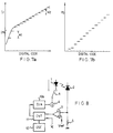
- Figure 5 (a) shows a relation between an input (digital codes) and an output (forward current I F) of D/A converter which are usually used in a conventional system such as shown in Fig. 4.
- Figure 5 (b) shows a relation between optical outputs P O of laser diode and digital codes in the conventional system of Fig. 4 which employs a D/A converter having the linear characteristics shown in Fig. 5 (a).
- the digital codes corresponding to values lower than the threshold current I th of a laser diode do not contribute to the optical output of the laser diode. As shown in Fig. 5 (b), therefore, the range of the codes which are effective in practical use is restricted, resulting in a reduced effective resolution of the D/A converter 10.
- "W q " indicates a quantization width of the optical output P O .
- an apparatus for driving a semiconductor laser device to develop a predetermined constant optical output comprising means for monitoring an optical output of the laser device and generating a signal which is representative of the optical output and a feedback loop comprising:- comparing means for comparing said signal representative of the optical output with a reference value and providing an output signal, said output signal depending on a comparison of said signal representative of the optical output with said reference value; counting means for developing a digital signal for said output signal being provided from said comparing means; D/A converting means for developing a control signal in response to said digital signal; and current supply means for driving the laser device at said predetermined optical output in response to said first control signal; said apparatus being characterised in that said D/A converting means has a non-linear characteristic.
- an apparatus for driving a semiconductor laser device to develop a predetermined constant optical output comprising means for monitoring an optical output of the laser device and generating a signal which is representative of the optical output and a feedback loop comprising:- comparing means for comparing said signal representative of the optical output with a reference value and providing an output signal, said output signal depending on a comparison of said signal representative of the optical output with said reference value; counting means for developing a digital signal for said output signal being provided from said comparing means; D/A converting means for developing a control signal in response to said digital signal; and current supply means for driving the laser device at said predetermined optical output in response to said first control signal; said apparatus being characterised in that said D/A converting means provides an offset output.
- the invention described herein makes possible the objectives of (1) providing an apparatus for driving a semiconductor laser device which can control an optical output level with high accuracy; and (2) providing an apparatus for driving a semiconductor laser diode which can change the optical output to desired levels at a very high frequency.
- Figure 6 shows an embodiment of the invention.
- the configuration of the system shown in Fig. 6 is similar to that of the system of Fig. 4, but employs a D/A converter 10a having non-linear characteristics instead of the converter 10 in the system of Fig. 4.
- the relation between an input (digital codes) and an output (forward current I F ) of the D/A converter 10a in this embodiment is shown in Fig. 7(a).
- the quantization width W1 is wide
- the quantization width W2 is narrow.
- Figure 7 (b) shows a relation between optical output P O and the digital codes of the D/A converter 10a in this embodiment. Because of the non-linear characteristics of the converter 10a, the number of the digital codes which correspond to the current levels lower than the threshold current I th is small, compared to that of the conventional system which is shown in Fig. 5. In other words, the number of the codes which are effective in the control of the optical output of the laser diode is large even when the D/A converter 10a has the same number of digital codes as that of the D/A converter 10 of Fig. 4, resulting in an improved effective resolution of the D/A converter 10a and also in a very accurate control of the optical output.
- Figure 8 shows a further embodiment of the invention.
- the configuration of the system shown in Fig. 8 is similar to that of the system of Fig. 6, but employs a D/A converter 10b having a characteristic that an offset current of a certain level flows when the digital code is zero.
- the offset current I OS is greater than the threshold current I th .
- the offset current I OS is smaller than the threshold current I th .
- the relation between an input (digital code) and an output (forward current I F ) of the D/A converter 10b having the characteristics of Fig. 9 (a) is shown in Fig. 9 (c), and that of the D/A converter 10b having the characteristics of Fig.
- Figure 10 shows a further embodiment of the invention.
- the configuration of the system shown in Fig. 10 is similar to that of the system of Fig. 4 except that a second current source 4a is provided.
- the current source 4a supplies an offset current I OS of a certain level to the laser diode 1 , i.e., the laser diode 1 is driven by the sum of the forward current I F and the offset current I OS .
- Figures 11 (a) and 11 (b) show the relations between digital codes of the D/A converter 10 and optical outputs P O of the laser diode 1 when the offset current I OS is greater or smaller than the threshold current I th , respectively.
- the offset current I OS When the offset current I OS is smaller than the threshold current I th , the number of the codes which are ineffective in the control of the optical output of the laser diode 1 is small (Fig. 11 (b)).
- the offset current I OS is greater than the threshold current I th , there is no code which is ineffective in the control of the optical output of the laser diode 1 (Fig. 11(a)). Consequently, the quantization widths W3 (Fig. 11 (a)) or W4 (Fig. 11(b)) in the system of Fig. 10 is narrow, compared to those obtained by the system of Fig. 4 even when the D/A converters 10 used in both the systems have the same resolution characteristics, resulting in an improved effective resolution of the D/A converter 10 and also in a very accurate control of the optical output.
- a D/A converter having low resolution which can be easily produced at a low cost can be used in an apparatus of the present invention. Therefore, an apparatus of the present invention can be easily manufactured a low cost and is easily integrated.
Landscapes
- Physics & Mathematics (AREA)
- Condensed Matter Physics & Semiconductors (AREA)
- General Physics & Mathematics (AREA)
- Electromagnetism (AREA)
- Optics & Photonics (AREA)
- Semiconductor Lasers (AREA)
Applications Claiming Priority (15)
| Application Number | Priority Date | Filing Date | Title |
|---|---|---|---|
| JP9017187 | 1987-04-13 | ||
| JP90170/87 | 1987-04-13 | ||
| JP90168/87 | 1987-04-13 | ||
| JP62090172A JPS63254781A (ja) | 1987-04-13 | 1987-04-13 | 半導体レ−ザ駆動方式 |
| JP90171/87 | 1987-04-13 | ||
| JP62090168A JPS63254778A (ja) | 1987-04-13 | 1987-04-13 | 半導体レ−ザ駆動方式 |
| JP90169/87 | 1987-04-13 | ||
| JP62090169A JPS63254779A (ja) | 1987-04-13 | 1987-04-13 | 半導体レ−ザ駆動方式 |
| JP90172/87 | 1987-04-13 | ||
| JP62090170A JPS63254780A (ja) | 1987-04-13 | 1987-04-13 | 半導体レ−ザ駆動方式 |
| JP2588688 | 1988-02-05 | ||
| JP25886/88 | 1988-02-05 | ||
| JP63055747A JPH067614B2 (ja) | 1987-04-13 | 1988-03-09 | 半導体レーザ駆動方式 |
| JP55747/88 | 1988-03-09 | ||
| EP88303348A EP0287360B1 (de) | 1987-04-13 | 1988-04-13 | Ansteuerungsvorrichtung für einen Halbleiterlaser |
Related Parent Applications (1)
| Application Number | Title | Priority Date | Filing Date |
|---|---|---|---|
| EP88303348.2 Division | 1988-04-13 |
Publications (2)
| Publication Number | Publication Date |
|---|---|
| EP0497432A1 true EP0497432A1 (de) | 1992-08-05 |
| EP0497432B1 EP0497432B1 (de) | 1995-07-19 |
Family
ID=27564080
Family Applications (3)
| Application Number | Title | Priority Date | Filing Date |
|---|---|---|---|
| EP88303348A Expired - Lifetime EP0287360B1 (de) | 1987-04-13 | 1988-04-13 | Ansteuerungsvorrichtung für einen Halbleiterlaser |
| EP92201060A Expired - Lifetime EP0497431B1 (de) | 1987-04-13 | 1988-04-13 | Apparat zum Betreiben einer Halbleiterlaservorrichtung |
| EP92201061A Expired - Lifetime EP0497432B1 (de) | 1987-04-13 | 1988-04-13 | Apparat zum Betrieb einer Halbleiterlaservorrichtung |
Family Applications Before (2)
| Application Number | Title | Priority Date | Filing Date |
|---|---|---|---|
| EP88303348A Expired - Lifetime EP0287360B1 (de) | 1987-04-13 | 1988-04-13 | Ansteuerungsvorrichtung für einen Halbleiterlaser |
| EP92201060A Expired - Lifetime EP0497431B1 (de) | 1987-04-13 | 1988-04-13 | Apparat zum Betreiben einer Halbleiterlaservorrichtung |
Country Status (3)
| Country | Link |
|---|---|
| US (1) | US4912714A (de) |
| EP (3) | EP0287360B1 (de) |
| DE (3) | DE3879250T2 (de) |
Cited By (2)
| Publication number | Priority date | Publication date | Assignee | Title |
|---|---|---|---|---|
| GB2291511A (en) * | 1994-07-18 | 1996-01-24 | Martin Lawrence | A method of stabilising the output intensity and or output frequency of an optical light source using an electronic counting technique |
| EP1136992A2 (de) * | 2000-03-24 | 2001-09-26 | Samsung Electronics Co., Ltd. | Vorrichtung und Verfahren zur automatischen Steuerung der Laserdiodenleistung |
Families Citing this family (28)
| Publication number | Priority date | Publication date | Assignee | Title |
|---|---|---|---|---|
| JPH03202808A (ja) * | 1989-12-28 | 1991-09-04 | Toshiba Corp | レーザ発振器の光量制御装置 |
| US5111065A (en) * | 1990-03-23 | 1992-05-05 | Massachusetts Institute Of Technology | Diode driver circuit utilizing discrete-value DC current source |
| US5068863A (en) * | 1990-04-17 | 1991-11-26 | Wavelengths Lasers, Inc. | Compensating circuit for high power lasers |
| JP2645177B2 (ja) * | 1990-10-17 | 1997-08-25 | 株式会社テック | レーザパワー制御装置 |
| US5222072A (en) * | 1990-10-17 | 1993-06-22 | Tokyo Electric Co., Ltd. | Laser power control apparatus |
| JP2546080B2 (ja) * | 1991-05-10 | 1996-10-23 | 富士通株式会社 | 半導体レーザー制御装置 |
| JPH0590691A (ja) * | 1991-09-26 | 1993-04-09 | Sharp Corp | レーザ光出力制御装置 |
| JP2917642B2 (ja) * | 1992-01-24 | 1999-07-12 | 三菱電機株式会社 | レーザ出力制御装置 |
| EP0581259B1 (de) * | 1992-07-29 | 1999-12-22 | Canon Kabushiki Kaisha | Bilderzeugungsgerät und Vorrichtung für die Steuerung der Lichtmenge zur Verwendung in diesem Gerät |
| FR2694423B1 (fr) * | 1992-07-30 | 1994-12-23 | France Telecom | Dispositif de contrôle de la puissance de sortie des diodes laser. |
| JPH07141677A (ja) * | 1993-11-18 | 1995-06-02 | Olympus Optical Co Ltd | 半導体レーザの駆動装置 |
| US5444728A (en) * | 1993-12-23 | 1995-08-22 | Polaroid Corporation | Laser driver circuit |
| DE19504712C2 (de) * | 1995-02-14 | 1998-02-05 | Linotype Hell Ag Werk Kiel | Verfahren zur Regelung der Lichtleistung einer Laserdiode |
| US5978124A (en) * | 1995-04-28 | 1999-11-02 | Mitsubishi Denki Kabushiki Kaisha | Light emitting control apparatus and optical transmitter |
| DE19818621A1 (de) * | 1998-04-25 | 1999-10-28 | Mannesmann Vdo Ag | Schaltungsanordnung zur Einstellung der Helligkeit stromgesteuerter Leuchtdioden zur Beleuchtung einer Anzeige |
| JP3732033B2 (ja) | 1999-02-19 | 2006-01-05 | 富士通株式会社 | 光出力制御回路 |
| US6194941B1 (en) * | 1999-04-13 | 2001-02-27 | Delphi Technologies, Inc. | DC offset compensation circuit for a signal amplifier |
| JP2001053377A (ja) * | 1999-08-06 | 2001-02-23 | Asahi Optical Co Ltd | 半導体レーザ駆動装置 |
| AU7730800A (en) * | 1999-09-29 | 2001-04-30 | Color Kinetics Incorporated | Systems and methods for calibrating light output by light-emitting diodes |
| US7023543B2 (en) | 2002-08-01 | 2006-04-04 | Cunningham David W | Method for controlling the luminous flux spectrum of a lighting fixture |
| DE10240807A1 (de) | 2002-08-30 | 2004-03-11 | Patent-Treuhand-Gesellschaft für elektrische Glühlampen mbH | Verfahren zum Betreiben von Leuchtstofflampen und Vorschaltgerät |
| US7061951B2 (en) | 2002-12-20 | 2006-06-13 | Elantec Semiconductor, Inc. | Systems and methods for automatic power control of laser diodes |
| CN1321487C (zh) * | 2003-12-26 | 2007-06-13 | 亚洲光学股份有限公司 | 高功率驱动系统 |
| DE102009017139A1 (de) * | 2009-04-14 | 2010-10-21 | Tridonicatco Gmbh & Co. Kg | Leistungsregelung von LED |
| US9060406B2 (en) | 2009-04-14 | 2015-06-16 | Tridonic Gmbh And Co Kg | Power regulation of LED by means of an average value of the LED current and bidirectional counter |
| TWI461875B (zh) * | 2012-07-06 | 2014-11-21 | Univ Nat Chi Nan | Optical power control system and its optical power control device |
| EP3309581B1 (de) * | 2016-10-12 | 2025-11-26 | STMicroelectronics (Research & Development) Limited | Vorrichtung zur steuerung des treiberstroms für eine beleuchtungsquelle |
| DE102023109613A1 (de) * | 2023-03-07 | 2024-09-12 | Carl Zeiss Microscopy Gmbh | Vorrichtung und Verfahren zum Steuern einer Lichtquelle in einem Mikroskop |
Citations (4)
| Publication number | Priority date | Publication date | Assignee | Title |
|---|---|---|---|---|
| EP0061034A1 (de) * | 1981-03-23 | 1982-09-29 | International Business Machines Corporation | Optisch-elektronischer Steuerkreis |
| EP0096341A2 (de) * | 1982-06-03 | 1983-12-21 | Hitachi, Ltd. | Optisches System eines Laserdruckers |
| CA1210070A (en) * | 1984-10-26 | 1986-08-19 | Northern Telecom Limited | Laser transmitter |
| US4692606A (en) * | 1984-10-09 | 1987-09-08 | Olympus Optical Company | Modulated light source with power stabilized according to data signal |
Family Cites Families (6)
| Publication number | Priority date | Publication date | Assignee | Title |
|---|---|---|---|---|
| IT1160592B (it) * | 1978-08-16 | 1987-03-11 | Cselt Centro Studi Lab Telecom | Procedimento e sistema di controllo dell'efficienza di un dispositivo elettronico |
| US4592057A (en) * | 1981-03-23 | 1986-05-27 | International Business Machines Corporation | Versatile digital controller for light emitting semiconductor devices |
| US4516242A (en) * | 1981-06-18 | 1985-05-07 | Tokyo Shibaura Denki Kabushiki Kaisha | Output stabilizing device |
| US4621376A (en) * | 1983-04-28 | 1986-11-04 | Kabushiki Kaisha Toshiba | Driving apparatus for stabilizing burst light output |
| US4618958A (en) * | 1984-02-10 | 1986-10-21 | Ricoh Co., Ltd. | Device for controlling the radiating output of a semiconductor laser |
| US4685097A (en) * | 1985-07-25 | 1987-08-04 | Laser Magnetic Storage International Company | Power control system for a semiconductor laser |
-
1988
- 1988-04-13 EP EP88303348A patent/EP0287360B1/de not_active Expired - Lifetime
- 1988-04-13 DE DE8888303348T patent/DE3879250T2/de not_active Expired - Lifetime
- 1988-04-13 EP EP92201060A patent/EP0497431B1/de not_active Expired - Lifetime
- 1988-04-13 DE DE3854202T patent/DE3854202T2/de not_active Expired - Lifetime
- 1988-04-13 EP EP92201061A patent/EP0497432B1/de not_active Expired - Lifetime
- 1988-04-13 DE DE3854094T patent/DE3854094T2/de not_active Expired - Lifetime
-
1989
- 1989-06-19 US US07/368,106 patent/US4912714A/en not_active Expired - Lifetime
Patent Citations (4)
| Publication number | Priority date | Publication date | Assignee | Title |
|---|---|---|---|---|
| EP0061034A1 (de) * | 1981-03-23 | 1982-09-29 | International Business Machines Corporation | Optisch-elektronischer Steuerkreis |
| EP0096341A2 (de) * | 1982-06-03 | 1983-12-21 | Hitachi, Ltd. | Optisches System eines Laserdruckers |
| US4692606A (en) * | 1984-10-09 | 1987-09-08 | Olympus Optical Company | Modulated light source with power stabilized according to data signal |
| CA1210070A (en) * | 1984-10-26 | 1986-08-19 | Northern Telecom Limited | Laser transmitter |
Cited By (2)
| Publication number | Priority date | Publication date | Assignee | Title |
|---|---|---|---|---|
| GB2291511A (en) * | 1994-07-18 | 1996-01-24 | Martin Lawrence | A method of stabilising the output intensity and or output frequency of an optical light source using an electronic counting technique |
| EP1136992A2 (de) * | 2000-03-24 | 2001-09-26 | Samsung Electronics Co., Ltd. | Vorrichtung und Verfahren zur automatischen Steuerung der Laserdiodenleistung |
Also Published As
| Publication number | Publication date |
|---|---|
| DE3854202D1 (de) | 1995-08-24 |
| EP0287360A2 (de) | 1988-10-19 |
| EP0287360A3 (en) | 1989-05-10 |
| EP0497431A1 (de) | 1992-08-05 |
| DE3854202T2 (de) | 1996-01-25 |
| EP0497431B1 (de) | 1995-06-28 |
| DE3854094D1 (de) | 1995-08-03 |
| DE3879250T2 (de) | 1993-06-24 |
| US4912714A (en) | 1990-03-27 |
| DE3879250D1 (de) | 1993-04-22 |
| EP0287360B1 (de) | 1993-03-17 |
| DE3854094T2 (de) | 1996-01-25 |
| EP0497432B1 (de) | 1995-07-19 |
Similar Documents
| Publication | Publication Date | Title |
|---|---|---|
| EP0497432B1 (de) | Apparat zum Betrieb einer Halbleiterlaservorrichtung | |
| US4692606A (en) | Modulated light source with power stabilized according to data signal | |
| EP0840467B1 (de) | Treiberschaltung einer lichtemittierenden Vorrichtung | |
| EP0221710B1 (de) | Apparat zur Steuerung der Ausgangsleistung eines Lasers | |
| US4592057A (en) | Versatile digital controller for light emitting semiconductor devices | |
| EP0061034B1 (de) | Optisch-elektronischer Steuerkreis | |
| US4835780A (en) | Semiconductor laser output control circuit | |
| US6097746A (en) | Laser diode protecting circuit | |
| US4807239A (en) | Drive and control circuit for laser diode | |
| EP0307980A2 (de) | Steuerschaltung für Laserdrucker | |
| JPH01117385A (ja) | 半導体レーザバイアス電流制御方式 | |
| JP2744043B2 (ja) | 半導体レーザ制御装置 | |
| US4218641A (en) | Analog DC motor velocity control loop | |
| US4594541A (en) | Switching regulator using dual slope sawtooth generator | |
| JPH0661555A (ja) | レーザダイオード駆動回路 | |
| JPH067614B2 (ja) | 半導体レーザ駆動方式 | |
| JP2744044B2 (ja) | 半導体レーザ制御装置 | |
| JPH06310784A (ja) | 半導体レーザの駆動装置 | |
| JPS63254779A (ja) | 半導体レ−ザ駆動方式 | |
| JPH0595148A (ja) | レーザダイオード駆動回路 | |
| JP2840275B2 (ja) | 半導体レーザ制御装置 | |
| JPH05129692A (ja) | レーザダイオード制御方法及び回路 | |
| JPS63254778A (ja) | 半導体レ−ザ駆動方式 | |
| JPH02151455A (ja) | 半導体レーザの光強度変調回路 | |
| JPH0368183A (ja) | 半導体レーザの駆動装置 |
Legal Events
| Date | Code | Title | Description |
|---|---|---|---|
| PUAI | Public reference made under article 153(3) epc to a published international application that has entered the european phase |
Free format text: ORIGINAL CODE: 0009012 |
|
| 17P | Request for examination filed |
Effective date: 19920508 |
|
| AC | Divisional application: reference to earlier application |
Ref document number: 287360 Country of ref document: EP |
|
| AK | Designated contracting states |
Kind code of ref document: A1 Designated state(s): DE FR GB IT NL |
|
| 17Q | First examination report despatched |
Effective date: 19931007 |
|
| GRAA | (expected) grant |
Free format text: ORIGINAL CODE: 0009210 |
|
| AC | Divisional application: reference to earlier application |
Ref document number: 287360 Country of ref document: EP |
|
| AK | Designated contracting states |
Kind code of ref document: B1 Designated state(s): DE FR GB IT NL |
|
| REF | Corresponds to: |
Ref document number: 3854202 Country of ref document: DE Date of ref document: 19950824 |
|
| ET | Fr: translation filed | ||
| ITF | It: translation for a ep patent filed | ||
| PLBE | No opposition filed within time limit |
Free format text: ORIGINAL CODE: 0009261 |
|
| STAA | Information on the status of an ep patent application or granted ep patent |
Free format text: STATUS: NO OPPOSITION FILED WITHIN TIME LIMIT |
|
| 26N | No opposition filed | ||
| REG | Reference to a national code |
Ref country code: GB Ref legal event code: IF02 |
|
| PGFP | Annual fee paid to national office [announced via postgrant information from national office to epo] |
Ref country code: DE Payment date: 20070405 Year of fee payment: 20 |
|
| PGFP | Annual fee paid to national office [announced via postgrant information from national office to epo] |
Ref country code: NL Payment date: 20070415 Year of fee payment: 20 |
|
| PGFP | Annual fee paid to national office [announced via postgrant information from national office to epo] |
Ref country code: GB Payment date: 20070411 Year of fee payment: 20 |
|
| PGFP | Annual fee paid to national office [announced via postgrant information from national office to epo] |
Ref country code: IT Payment date: 20070622 Year of fee payment: 20 |
|
| PGFP | Annual fee paid to national office [announced via postgrant information from national office to epo] |
Ref country code: FR Payment date: 20070411 Year of fee payment: 20 |
|
| REG | Reference to a national code |
Ref country code: GB Ref legal event code: PE20 Expiry date: 20080412 |
|
| PG25 | Lapsed in a contracting state [announced via postgrant information from national office to epo] |
Ref country code: NL Free format text: LAPSE BECAUSE OF EXPIRATION OF PROTECTION Effective date: 20080413 |
|
| NLV7 | Nl: ceased due to reaching the maximum lifetime of a patent |
Effective date: 20080413 |
|
| PG25 | Lapsed in a contracting state [announced via postgrant information from national office to epo] |
Ref country code: GB Free format text: LAPSE BECAUSE OF EXPIRATION OF PROTECTION Effective date: 20080412 |