EP0498567A1 - CMOS/BICMOS-Mischanordnung - Google Patents
CMOS/BICMOS-Mischanordnung Download PDFInfo
- Publication number
- EP0498567A1 EP0498567A1 EP92300784A EP92300784A EP0498567A1 EP 0498567 A1 EP0498567 A1 EP 0498567A1 EP 92300784 A EP92300784 A EP 92300784A EP 92300784 A EP92300784 A EP 92300784A EP 0498567 A1 EP0498567 A1 EP 0498567A1
- Authority
- EP
- European Patent Office
- Prior art keywords
- cells
- bicmos
- cmos
- inner core
- transistors
- Prior art date
- Legal status (The legal status is an assumption and is not a legal conclusion. Google has not performed a legal analysis and makes no representation as to the accuracy of the status listed.)
- Withdrawn
Links
Images

Classifications
-
- H—ELECTRICITY
- H10—SEMICONDUCTOR DEVICES; ELECTRIC SOLID-STATE DEVICES NOT OTHERWISE PROVIDED FOR
- H10D—INORGANIC ELECTRIC SEMICONDUCTOR DEVICES
- H10D84/00—Integrated devices formed in or on semiconductor substrates that comprise only semiconducting layers, e.g. on Si wafers or on GaAs-on-Si wafers
- H10D84/90—Masterslice integrated circuits
- H10D84/996—Masterslice integrated circuits using combined field effect technology and bipolar technology
Definitions
- the present invention relates to integrated circuit devices, for example, an integrated circuit device including a mix of CMOS logic cells and BiCMOS logic cells.
- a gate array typically includes inner (internal) core cells, peripheral cells and input/output (I/O) cells.
- the inner core cells are located in the middle or “core” of the array, while the I/O cells are located at the outer boundary of the gate array.
- peripheral cells are typically located between the inner core cells and the I/O cells.
- CMOS cells Internal core cells of a gate array typically contain only one type of cell such as CMOS cells or BiCMOS cells.
- CMOS cells have the advantages of lower power and higher density, while BiCMOS cells have the advantage of higher performance for driving large loads as is well understood in the art.
- CMOS cells have the advantages of lower power and higher density
- BiCMOS cells have the advantage of higher performance for driving large loads as is well understood in the art.
- One approach that has been made to obtain a gate array having a mix of CMOS and BiCMOS cells includes an inner core having all CMOS cells, while the I/O and peripheral cells include BiCMOS cells. This approach allows for a high density of CMOS cells in the inner core. However, the BiCMOS cells are limited to the boundary area of the inner core and, thus, are not available in the inner core of the gate array.
- Another approach that has been made to obtain a gate array having a mix of cells includes an inner core that has a first-type and a second-type of cell.
- the first-type of cell includes P-type and N-type MIS transistors, while the second-type of cell includes NPN and PNP bipolar transistors.
- this approach does not include utilizing a BiCMOS cell which has both MIS transistors and bipolar transistors.
- CMOS complementary metal-oxide-semiconductor
- BiCMOS complementary metal-oxide-semiconductor
- an inner core area of an integrated circuit device comprising a plurality of CMOS cells; a plurality of BiCMOS cells, the plurality of CMOS cells and the plurality of BiCMOS cells being mixed within the inner core area of the integrated circuit device.
- an inner core area 10 of a gate array circuit includes a mix of a plurality of CMOS and BiCMOS cells.
- the CMOS cells are indicated by the blocks having the letter "C", for example blocks 12 and 13.
- a typical CMOS cell includes four P-type MOS transistors and four N-type MOS transistors.
- BiCMOS cells are indicated by the blocks having the letter "B", for example block 14 whereby a typical BiCMOS cell is formed from an existing CMOS cell where at least one pair of P-type transistors has been replaced by at least one bipolar transistor, for example a pair of NPN bipolar transistors.
- Inner core area 10 also includes a plurality of CMOS and BiCMOS macros wherein a CMOS macro includes a plurality of CMOS cells that are typically combined to perform a predetermined function, for example, cross hatched area 16.
- a BiCMOS macro includes a plurality of BiCMOS cells that are typically combined to perform a predetermined function, for example, dotted area 18.
- a BiCMOS macro can include both BiCMOS and CMOS cells, or just BiCMOS cells.
- a BiCMOS or CMOS macros can utilize one-half of a BiCMOS or CMOS cell as indicated by BiCMOS macro 18 which utilizes only one-half of CMOS cell 12.
- inner core area 10 is not restricted to the configuration as shown in FIG. 1.
- the CMOS and BiCMOS cells of inner core area 10 can be mixed in any desired configuration so as to optimize performance, density and power for a particular application of the gate array circuit.
- a typical BiCMOS base cell such as cell 14 is designed and laid out in the same area of a typical CMOS base cell such as cell 13 wherein a BiCMOS cell is formed from an existing CMOS cell, as aforedescribed. That is, the parameters and boundaries of the CMOS base cell and those of the BiCMOS base cell are designed to match each other.
- a BiCMOS cell is configured from a typical CMOS cell by replacing P-type MOS transistors by bipolar transistors, as aforementioned.
- the BiCMOS base cell is "pitched-matched" to the CMOS base cell so that each type of cell can be placed adjacent to each other to form a sea-of-cell configuration.
- the symmetry in the BiCMOS base cell layout and placement is an image-pair to the CMOS base cell layout, and allows for the full utilization of the sea-of-cell configuration in macro design, place and route.
- BiCMOS cells typically only consume a small percentage of inner core area 10 and a sea-of-gates including CMOS only arrays cannot achieve 100% usage, BiCMOS cells can be efficiently utilized throughout inner core area 10 while, theoretically, the same silicon efficiency is maintained for the CMOS cells. Therefore, an efficient use of CMOS and BiCMOS cells is achieved through this mix of CMOS/BiCMOS sea-of-cell core structure.
- FIG. 2 a detailed schematic diagram illustrating a simple NAND gate circuit is shown comprising PMOS transistors 24 and 26 having their source electrodes coupled to a first supply voltage terminal at which the operating potential V DD is applied.
- the gate electrodes of PMOS transistors 24 and 26 are coupled to terminal 28 at which logic signal A is applied.
- the source electrodes of PMOS transistors 28 and 30 are coupled to operating potential V DD while the gate electrodes of PMOS transistors 28 and 30 are coupled to terminal 32 at which logic signal B is applied.
- the drain electrodes of PMOS transistors 28 and 30 are coupled to the drain electrodes of PMOS transistors 24 and 26 and to the base of bipolar transistor 34.
- the collector of bipolar transistor 34 is coupled to operating potential V DD , while the emitter of bipolar transistor 34 is coupled to terminal 36 at which output logic signal OUT is provided.
- Resistor 38 is coupled across the base and emitter of bipolar transistor 34.
- the drain electrodes of NMOS transistors 40, 42 and 44 are all coupled to the emitter of bipolar transistor 34.
- the gate electrodes of NMOS transistors 40, 42 and 44 are all coupled to terminal 28, while the source electrodes of NMOS transistors 40, 42 and 44 are all coupled to the drain electrodes of NMOS transistors 46, 48 and 50.
- the gate electrodes of NMOS transistors 46, 48 and 50 are coupled to terminal 32, while the source electrodes of NMOS transistors 46, 48 and 50 are returned to ground.
- the operation of the NAND gate circuit shown in FIG. 2 is such that when a logic high is applied to terminals 28 and 32, a logic low appears at terminal 36. Further, if a logic 0 is applied to either terminal 28 or terminal 32 or both terminals 28 and 32, then a logic high appears at terminal 36. It is worth noting that transistors 24 and 26, transistors 28 and 30, transistors 40, 42 and 44, and transistors 46, 48 and 50 have been placed in parallel as shown in order to achieve increased drive capability. Also, it is understood that the operation of the NAND gate circuit of FIG. 2 would be obvious to one of ordinary skill in the art and, thus, no more explanation is needed.
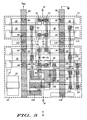
- BiCMOS macro 18 of FIG. 1 is shown in detail as an example to implement the NAND gate circuit shown in FIG. 2. It is understood that components similar to those shown in FIGs. 1 and 2 are designated by similar reference numerals.
- BiCMOS macro 18 includes one-half of CMOS cell 12 and BiCMOS cell 14. Thus, a full CMOS cell would be twice as large as shown in block 12 of FIG. 3 such that a typical CMOS cell would include two more additional P-type MOS transistors similar to transistors 28 and 30, and two more additional N-type MOS transistors similar to transistors 46 and 48.
- BiCMOS cell 14 is shown whereby two existing P-type MOS transistors of a typical CMOS cell have been replaced by two bipolar type transistors (transistors 34 and 35).
- Transistors 24, 26, 40, 42 and 44 all have their gate electrodes coupled to terminal 28 via metal contacts 60, 62, 64, 66, 67 and 68, respectively.
- transistors 28, 30, 46, 48 and 50 all have their gate electrodes coupled to terminal 32 via metal contacts 70, 72, 74, 76 and 78, respectively.
- Transistors 24, 26, 28 and 30 all have their source electrodes coupled to V DD metal bus 80 via metal contacts 82, 84, 86 and 88, respectively.
- transistors 46, 48 and 50 all have their source electrodes coupled to ground metal bus 90 via metal contacts 92, 94 and 96, respectively.
- the common drain electrodes of transistors 28 and 30 are coupled to the common drain electrodes of transistors 24 and 26 and to the base of bipolar transistor 34 via a metal layer having contacts 98, 100 and 102, respectively.
- the collector of bipolar transistor 34 is coupled to V DD metal bus 80 via metal contact 104.
- the emitter of bipolar transistor 34 is coupled to the drain electrodes of transistors 40, 42 and 44 via a metal layer having contacts 106, 108 and 110, respectively, whereby metal contact 108 is coupled to the common drain electrodes of transistors 40 and 42.
- resistor 38 is shown coupled between the base and emitter of bipolar transistor 34 via metal contacts 102 and 112, respectively.
- the emitter of bipolar transistor 34 is also coupled to terminal 36.
- the common drain electrodes of transistors 46 and 48 at metal contact 114 is coupled by metal layer 115 to the drain electrode of transistor 50 and to the source electrode of transistor 44 via metal contact 116.
- Metal layer 115 also couples the source electrodes of transistors 40 and 42 via metal contacts 118 and 120, respectively, to the source of transistor 44 (metal contact 116).
- metal contact 122 couples an N-well for P-type transistors 24, 26, 28 and 30 and for bipolar transistor 34 to operating potential V DD .
- metal contacts 124 and 126 couples a P-well (substrate) for N-type transistors 40, 42, 44, 46, 48 and 50 to ground reference. It is worth noting that bipolar transistor 35 is not being utilized by BiCMOS macro 18 for implementing the NAND gate circuit. However, another application may very well use bipolar transistor 35.
- CMOS complementary metal-oxide-semiconductor
- BiCMOS complementary metal-oxide-semiconductor
- various mixes of CMOS and BiCMOS cells can be utilized for performing a variety of macro functions such as an inverter circuit, a NOR gate circuit or a flip-flop circuit.
Landscapes
- Design And Manufacture Of Integrated Circuits (AREA)
- Metal-Oxide And Bipolar Metal-Oxide Semiconductor Integrated Circuits (AREA)
Applications Claiming Priority (2)
| Application Number | Priority Date | Filing Date | Title |
|---|---|---|---|
| US65012391A | 1991-02-04 | 1991-02-04 | |
| US650123 | 1991-02-04 |
Publications (1)
| Publication Number | Publication Date |
|---|---|
| EP0498567A1 true EP0498567A1 (de) | 1992-08-12 |
Family
ID=24607568
Family Applications (1)
| Application Number | Title | Priority Date | Filing Date |
|---|---|---|---|
| EP92300784A Withdrawn EP0498567A1 (de) | 1991-02-04 | 1992-01-30 | CMOS/BICMOS-Mischanordnung |
Country Status (2)
| Country | Link |
|---|---|
| EP (1) | EP0498567A1 (de) |
| JP (1) | JPH0575082A (de) |
Cited By (1)
| Publication number | Priority date | Publication date | Assignee | Title |
|---|---|---|---|---|
| EP0735684A3 (de) * | 1995-03-30 | 1998-11-11 | Nec Corporation | BiCMOS logische integrierte Schaltung |
Families Citing this family (1)
| Publication number | Priority date | Publication date | Assignee | Title |
|---|---|---|---|---|
| CN104111755B (zh) | 2014-07-24 | 2017-08-29 | 上海天马微电子有限公司 | 一种触控结构、触控面板及触控装置 |
Citations (2)
| Publication number | Priority date | Publication date | Assignee | Title |
|---|---|---|---|---|
| JPS63228641A (ja) * | 1987-03-18 | 1988-09-22 | Hitachi Ltd | 半導体集積回路装置 |
| EP0439301A1 (de) * | 1990-01-22 | 1991-07-31 | Hitachi, Ltd. | Integrierte Halbleiterschaltungsanordnung |
-
1992
- 1992-01-29 JP JP4036982A patent/JPH0575082A/ja active Pending
- 1992-01-30 EP EP92300784A patent/EP0498567A1/de not_active Withdrawn
Patent Citations (2)
| Publication number | Priority date | Publication date | Assignee | Title |
|---|---|---|---|---|
| JPS63228641A (ja) * | 1987-03-18 | 1988-09-22 | Hitachi Ltd | 半導体集積回路装置 |
| EP0439301A1 (de) * | 1990-01-22 | 1991-07-31 | Hitachi, Ltd. | Integrierte Halbleiterschaltungsanordnung |
Non-Patent Citations (2)
| Title |
|---|
| ELECTRONICS. vol. 61, no. 3, 4 February 1988, NEW YORK US pages 63 - 64; S. WEBER: 'LSI logic arrays boost both drive and density' * |
| PATENT ABSTRACTS OF JAPAN vol. 13, no. 26 (E-706)(3374) 20 January 1989 & JP-A-63 228 641 ( HITACHI LTD. ) 22 September 1988 * |
Cited By (2)
| Publication number | Priority date | Publication date | Assignee | Title |
|---|---|---|---|---|
| EP0735684A3 (de) * | 1995-03-30 | 1998-11-11 | Nec Corporation | BiCMOS logische integrierte Schaltung |
| US6037637A (en) * | 1995-03-30 | 2000-03-14 | Nec Corporation | BiCMOS logical integrated circuit |
Also Published As
| Publication number | Publication date |
|---|---|
| JPH0575082A (ja) | 1993-03-26 |
Similar Documents
| Publication | Publication Date | Title |
|---|---|---|
| EP0145004B1 (de) | Kombinierte Bipolartransistor-Feldeffekttransistor-Schaltung | |
| EP0591342B1 (de) | Basiszellen-architektur für maskenprogrammierbare gattermatrix | |
| KR890002966B1 (ko) | 마스터 슬라이스 집적회로 장치 | |
| EP0528956B1 (de) | Basiszelle für bicmos-gatterfeld | |
| EP0132822A2 (de) | Zusammengesetzte Schaltung aus bipolaren und Feldeffekt-Transistoren | |
| US6683335B2 (en) | Gate array layout for interconnect | |
| EP0013482A2 (de) | Komplementäre Metalloxyd-Halbleiteranordnung | |
| EP0177336B1 (de) | Integrierte Gate-Matrixstruktur | |
| US5635745A (en) | Analog multiplexer cell for mixed digital and analog signal inputs | |
| US5378941A (en) | Bipolar transistor MOS transistor hybrid semiconductor integrated circuit device | |
| JPH03190426A (ja) | 集積BiCMOS回路 | |
| JP2822781B2 (ja) | マスタスライス方式半導体集積回路装置 | |
| JP2632420B2 (ja) | 半導体集積回路 | |
| US4476479A (en) | Semiconductor device with operating voltage coupling region | |
| US5001487A (en) | Semiconductor integrated circuit device | |
| US5541439A (en) | Layout for a high voltage darlington pair | |
| JP3260509B2 (ja) | 半導体集積回路装置 | |
| US5066996A (en) | Channelless gate array with a shared bipolar transistor | |
| JP2661318B2 (ja) | 半導体装置 | |
| US6483131B1 (en) | High density and high speed cell array architecture | |
| KR950007345B1 (ko) | 바이폴라 트랜지스터·절연 게이트형 트랜지스터 혼재 반도체 장치 | |
| JPH0575082A (ja) | 混合CMOS/BiMOS装置 | |
| US5107147A (en) | Base cell for semi-custom circuit with merged technology | |
| JP2609746B2 (ja) | 半導体装置 | |
| JPH02172256A (ja) | 論理回路 |
Legal Events
| Date | Code | Title | Description |
|---|---|---|---|
| PUAI | Public reference made under article 153(3) epc to a published international application that has entered the european phase |
Free format text: ORIGINAL CODE: 0009012 |
|
| AK | Designated contracting states |
Kind code of ref document: A1 Designated state(s): DE FR GB |
|
| 18D | Application deemed to be withdrawn |
Effective date: 19930213 |