EP0498580A1 - Méthode dépôt d'un film métallique contenant de l'aluminium en utilisant un halide d'alkylaluminium - Google Patents
Méthode dépôt d'un film métallique contenant de l'aluminium en utilisant un halide d'alkylaluminium Download PDFInfo
- Publication number
- EP0498580A1 EP0498580A1 EP92300853A EP92300853A EP0498580A1 EP 0498580 A1 EP0498580 A1 EP 0498580A1 EP 92300853 A EP92300853 A EP 92300853A EP 92300853 A EP92300853 A EP 92300853A EP 0498580 A1 EP0498580 A1 EP 0498580A1
- Authority
- EP
- European Patent Office
- Prior art keywords
- electron donor
- substrate
- film
- deposition
- gas
- Prior art date
- Legal status (The legal status is an assumption and is not a legal conclusion. Google has not performed a legal analysis and makes no representation as to the accuracy of the status listed.)
- Ceased
Links
Images


Classifications
-
- H—ELECTRICITY
- H10—SEMICONDUCTOR DEVICES; ELECTRIC SOLID-STATE DEVICES NOT OTHERWISE PROVIDED FOR
- H10W—GENERIC PACKAGES, INTERCONNECTIONS, CONNECTORS OR OTHER CONSTRUCTIONAL DETAILS OF DEVICES COVERED BY CLASS H10
- H10W20/00—Interconnections in chips, wafers or substrates
- H10W20/01—Manufacture or treatment
- H10W20/031—Manufacture or treatment of conductive parts of the interconnections
- H10W20/056—Manufacture or treatment of conductive parts of the interconnections by filling conductive material into holes, grooves or trenches
- H10W20/057—Manufacture or treatment of conductive parts of the interconnections by filling conductive material into holes, grooves or trenches by selectively depositing, e.g. by using selective CVD or plating
-
- C—CHEMISTRY; METALLURGY
- C23—COATING METALLIC MATERIAL; COATING MATERIAL WITH METALLIC MATERIAL; CHEMICAL SURFACE TREATMENT; DIFFUSION TREATMENT OF METALLIC MATERIAL; COATING BY VACUUM EVAPORATION, BY SPUTTERING, BY ION IMPLANTATION OR BY CHEMICAL VAPOUR DEPOSITION, IN GENERAL; INHIBITING CORROSION OF METALLIC MATERIAL OR INCRUSTATION IN GENERAL
- C23C—COATING METALLIC MATERIAL; COATING MATERIAL WITH METALLIC MATERIAL; SURFACE TREATMENT OF METALLIC MATERIAL BY DIFFUSION INTO THE SURFACE, BY CHEMICAL CONVERSION OR SUBSTITUTION; COATING BY VACUUM EVAPORATION, BY SPUTTERING, BY ION IMPLANTATION OR BY CHEMICAL VAPOUR DEPOSITION, IN GENERAL
- C23C16/00—Chemical coating by decomposition of gaseous compounds, without leaving reaction products of surface material in the coating, i.e. chemical vapour deposition [CVD] processes
- C23C16/04—Coating on selected surface areas, e.g. using masks
-
- C—CHEMISTRY; METALLURGY
- C23—COATING METALLIC MATERIAL; COATING MATERIAL WITH METALLIC MATERIAL; CHEMICAL SURFACE TREATMENT; DIFFUSION TREATMENT OF METALLIC MATERIAL; COATING BY VACUUM EVAPORATION, BY SPUTTERING, BY ION IMPLANTATION OR BY CHEMICAL VAPOUR DEPOSITION, IN GENERAL; INHIBITING CORROSION OF METALLIC MATERIAL OR INCRUSTATION IN GENERAL
- C23C—COATING METALLIC MATERIAL; COATING MATERIAL WITH METALLIC MATERIAL; SURFACE TREATMENT OF METALLIC MATERIAL BY DIFFUSION INTO THE SURFACE, BY CHEMICAL CONVERSION OR SUBSTITUTION; COATING BY VACUUM EVAPORATION, BY SPUTTERING, BY ION IMPLANTATION OR BY CHEMICAL VAPOUR DEPOSITION, IN GENERAL
- C23C16/00—Chemical coating by decomposition of gaseous compounds, without leaving reaction products of surface material in the coating, i.e. chemical vapour deposition [CVD] processes
- C23C16/06—Chemical coating by decomposition of gaseous compounds, without leaving reaction products of surface material in the coating, i.e. chemical vapour deposition [CVD] processes characterised by the deposition of metallic material
- C23C16/18—Chemical coating by decomposition of gaseous compounds, without leaving reaction products of surface material in the coating, i.e. chemical vapour deposition [CVD] processes characterised by the deposition of metallic material from metallo-organic compounds
- C23C16/20—Deposition of aluminium only
-
- H—ELECTRICITY
- H10—SEMICONDUCTOR DEVICES; ELECTRIC SOLID-STATE DEVICES NOT OTHERWISE PROVIDED FOR
- H10P—GENERIC PROCESSES OR APPARATUS FOR THE MANUFACTURE OR TREATMENT OF DEVICES COVERED BY CLASS H10
- H10P14/00—Formation of materials, e.g. in the shape of layers or pillars
- H10P14/40—Formation of materials, e.g. in the shape of layers or pillars of conductive or resistive materials
- H10P14/42—Formation of materials, e.g. in the shape of layers or pillars of conductive or resistive materials using a gas or vapour
- H10P14/43—Chemical deposition, e.g. chemical vapour deposition [CVD]
- H10P14/432—Chemical deposition, e.g. chemical vapour deposition [CVD] using selective deposition
Definitions
- the present invention relates to a method of forming a metal film and, more particularly, to a method of forming an Al deposition film preferably applied to a wiring layer in a semiconductor integrated circuit device or the like.
- Aluminum (Al), Al-Si, and the like have been mainly used as materials for electrodes and wiring layers in conventional electronic devices and integrated circuits using semiconductors. Since Al is inexpensive, has a high electrical conductivity, and can form a dense oxide film on a surface, an internal structure can be chemically protected and stabilized by an Al deposition layer. In addition, Al has a high adhesion strength with Si, thus providing various advantages.
- an aspect ratio i.e., (length of via hole) ⁇ (diameter of via hole)
- an aspect ratio i.e., (length of via hole) ⁇ (diameter of via hole)
- the diameter of the via hole itself becomes 1 ⁇ m or less. Therefore, a technique for depositing Al in a via hole having a high aspect ratio is required.
- Al or the like must be deposited not only in the via hole but also on an insulating film. In addition, this deposition film must be excellent in quality.
- the present inventors have recently proposed a CVD method using a dimethylaluminum halide as a technique for forming an Al film.
- a method of forming a flat multi-layered wiring pattern including the step of forming an insulating film having a square contact hole having a side of 0.8 ⁇ m in a monocrystalline silicon substrate and selectively depositing monocrystalline aluminum in this contact hole by a CVD method using DMAH and hydrogen, the step of forming an electrode extraction layer consisting of a conductive material (e.g., W or titanium nitride) on the aluminum and the insulating layer, and the step of depositing aluminum on the entire surface.
- a conductive material e.g., W or titanium nitride
- disconnections and short circuits may be formed in wiring layers. This typically occurs in a wiring film having three or more layers.
- the present inventors have made various experiments and extensive studies to find a reason for reducing a product yield because the following causes interact each other.
- the first cause is formation of defects during initial aluminum deposition.
- the second cause is a problem of an interface between aluminum and an underlying material when aluminum is deposited in a contact hole defined by the underlying material.
- the third cause is a migration problem.
- a still another cause is a difference in yield between aluminum deposited in the contact hole and aluminum formed on the underlying layer, i.e., the insulating film during formation and a difference in film quality therebetween.
- It is still another object of the present invention to provide a method of forming a deposition film including the steps of: performing a chemical surface-treatment for causing an electron donor surface to terminate with hydrogen atoms in a substrate having the electron donor surface consisting of a non-monocrystalline material and a non-electron donor surface, and locating the substrate in a deposition film formation space; supplying a gas of an alkylaluminum halide and hydrogen gas to the deposition film formation space so that a partial pressure of the gas of the alkylaluminum halide falls within a range of 7 x 10 ⁇ 3 to 9 x 10 ⁇ 2 Torr; and selectively forming a metal film containing aluminum as a major constituent on the electron donor surface while the substrate is kept at a predetermined temperature which is not less than a decomposition temperature of the alkylaluminum halide and not more than 450°C.
- a method of forming a deposition film using an organic metal is summarized as follows.
- An organic metal deposition reaction and hence a thin-film deposition reaction greatly vary depending on conditions such as types of metal atoms, types of alkyl groups bonded to the metal atoms, a means for causing the decomposition reaction, and a gas atmosphere.
- a reaction form varies depending on the types of alkyl groups, types of metal atoms, and an excitation decomposition means.
- the decomposition reaction In order to deposit metal atoms decomposed from an organic metal on a desired substrate, the decomposition reaction must be strictly controlled.
- the decomposition reaction in order to deposit Al from triisobutylaluminum, i.e., in the following reaction, in a conventional low-pressure CVD using a thermal reaction, projections on the order of microns are formed on the surface, and a surface morphology is degraded. Hillocks are formed by annealing, and Si surface roughening occurs at an interface between Al and Si due to Si diffusion. In addition, migration durability is also degraded. It is therefore difficult to use this reaction in an industrial VLSI process.
- deposition film formation conditions in the CVD method using an organic metal are complicated due to a general nature wherein chemical properties of the organic metal are greatly changed in accordance with types and combinations of organic substituent groups bonded to metal atoms.
- a method of forming a deposition film must be a method of forming a high-quality film which can be applied in a relatively general range except for a limited application in which an apparatus is complicated due to the limited film formation conditions.
- the present inventors have prepared a large number of organic metals to find a condition which satisfies a standard applied to a large integrated circuit and made various experiments and extensive studies on different gas reaction states of reaction gases, different carrier gases, and different substrate temperatures.
- the present inventors have found that an alkylaluminum halide is used as a source gas to satisfy a parameter for providing highly general film formation conditions.
- film formation conditions preferably applied to large integrated circuits are given as follows.
- An alkylaluminum halide gas is used as a source gas
- H2 gas is used as a reaction gas
- a substrate has an electron donor surface (A) and a non-electron donor surface (B).
- the temperature of the electron donor surface is the decomposition temperature or more of the alkylaluminum halide and is 450°C or less.
- Dimethylalkylaluminum halide (DMAH) as an alkylaluminum halide according to the present invention is a known material as an alkyl metal.
- a relationship between reaction forms and Al thin films to be deposited cannot be expected unless deposition films are formed under all possible conditions.
- DMAH Dimethylalkylaluminum halide
- a surface morphology is degraded, and a resistivity falls within the range of several ⁇ cm to 10 ⁇ cm, whose smallest value is larger than a bulk value (2.7 ⁇ cm).
- film quality is poor.
- a CVD method is used to selectively deposit a high-quality Al or Al-Si film as a conductive deposition film on a substrate.
- Dimethylaluminum halide (DMAH) represented by the following formula: or monomethylalkylaluminum halide (MMAH2) represented by the following formula: is used as a source gas having at least one atom constituting one of the components of a deposition film, and H2 is used as a reaction gas. These gases are mixed to epitaxially grow an Al film on a substrate.
- DMAH dimethylaluminum halide
- MMAH2 monomethylaluminum halide
- Si as a source gas
- H2 is used as a reaction gas.
- a mixture of these gases is used to epitaxially grow an Al-Si film on a substrate.
- the partial pressure of alkylaluminum halide as the source gas particularly falls within the range of 7 x 10 ⁇ 3 to 9 x 10 ⁇ 2 Torr.
- Al is deposited under this pressure condition, an Al film excellent in stress migration durability can be obtained.
- a substrate applied to the present invention has a first substrate surface material for forming a surface on which Al is to be deposed and a second substrate surface material for forming a surface on which Al is not deposited.
- An electron donor material is used as the first substrate surface material.
- the electron donor will be described in detail below.
- the electron donor material is a material in which free electrons are present in a substrate or free electrons are intentionally produced.
- the electron donor material is defined as a material having a surface on which a chemical reaction is accelerated by electron exchange with source gas molecules attached to the substrate surface.
- a material having a thin oxide film on its surface is also defined as the electron donor material because a chemical reaction occurs due to electron exchange between the substrate and the material molecules attached to the substrate surface.
- the electron donor materials are p- and n-type semiconductors (e.g., monocrystalline silicon, polysilicon, and amorphous silicon), a two-, three-, or four-component Group III-V compound semiconductor as a combination of Ga, In, or Al as a Group III element and P, As, or N as a Group V element, and a metal, an alloy, and a silicide, which latter three are exemplified by tungsten, molybdenum, tantalum, tungsten silicide, titanium silicide, aluminum, aluminum/silicon, titanium/aluminum, titanium nitride, copper, aluminum/silicon/copper, aluminum/palladium, titanium, molybdenum silicide, and tantalum silicide.
- tungsten, molybdenum, tantalum tungsten silicide, titanium silicide, aluminum, aluminum/silicon, titanium/aluminum, titanium nitride, copper, aluminum/silicon/copper, aluminum/pal
- a material for forming a surface on which Al or Al-Si is not selectively deposited i.e., a non-electron donor material
- silicon oxide formed by thermal oxidation, CVD, sputtering, or the like glass (e.g., BSG, PSG, or BPSG), an oxide film, a thermal nitride film, and a silicon nitride film formed by plasma CVD, low-pressure CVD, ECR-CVD, or the like.
- Al is deposited on such a substrate by a simple thermal reaction in a reaction system between a source gas and H2.
- a thermal reaction in a reaction system between, e.g., DMAH and H2 is performed at a substrate temperature of 160°C to 450°C as follows:
- DMAH methyl methacrylate
- Al-Si can be deposited on only a surface having an electron donor material.
- DMAH and H2 are used to deposit pure Al.
- DMAH, Si2H6, and H2 are used to deposit Al-Si.
- Figs. 1(a) to 1(e) are views showing the steps in selective growth using a combination of DMAH and H2 or a combination of DMAH, Si2H6, and H2.
- Fig. 1(a) is a view illustrating a substrate section before an Al or Al-Si deposition film is formed.
- a substrate 90 consists of an electron donor material and is exemplified as an Si wafer.
- a thin film 91 consists of a non-electron donor material and is exemplified as a thermal oxidation SiO2 film or a BSG film.
- a chemical treatment (to be described in detail later) of the substrate is performed as a pre-treatment of deposition, so that terminal bonds of surface atoms are terminated as a hydrogen atom group.
- the Al-Si film is grown to the uppermost level of the thin film 91, as shown in Fig. 1(d) through a state in Fig. 1(c).
- the Al-Si film can be grown to a thickness of 5,000 ⁇ almost without extending in the lateral direction, as shown in Fig. 1(e).
- This growth is a characteristic feature of a deposition film formed using the combination of DMAH and H2 or the combination of DMAH, H2, and Si2H6. It can be understood that a high-quality film can be formed with good selectivity.
- the resultant film does not contain impurities such as carbon and oxygen in accordance with analysis results using an Auger electron spectroscopy or photoelectron spectroscopy.
- a 4,000- ⁇ thick deposition film thus obtained has a resistivity of 2.7 to 3.0 ⁇ cm, which is almost equal to that of Al bulk at room temperature. This film is continuous and flat. Even if a deposition film has a thickness of 1 ⁇ m, its resistivity falls within the range of 2.7 to 3.0 ⁇ cm at room temperature. Therefore, even a thick deposition film can be a sufficiently dense film.
- the reflectance of a deposition film in a wavelength range of visible light is about 80%. A thin film having excellent surface flatness and excellent stress migration can be deposited.
- a technique for selectively embedding a via hole with high-quality Al or Al-Si is indispensable.
- Al or Al-Si is selectively deposited, as shown in Fig. 1(d)
- a non-electron donor material e.g., a thermal oxidation SiO2 film or a CVD-BSG film
- a highly reliable multi-layered wiring process free from disconnections at stepped portions can be realized.
- the alkylaluminum halide and H2 in the selective growth on the electron donor surface heated to the decomposition temperature or more of the alkylaluminum halide and 450°C or less, excellent selectivity of the Al film can be obtained. For this reason, a technique for forming an Al film on the thin film 91 must be implemented. In consideration of this, the non-electron donor surface is modified, and an Al film which cannot be deposited on the non-electron donor surface due to its selectivity can be formed on the modified non-electron donor surface.
- This surface modification can be performed by the step of supplying electrons and hydrogen to the non-electron donor substrate surface.
- the following point in combination with the sputtering method can be improved. That is, after the CVD process, a wafer is exposed to the atmospheric air when the wafer is transferred to another sputtering apparatus. A high-resistance film containing oxygen is formed at an interface between the selectively grown Al film and a non-selectively grown Al film to increase a contact resistance to fail to realize a low-resistance wiring pattern. This drawback can be eliminated by the above method.
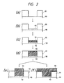
- Figs. 2(a) to 2(e) are views showing the steps in selective formation on an electron donor surface consisting of a non-monocrystalline material by using a combination of DMAH and H2 or a combination of DMAH, Si2H6, and H2.
- An underlying material on which Al for forming a wiring electrode is formed is generally constituted by a non-monocrystalline material. More specifically, examples of the underlying material are polysilicon for forming a gate electrode or a wiring layer, a metal silicide material such as W silicide or Mo silicide for forming a polycide structure, and a W, WSi2, Mo, or MoSi2 barrier material for preventing diffusion of Si and Al.
- the polysilicon, the metal silicide material, and the barrier metal material can be patterned into desired shapes by photolithographic techniques.
- An insulating film is deposited on the entire surface of the resultant structure, a contact hole is formed in this insulating film, and an electrode material is embedded in the contact hole, thereby forming a wiring layer.
- the cleaning time using HF/H2O is 60 seconds, and final cleaning with water is performed for 6 minutes.
- TDS method terminal hydrogen atoms are observed on the surfaces of polysilicon, a silicide material, and a barrier material in main cleaning.
- Selective deposition of Al by using DMAH can be performed on the basis of the mechanism described above.
- Fig. 2(a) is a view illustrating a substrate section before formation of an Al or Al-Si deposition film.
- a substrate 90 consists of an electron donor material and is exemplified by an Si wafer.
- a thin film 91 consists of a non-electron donor material and is exemplified by a thermal oxidation SiO2 film or a BSG film.
- polycrystalline W is selectively deposited in a hole by using WF6 gas.
- a chemical treatment of the substrate is performed as a pre-treatment, and the surface of the W film 92 is terminated with a hydrogen atom group.
- the Al-Si film is grown to the uppermost level of the thin film 91, as shown in Fig. 2(d) through a state in Fig. 2(c).
- the Al-Si film can be grown to a thickness of 5,000 ⁇ almost without extending in the lateral direction, as shown in Fig. 2(e).
- This growth is a characteristic feature of a deposition film formed using the combination of DMAH and H2 or the combination of DMAH, H2, and Si2H6. It can be understood that a high-quality film can be formed with good selectivity.
- the resultant film does not contain impurities such as carbon and oxygen in accordance with analysis results using an Auger electron spectroscopy or photoelectron spectroscopy.
- a 4,000- ⁇ thick deposition film thus obtained has a resistivity of 2.7 to 3.0 ⁇ cm, which is almost equal to that of Al bulk at room temperature. This film is continuous and flat. Even if a deposition film has a thickness of 1 ⁇ m, its resistivity falls within the range of 2.7 to 3.0 ⁇ cm at room temperature. Therefore, even a thick deposition film can be a sufficiently dense film.
- the reflectance of a deposition film in a wavelength range of visible light is about 80%. A thin film having excellent surface flatness and excellent stress migration can be deposited.
- a technique for selectively embedding a via hole with high-quality Al or Al-Si is indispensable.
- Al or Al-Si is selectively deposited, as shown in Fig. 2(d)
- a non-electron donor material e.g., a thermal oxidation SiO2 film or a CVD-BSG film
- a highly reliable multi-layered wiring process free from disconnections at stepped portions can be realized.
- the alkylaluminum halide and H2 in the selective growth on the electron donor surface heated to the decomposition temperature or more of the alkylaluminum halide and 450°C or less, excellent selectivity of the Al film can be obtained. For this reason, a technique for forming an Al film on the thin film 91 must be implemented. In consideration of this, the non-electron donor surface is modified, and an Al film which cannot be deposited on the non-electron donor surface due to its selectivity can be formed on the modified non-electron donor surface.
- This surface modification can be performed by the step of supplying electrons and hydrogen to the non-electron donor substrate surface.
- the following point in combination with the sputtering method can be improved. That is, after the CVD process, a wafer is exposed to the atmospheric air when the wafer is transferred to another sputtering apparatus. A high-resistance film containing oxygen is formed at an interface between the selectively grown Al film and a non-selectively grown Al film to increase a contact resistance to fail to realize a low-resistance wiring pattern. This drawback can be eliminated by the above method.
- Al or Al-Si shown in Fig. 2(f) can be deposited by one CVD apparatus.
- the function of the present invention is as follows. Deposition is performed to fill the via hole using the combination of DMAH and H2 or the combination of DMAH, Si2H6, and H2, as shown in Figs. 2(a) to 2(e).
- the surface of the non-electron donor surface is modified into a substantially electron donor material surface.
- Al or Al-Si is uniformly deposited on the Al or Al-Si surface serving as the electron donor material and the modified non-electron donor material as the electron donor material.
- the surface modification is to modify even a non-electron donor surface such that free electrons are present and contribute to a surface reaction. For example, there is a method of supplying free electrons to the surface by a plasma process, ion radiation, or electron beam radiation. Another method is also available in which light having an energy higher than that of a forbidden band width of SiO2 is radiated on SiO2 to produce free electrons on the non-electron donor surface.
- H2 molecules are dissociated into H atoms, as is well known, to react with the DMAH present on the non-electron donor surface and continuous flowing thereon, thereby depositing an Al film.
- H atoms and electrons may be directly supplied from the H2 plasma to the surface of the non-electron donor surface and are reacted with the DMAH to form an Al film. According to an assumption to be described later, DMAH must contain asymmetric molecules.
- the DMAH molecules have a reaction group CH3 for causing a surface reaction on the modified surface and a heredity radical H (for forming a surface equivalent to a modified surface) indispensable to continuation of the reaction, deposition by the reaction on the substrate surface and continuation of the reaction can be performed.
- An electron density in the plasma near the substrate surface subjected to surface modification falls within the range of 1 x 108 cm ⁇ 3 to 8 x 1010 cm ⁇ 3, and more preferably 5 x 108 cm ⁇ 3 to 2 x 109 cm ⁇ 3 near the substrate surface.
- a plasma power density preferably falls within the range of 0.04 to 0.4 W/cm3.
- An area near the substrate surface includes a 1-cm deep area from the substrate surface. More specifically, the electron density at the center of the plasma is 1 x 1010 cm ⁇ 3 and that near the substrate surface is 1 x 108 cm ⁇ 3.
- the electron density is measured by a known TDS or HEELS method.
- the electron density of the present invention is determined by such a method.
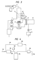
- Fig. 3 is a view showing a deposition film formation apparatus which can be applied to the present invention.
- An Al-Si film is to be formed on a substrate 1.
- the substrate 1 is placed on a substrate holder 3 arranged inside a reaction tube or chamber 2 for forming a substantially closed deposition film formation space.
- a material for forming the reaction tube 2 is preferably quartz, but may be a metal. If a metal is used to form the reaction tube 2, the reaction tube 2 is preferably cooled.
- the substrate holder 3 is made of a metal and incorporates a heater 4 to heat the substrate placed thereon. The temperature of the heater 4 is controlled to control the substrate temperature.
- a gas supply system 56 is arranged as follows.
- a supply system using low-pressure bubbling is preferably employed to change a partial pressure of DMAH.
- a gas supply unit using the low-pressure bubbling is shown in Fig. 4.
- Hydrogen gas supplied from a supply gas line 110 is supplied to a bubbler 104 through a supply gas main line 108 after the flow rate of the hydrogen gas is controlled by a flow control unit 101.
- the bubbler 104 contains DMAH or the like.
- the predetermined partial DMAH pressure which can achieve the object of the present invention can be obtained on the basis of the above equation.
- the total pressure P TOT of the reaction chamber is set to be 1.5 Torr
- the pressure P B inside the bubbler 104 is controlled to be 100 Torr by the pressure control unit 105, so that the partial pressure P DMAH of the DMAH supplied to the reaction chamber is set to be 3 x 10 ⁇ 2 Torr by the above equation.
- the internal pressure P B of the bubbler can be increased about 10 times 1 atm.
- Similar control operations are performed to change the internal pressure P B of the bubbler in the range of 760 Torr to 14 Torr, so that the partial pressure of the DMAH can be changed in the range of 4.0 x 10 ⁇ 3 to 2.1 x 10 ⁇ 1 Torr.
- the partial pressure of the DMAH can be reduced as follows. As shown in Fig. 4, the internal pressure of the bubbler is set close to 1 atm., and hydrogen gas from the supply gas line 110 is partially supplied to a supply gas bypass line 109. This hydrogen gas is supplied to the reaction tube 106 together with hydrogen gas supplied from a supply gas main line 108 containing DMAH, thereby substantially reducing the partial pressure of the DMAH.
- the partial pressure of the DMAH can be controlled by a hydrogen flow rate ratio of the hydrogen flowing through the main line 108 to that flowing through the bypass line 109.
- An evacuation system has the following arrangement.
- a gate valve 7 is opened to perform large-capacity evaluation as in evaluation of the interior of the reaction tube 2 prior to formation of the deposition film.
- a slow leak valve 8 is used to perform small-capacity evaluation as in adjustment of the internal pressure of the reaction tube 2 during formation of the deposition film.
- An evacuation unit 9 is constituted by an evacuation pump such as a turbo molecular pump.
- a convey system of the substrate 1 is arranged as follows.
- a substrate convey chamber 10 can store a substrate before and after formation of the deposition film.
- the substrate convey chamber 10 can be evacuated by opening a valve 11.
- An evacuation unit 12 is used to evacuate the convey chamber 10 and is constituted by an evacuation pump such as a turbo molecular pump.
- a valve 13 is open during only transfer of the substrate 1 between the reaction chamber and the convey space.
- An electrode 16 serving as a plasma generating means is arranged around the reaction chamber 2.
- An AC power source 14 is connected to the electrode 16 to generate a plasma.
- the liquid DMAH held at room temperature is bubbled with H2 or Ar (or any other inert gas) as a carrier gas to produce gaseous DMAH.
- the DMAH gas is then supplied to a mixer 14.
- H2 as the reaction gas is supplied to the mixer 14 through another supply path. The flow rates of these gases are controlled so that the respective partial pressures are set to be predetermined pressures.
- MMAH2 may be used as the first source gas.
- DMAH having a vapor pressure set to be 1 Torr at room temperature is most preferable.
- a mixture of DMAH and MMAH2 may be used.
- Si-containing gas as the second source gas for forming an Al-Si film examples include Si2H6, SiH4, Si3H6, Si(CH3)4, SiCl4, SiH2Cl, and SiH3Cl. Among them all, Si2H6 is most preferable because it tends to be decomposed at a low temperature of 200 to 300°C.
- Si2H6 gas diluted with H2 or Ar is obtained by supplying DMAH to the mixer through another flow path and is supplied to the reaction tube 2.
- an Si-containing gas or a Ti-containing gas such as TiCl4 is supplied to the mixer through a pipe different from those for the DMAH and the Si-containing gas, and the resultant gas is supplied from the mixer to the reaction tube 2.
- the Al-Si film is grown to the uppermost level of the thin film 91, as shown in Fig. 1(d) through a state in Fig. 1(c).
- the selectively deposited pure Al film is of monocrystalline.
- the "surface modification process" which causes a surface reaction on the non-electron donor surface is performed while DMAH and Si2H6 are kept supplied. DMAH and Si2H6 are then kept supplied to deposit Al or Al-Si in a shape shown in Fig. 1(f).
- the substrate is preferably kept at the predetermined temperature which is the decomposition temperature or more of the Al-containing source gas and 450°C or less. More specifically, the substrate temperature preferably falls within the range of 200 to 450°C.
- the deposition rate is as very large as 1,000 ⁇ /min to 3,000 ⁇ /min when the partial pressure of the DMAH is the internal pressure of the reaction vessel of 7 x 10 ⁇ 3 to 9 x 10 ⁇ 2 Torr. A high deposition rate in a VLSI Al-Si deposition technique can be obtained.
- the substrate temperature more preferably falls within the range of 270°C to 350°C, and orientation of the Al-Si film deposited under this condition is uniform. Even if annealing at 450°C for 1 hour is repeated several tens of times, hillocks and spikes are not formed on Al-Si films on a monocrystalline silicon substrate or a polysilicon substrate, thereby obtaining a high-quality Al-Si film. This Al-Si film is excellent in electromigration durability.
- the surface modification process is performed as follows.
- An H2 plasma is generated by RF power in an H2 atmosphere in the reaction tube.
- H atoms and electrons are supplied from the plasma to the non-electron donor surface to modify the non-electron donor surface to a substantially electron donor surface, thereby allowing deposition shown in Fig. 1(f).
- Ground electrodes 16′ and 16 ⁇ are arranged as plasma generation electrodes in addition to the electrode 16.
- an RF power having a frequency of about 13.56 MHz is applied to the electrode 16 to generate a plasma.
- the electrode 16 Since the electrode 16 is interposed between the ground electrodes 16′ and 16 ⁇ , lines of electric force from the excitation electrode 16 are terminated at the ground electrodes 16 ⁇ and 16′, thereby minimizing damage to the substrate 1 by the plasma.
- Al or Al-Si is selectively deposited on the electron donor surface of the substrate having the electron donor surface and the non-electron donor surface, and a plasma is generated while the combination of DMAH and H2 or the combination of DMAH, H2, and Si2H6 are kept supplied.
- the electrons and hydrogen atoms are supplied from the plasma to the non-electron donor surface to perform surface modification. After the surface modification is completed, the plasma is stopped, and deposition is continued.
- the DMAH is excited and decomposed to produce a large nucleus having Al as a major constituent in the surface modification process, thereby greatly degrading the surface morphology.
- the plasma power and the electron density are excessively low, supply of the electrons and hydrogen atoms becomes insufficient, thereby reducing the surface modification effect.
- the pressure of the reaction tube during surface modification falls within the range of 0.1 to 5 Torr, the plasma generation power falls within the range of 0.04 to 0.4 W/cm ⁇ 3 in the apparatus shown in Fig. 4, the surface modification time is 10 sec or more, and the electron density of the plasma near the substrate surface falls with the range of 5 x 108 cm ⁇ 3 to 2 x 109 cm ⁇ 3.
- Al is non-selectively deposited on the electron donor surface and the modified non-electron donor surface.
- no carbon is detected on the Al or Al-Si selectively deposited on the electron donor surface and the Al or Al-Si non-selectively deposited on the electron donor surface and the modified non-electron donor surface.
- the film quality of the Al or Al-Si deposited while generating the plasma is almost equal to that of the film deposited without any plasma.
- the density of the plasma power applied during the surface modification is smaller than a plasma power used in conventional CVD or conventional reactive ion etching. For this reason, almost no material is deposited on the inner wall surface of the reaction tube.
- the 13.56-MHz RF power source is used to generate the plasma.
- a DC, commercial frequency, or microwave (e.g., 2.45 GHz) power may be used to perform an electric discharge.
- Selective growth is determined such that a reaction for forming a desired film is formed on a substrate surface.
- Whether selective growth occurs or not can be described by a difference in adsorption point on the substrate surface.
- selectivity is exhibited by the difference in adsorption point, e.g., when the growth time is prolonged or the deposition temperature is increased, deposition selectivity is impaired.
- a deposition film In order to apply selective growth to a VLSI process, a deposition film must have high quality, and good selectivity must be obtained. That is, nuclei and the like should not be formed on a surface free from film deposition.
- Al deposition associated with the present invention Al is deposited on the electron donor surface, but no Al nucleus is formed on the non-electron donor surface, thereby obtaining excellent selectivity.
- An Al deposition reaction can be represented by formula (1) as a whole. It is difficult to expect from only equation (1) whether selective growth occurs. Excellent selectivity of the present invention can be readily understood when the reaction represented by formula (1) is microscopically observed.
- monocrystalline Al can be deposited on a monocrystalline Si substrate in an embodiment to be described below.
- the reaction represented by formula (1) will be exemplified by Al deposition on a monocrystalline Si substrate.
- Cleaning using an ammonia-based solution and a treatment using sulfuric acid-based chemicals are generally performed, and the resultant structure is dipped in a diluted hydrofluoric acid solution.
- the structure is removed from the diluted hydrofluoric acid solution and is cleaned with water.
- the Si surface is terminated with H atoms, as indicated by formula (A) in Fig. 5.
- Si and O bonds on the SiO2 surface are closed, and H atoms are not terminated.
- Si-H forms an electric double layer due to electron movement since electronegativity of Si is less than that of H as follows: Si + ⁇ -H - ⁇
- H2 is dissociated on the Si surface into H atoms, so that the H atoms are terminated to uncombined Si on the Si surface.
- DMAH has a dimer structure at room temperature, but is heated and converted into a monomer on the substrate, so that DMAH is adsorbed in the substrate surface. More specifically, the DMAH is adsorbed such that the CH3 group is located on the substrate surface side, as indicated by formula (A) of Fig. 5.
- the Al-CH3 bond is said to be weakened in the presence of free electrons on a surface where the free electrons are present. It is known in the chemical field that the CH3 group is reacted with the H atoms at the zero activation energy level to produce CH4 by reaction formula (B) of Fig. 5 (to be referred to as a methanization reaction hereinafter).
- the terminated H atoms on the Si surface are given as follows: H - ⁇ and tend to be reacted with the CH3 having a small electron affinity.
- the methanization reaction tends to occur by a catalyst function of the free electrons present on the surface.
- the CH3 group is reacted with H2 molecules to produce CH4.
- the reaction speeds are different from each other by ten times or more.
- the CH3 group is reacted with the H atoms to cause the methanization reaction.
- Al is deposited on Si as the electron donor substrate through the reactions represented by formulas (A) and (B) in Fig. 5. At this time, it is important that the source gas DMAH has the CH3 group which tends to be selectively reacted with the terminated atoms on the substrate surface.
- Al is deposited through the reactions represented by formulas (A) and (B) of Fig.
- the Al surface is set in a state wherein the H atoms are terminated, as indicated by formula (C) in Fig. 5. This state is the same as the initial state represented by formula (A) in Fig. 5. Since free electrons are present in Al, the H2 molecules are dissociated into H atoms, and the Al surface can be terminated with H.
- Al deposition continuously occurs by DMAH adsorption and the methanization reaction.
- the H atoms for terminating the Al surface upon deposition of Al are H atoms in the DMAH.
- the H atoms in the DMAH can be called a heredity radical capable of maintaining the terminated state.
- the CH3 in the DMAH can be called a selectivity reacting radical for selectively reacting with the atoms terminated on the surface.
- the Al deposition reaction is caused by a selective reaction between the H atoms terminated on the surface and the CH3 group in the DMAH.
- Supply of the terminating H atoms is achieved by dissociation of H2 molecules on the electron donor substrate surface on which free electrons are present.
- supply of terminating H atoms is achieved by free electrons on the electron donor substrate surface which cause the methanization reaction.
- a non-electron donor substrate surface such as an SiO2 surface is not terminated with H atoms. Free electrons are not present on the non-electron donor substrate surface. Even if a large number of H2 molecules are supplied to this surface, neither dissociation occurs nor a terminated state is obtained. In this manner, since the free electrons are present, the Al-CH3 bond is not weakened, and the reaction CH3 + H ⁇ CH4 does not occur. Therefore, since the terminated H atoms for causing Al deposition and the free electrons for causing the above reaction are not present, no Al deposition occurs on the non-electron donor substrate.
- the above reaction is apparently caused by the terminated state of the surface and the free electrons for causing the reaction.
- the structure of the DMAH molecule is also a characteristic feature in which different groups such as CH3 group and the H atoms are bonded around Al atoms.
- DMAH molecules i.e., the growing atoms constituting the deposition film
- different materials i.e., the CH3 group and the H atoms, are bonded to the Al molecules are called asymmetrical molecules.
- Al growth on monocrystalline silicon is taken into consideration again. As described above, when the Si surface is chemically treated, the surface is terminated with H atoms. It should be noted that the H atoms terminated on the monocrystalline Si are two-dimensionally, regularly aligned. Therefore, Al deposited on monocrystalline Si becomes of monocrystalline.
- a metal such as Al constituting an electron donor substrate or the like on which free electrons are present the surface is terminated with H atoms by the terminated H atoms dissociated from H2 molecules in the presence of free electrons or by dissociation/adsorption of the H atoms as in W having d electrons. Therefore, Al is deposited on only the electron donor substrate by the reactions represented by formulas (A), (b), and (C) in Fig. 5.
- a film obtained by an Al or Al-Si film formation method according to the present invention is dense and has a very small amount of impurities such as carbon.
- the film has a resistivity almost equal to the bulk and has a high flatness.
- the film has the following typical effects:
- a deposition film can be selectively formed in a recess in a substrate having surface roughness on a micron or submicron order and having an electron donor material and a non-electron donor material.
- a uniform Al film can be formed on the entire substrate within the same film formation apparatus.
- a decrease in thickness of a metal thin film on the rough surface degrades the reliability of the device.
- a decrease in film thickness on the rough surface is small, and a highly reliable Al or Al-Si film can be formed.
- a wall portion of an opening formed in an insulating film is inclined by a technique such as a reflow technique using, e.g., high-temperature annealing.
- the method of the present invention is ideal as a method of depositing a metal wiring layer for a micropatterned VLSI.
- the substrate surface is terminated with H and F atoms.
- Final cleaning with water can eliminate most of the F atoms.
- a stable state can be obtained in which H atoms are terminated on the substrate surface.
- Deposition was performed in the following examples using the pre-treated substrates.
- the surface of a monocrystalline Si substrate is thermally oxidized and is patterned to form a hole.
- a thin polycrystalline W film is formed in the hole by a selective CVD method using WF6. Thereafter, the chemical pre-treatment described above is performed.
- the reaction tube 2 is evacuated to about 1 x 10 ⁇ 8 Torr by the evaluation unit 9. Note that Al is grown even if the degree of vacuum in the reaction tube 2 is less than 1 x 10 ⁇ 8 Torr.
- the Si wafer having the W film described is cleaned with the chemical pre-treatment.
- the convey chamber 10 is set at the atmospheric pressure to load the Si wafer in the convey chamber.
- the convey chamber is evacuated to about 1 x 10 ⁇ 6 Torr, the gate valve 13 is opened, and the wafer is held in the wafer holder 3.
- the gate valve 13 is closed, and the reaction chamber 2 is evacuated to about 1 x 10 ⁇ 8 Torr.
- DMAH is supplied from the first gas line.
- a carrier gas for the DMAH line is H2.
- the second gas line is used for H2.
- H2 is supplied from the second line and the opening degree of the slow leak valve 8 is controlled to set the internal pressure of the reaction tube 2 to a predetermined value.
- a typical pressure in this example is about 1.5 Torr.
- the heater 4 is energized to heat the wafer.
- DMAH is supplied from the DMAH line to the reaction tube.
- the total pressure is about 1.5 Torr, and the partial pressure of DMAH is set to be about 1.5 x 10 ⁇ 4 Torr.
- this DMAH is supplied to the reaction tube 2, Al is deposited. This Al film is defined as the first Al film.
- a voltage is applied from an RF (13.56 MHz) power source to the excitation electrode 16 without interrupting DMAH supply, thereby generating an H2 plasma.
- Ring-like electrodes are arranged to interpose the ring-like electrode applied with the RF power and are set at the ground potential, so that the plasma can be properly shaped.
- the decomposition reaction is performed by a plasma by an RF power of 20 W, an electron density of 1 x 109 cm ⁇ 3 near the substrate surface, and an electron temperature of 6.5 eV near the substrate surface. That is, the hydrogen atoms and the electrons are supplied from the plasma to the substrate, thereby performing a surface modification process.
- Al is not deposited on SiO2, but Al is deposited on only the Si-exposed portion to a thickness equal to that of SiO2.
- Al is deposited on both the first Al film and SiO2 at the same deposition rate.
- the heater 4 is stopped, and the wafer is cooled.
- Supply of the H2 gas is stopped, and the reaction vessel is evacuated.
- the wafer is transferred to the convey chamber. Only the convey chamber is set at the atmospheric pressure, and the wafer is unloaded.
- Si substrate n-type; 1 to 2 ⁇ cm
- a hydrogen combustion system H2: 41/M; O2: 21/m
- the film thickness fell within the range of 7,000 ⁇ ⁇ 500 ⁇ , and the refractive index was 1.46.
- a photoresist was applied to the entire surface of the Si substrate, and a desired pattern was printed by a stepper. This pattern had various holes having sizes ranging from 0.25 ⁇ m x 0.25 ⁇ m to 100 ⁇ m x 100 ⁇ m.
- the photoresist was developed to obtain a photoresist pattern, and underlying SiO2 was etched using the photoresist pattern as a mask by reactive ion etching (RIE), thereby partially exposing the Si substrate.
- 130 samples having holes which had various sizes ranging from 0.25 ⁇ m x 0.25 ⁇ m to 100 ⁇ m x 100 ⁇ m and were formed in SiO2 were prepared.
- W barrier metal layers each having a thickness of about 500 ⁇ were formed on the respective samples by a CVD method using WF6. Following the same procedures as described above, Al was deposited on these 130 samples at 13 different substrate temperatures in units
- the conditions in the first Al film deposition process, the surface modification process, and the second Al film deposition process are as follows.
- Al was selectively deposited on only the Si-exposed portions to have the same thickness as that of SiO2 in the first Al deposition process.
- Al was deposited on both the Al film deposited in the first Al film deposition process and the SiO2 surface at the same deposition rate.
- the Al film selectively formed on Si and the Al film deposited on SiO2 upon surface modification had identical film quality in resistivity, reflectance, and hillock generation density upon annealing.
- Square contact holes each having a side of 1 ⁇ m were formed in each monocrystalline wafer such that the surface of the wafer had an aspect ratio of 1 or more, thereby obtaining 12 wafers.
- the number of contact holes in each wafer was 500,000.
- the number of wiring patterns free from defects is defined as M.
- Example 3 Samples (two samples for each sample No.) formed in Example 3 were prepared. These samples were heated in an N2 atmosphere at 600°C, and most of the adsorbed hydrogen atoms were eliminated.
- Al or Al-Si can be deposited in micropatterned via holes having a high aspect ratio and Al or Al-Si wiring patterns can be formed therein. Therefore, the present invention is effective as a micropatterning technique for LSIs, and the yield of LSIs can be further increased.
- the reaction tube 2 is evacuated to about 1 x 10 ⁇ 8 Torr by the evaluation unit 9. Note that Al is grown even if the degree of vacuum in the reaction tube 2 is less than 1 x 10 ⁇ 8 Torr.
- the convey chamber 10 is set at the atmospheric pressure to load the Si wafer in the convey chamber.
- the convey chamber is evacuated to about 1 x 10 ⁇ 6 Torr, the gate valve 13 is opened, and the wafer is held in the wafer holder 3.
- the gate valve 13 is closed, and the reaction chamber 2 is evacuated to about 1 x 10 ⁇ 8 Torr.
- DMAH is supplied from the first gas line.
- a carrier gas for the DMAH line is H2.
- the second gas line is used for H2.
- H2 is supplied from the second line and the opening degree of the slow leak valve 8 is controlled to set the internal pressure of the reaction tube 2 to a predetermined value.
- a typical pressure in this example is about 1.5 Torr.
- the heater 4 is energized to heat the wafer.
- DMAH is supplied from the DMAH line to the reaction tube.
- the total pressure is about 1.5 Torr, and the partial pressure of DMAH is set to be about 2 x 10 ⁇ 2 Torr.
- Al is deposited. This Al film is defined as the first Al film.
- a voltage is applied from an RF (13.56 MHz) power source to the excitation electrode 16 without interrupting DMAH supply, thereby generating an H2 plasma.
- Ring-like electrodes are arranged to interpose the ring-like electrode applied with the RF power and are set at the ground potential, so that the plasma can be properly shaped.
- the decomposition reaction is performed by a plasma by an RF power of 20 W, an electron density of 1 x 109 cm ⁇ 3 near the substrate surface, and an electron temperature of 6.5 eV near the substrate surface. That is, the hydrogen atoms and the electrons are supplied from the plasma to the substrate, thereby performing a surface modification process.
- Al is not deposited on SiO2, but Al is deposited on only the Si-exposed portion to a thickness equal to that of SiO2.
- Al is deposited on both the first Al film and SiO2 at the same deposition rate.
- the heater 4 is stopped, and the wafer is cooled.
- Supply of the H2 gas is stopped, and the reaction vessel is evacuated.
- the wafer is transferred to the convey chamber. Only the convey chamber is set at the atmospheric pressure, and the wafer is unloaded.
- Si substrate n-type; 1 to 2 ⁇ cm
- a hydrogen combustion system H2: 41/M; O2: 21/M
- the film thickness fell within the range of 7,000 ⁇ ⁇ 500 ⁇ , and the refractive index was 1.46.
- a photoresist was applied to the entire surface of the Si substrate, and a desired pattern was printed by a stepper. This pattern had various holes having sizes ranging from 0.25 ⁇ m x 0.25 ⁇ m to 100 ⁇ m x 100 ⁇ m.
- the photoresist was developed to obtain a photoresist pattern, and underlying SiO2 was etched using the photoresist pattern as a mask by reactive ion etching (RIE), thereby partially exposing the Si substrate.
- 130 samples having holes which had various sizes ranging from 0.25 ⁇ m x 0.25 ⁇ m to 100 ⁇ m x 100 ⁇ m and were formed in SiO2 were prepared.
- W barrier metal layers each having a thickness of about 500 ⁇ were formed on the respective samples by a CVD method using WF6. Following the same procedures as described above, Al was deposited on these 130 samples at 13 different substrate temperatures in units
- the conditions in the first Al film deposition process, the surface modification process, and the second Al film deposition process are as follows.
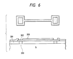
- Samples were further treated from the samples of Example 1 to evaluate the stress migration durability. More specifically, in each of these samples, Al (thickness: 0.5 ⁇ m) was patterned to have a width of 0.8 ⁇ m on an insulating film, and a silicon nitride film was deposited thereon (Fig. 6). Each sample was left to stand at a temperature of 200°C, and a time required for Al film disconnection was measured.
- Fig. 6 shows each sample.
- the sample comprises an Si substrate 200, a silicon oxide film 201 having an opening, an Al film 202, and a silicon oxide film 203.
- Characteristics of an interface between the Al film obtained by selective deposition and the Al film obtained by non-selective deposition were good. It may be assumed that impurities are not mixed in the resultant film due to a high deposition rate.
- Al was selectively deposited on only the Si-exposed portions to have the same thickness as that of SiO2 in the first Al deposition process.
- Al was deposited on both the Al film deposited in the first Al film deposition process and the SiO2 surface at the same deposition rate.
- the Al film selectively formed on Si and the Al film deposited on SiO2 upon surface modification had identical film quality in resistivity, reflectance, and hillock generation density upon annealing.
- the substrate surface upon cleaning with HF in the pre-treatment was set to be terminated with the H and F atoms.
- a sample which was not finally sufficiently cleaned with water (T 0 minutes) had a thicker spontaneous oxide film on Si than those of other samples, thus interrupting monocrystalline growth.
- T 0 minutes
- the final cleaning with water appropriately ranged from 3 to 15 minutes, only F atom bonds were eliminated, and the H atoms which contributed to the reaction tended to be terminated, thereby selectively growing Al.
- Square contact holes each having a side of 1 ⁇ m were formed in each monocrystalline wafer such that the surface of the wafer had an aspect ratio of 1 or more, thereby obtaining 12 wafers.
- the number of contact holes in each wafer was 800,000.
- the number of wiring patterns free from defects is defined as M.
- Example 7 Samples (two samples for each sample No.) formed in Example 7 were prepared. These samples were heated in an N2 atmosphere at 600°C, and most of the adsorbed hydrogen atoms were eliminated.
- Example 7 Samples as in Example 7 were prepared, and the partial pressure of DMAH was changed under the same conditions as in Example 7, thereby evaluating the yield.
- a high-quality film containing Al as a major constituent which has excellent stress migration durability can be formed at a high deposition rate.
- Thin polycrystalline tungsten (W) films were formed in the respective contact holes by a selective deposition method using WF6 by following the same procedures as in Example 1.
- Example 1 The chemical surface-treatment as in Example 1 was performed to terminate uncombined bonds of the W film surface with hydrogen atoms. Thereafter, the partial pressure of DMAH was changed as in Example 1 to form Al films. The characteristics of the resultant samples were better than those in Examples 1 and 5. There can be provided a highly reliable semiconductor device wherein a probability for producing a sample having excellent migration durability is high and reproducibility is good.
- adhesion strength can be improved when an Al wiring layer is connected to a non-monocrystalline electrode such as a gate electrode, a barrier metal electrode, and a polysilicon electrode, a deposition film having high reliability and good reproducibility can be formed.
- the present invention by controlling a plasma, reliability can be improved when an Al film is deposited on the non-electron donor surface.
- the partial pressure of an organic metal is controlled to increase a deposition rate of the Al film.
Landscapes
- Chemical & Material Sciences (AREA)
- General Chemical & Material Sciences (AREA)
- Chemical Kinetics & Catalysis (AREA)
- Engineering & Computer Science (AREA)
- Materials Engineering (AREA)
- Mechanical Engineering (AREA)
- Metallurgy (AREA)
- Organic Chemistry (AREA)
- Internal Circuitry In Semiconductor Integrated Circuit Devices (AREA)
- Electrodes Of Semiconductors (AREA)
- Chemical Vapour Deposition (AREA)
Applications Claiming Priority (4)
| Application Number | Priority Date | Filing Date | Title |
|---|---|---|---|
| JP13395/91 | 1991-02-04 | ||
| JP1339891 | 1991-02-04 | ||
| JP1339591 | 1991-02-04 | ||
| JP13398/91 | 1991-02-04 |
Publications (1)
| Publication Number | Publication Date |
|---|---|
| EP0498580A1 true EP0498580A1 (fr) | 1992-08-12 |
Family
ID=26349182
Family Applications (1)
| Application Number | Title | Priority Date | Filing Date |
|---|---|---|---|
| EP92300853A Ceased EP0498580A1 (fr) | 1991-02-04 | 1992-01-31 | Méthode dépôt d'un film métallique contenant de l'aluminium en utilisant un halide d'alkylaluminium |
Country Status (2)
| Country | Link |
|---|---|
| US (1) | US5492734A (fr) |
| EP (1) | EP0498580A1 (fr) |
Cited By (4)
| Publication number | Priority date | Publication date | Assignee | Title |
|---|---|---|---|---|
| US10825912B2 (en) | 2016-09-22 | 2020-11-03 | Iqe Plc | Integrated epitaxial metal electrodes |
| WO2020246995A1 (fr) * | 2019-06-06 | 2020-12-10 | Iqe Plc | Électrodes métalliques épitaxiales intégrées pour dispositifs modifiés |
| CN112309831A (zh) * | 2019-07-26 | 2021-02-02 | 三星电子株式会社 | 形成氧化物膜的方法、制造半导体器件的方法、形成介电膜的方法和半导体器件 |
| US11495670B2 (en) | 2016-09-22 | 2022-11-08 | Iqe Plc | Integrated epitaxial metal electrodes |
Families Citing this family (19)
| Publication number | Priority date | Publication date | Assignee | Title |
|---|---|---|---|---|
| JPH1081971A (ja) | 1996-07-10 | 1998-03-31 | Suzuki Motor Corp | 高分子基材へのプラズマCVDによるSiC薄膜形成方法及び装置 |
| KR100226751B1 (ko) * | 1997-04-10 | 1999-10-15 | 구본준 | 반도체 소자의 금속 배선 형성방법 |
| JP3529989B2 (ja) * | 1997-09-12 | 2004-05-24 | 株式会社東芝 | 成膜方法及び半導体装置の製造方法 |
| US6319566B1 (en) | 1997-11-12 | 2001-11-20 | John C. Polanyi | Method of molecular-scale pattern imprinting at surfaces |
| US6156393A (en) * | 1997-11-12 | 2000-12-05 | John C. Polanyi | Method of molecular-scale pattern imprinting at surfaces |
| US6878417B2 (en) * | 1997-11-12 | 2005-04-12 | John C. Polanyi | Method of molecular-scale pattern imprinting at surfaces |
| US6277744B1 (en) | 2000-01-21 | 2001-08-21 | Advanced Micro Devices, Inc. | Two-level silane nucleation for blanket tungsten deposition |
| US6284636B1 (en) | 2000-01-21 | 2001-09-04 | Advanced Micro Devices, Inc. | Tungsten gate method and apparatus |
| US6274472B1 (en) * | 2000-01-21 | 2001-08-14 | Advanced Micro Devices, Inc. | Tungsten interconnect method |
| US6921722B2 (en) * | 2000-05-30 | 2005-07-26 | Ebara Corporation | Coating, modification and etching of substrate surface with particle beam irradiation of the same |
| US6660083B2 (en) * | 2001-03-30 | 2003-12-09 | Technologies And Devices International, Inc. | Method of epitaxially growing device structures with submicron group III nitride layers utilizing HVPE |
| US20070032046A1 (en) * | 2001-07-06 | 2007-02-08 | Dmitriev Vladimir A | Method for simultaneously producing multiple wafers during a single epitaxial growth run and semiconductor structure grown thereby |
| US20060011135A1 (en) * | 2001-07-06 | 2006-01-19 | Dmitriev Vladimir A | HVPE apparatus for simultaneously producing multiple wafers during a single epitaxial growth run |
| US6613143B1 (en) * | 2001-07-06 | 2003-09-02 | Technologies And Devices International, Inc. | Method for fabricating bulk GaN single crystals |
| US7501023B2 (en) * | 2001-07-06 | 2009-03-10 | Technologies And Devices, International, Inc. | Method and apparatus for fabricating crack-free Group III nitride semiconductor materials |
| US6774012B1 (en) * | 2002-11-08 | 2004-08-10 | Cypress Semiconductor Corp. | Furnace system and method for selectively oxidizing a sidewall surface of a gate conductor by oxidizing a silicon sidewall in lieu of a refractory metal sidewall |
| US8252640B1 (en) | 2006-11-02 | 2012-08-28 | Kapre Ravindra M | Polycrystalline silicon activation RTA |
| JP5562413B2 (ja) * | 2010-04-22 | 2014-07-30 | 京セラ株式会社 | 薄膜太陽電池の製造方法 |
| US9224607B2 (en) | 2013-09-18 | 2015-12-29 | Globalfoundries Inc. | Dual epitaxy region integration |
Citations (5)
| Publication number | Priority date | Publication date | Assignee | Title |
|---|---|---|---|---|
| GB2041983A (en) * | 1978-11-09 | 1980-09-17 | Standard Telephones Cables Ltd | Metallising semiconductor devices |
| WO1986006756A1 (fr) * | 1985-05-03 | 1986-11-20 | American Telephone & Telegraph Company | Procede de fabrication d'un dispositif comprenant une couche de circuit en aluminium |
| EP0417997A1 (fr) * | 1989-09-09 | 1991-03-20 | Canon Kabushiki Kaisha | Procédé de déposition d'un film métallique contenant de l'aluminium comme composé principal par utilisation d'un hydride d'aluminium alkylé |
| EP0420595A2 (fr) * | 1989-09-26 | 1991-04-03 | Canon Kabushiki Kaisha | Formation d'un film déposé sélectivement utilisant de l'hydrure d'alkyl-aluminium double de métal |
| EP0425084A1 (fr) * | 1989-09-09 | 1991-05-02 | Canon Kabushiki Kaisha | Procédé de déposition d'un film utilisant un hydride d'aluminium alkylé |
Family Cites Families (10)
| Publication number | Priority date | Publication date | Assignee | Title |
|---|---|---|---|---|
| GB882214A (en) * | 1958-06-16 | 1961-11-15 | Union Carbide Corp | Apparatus and method for gas plating with aluminium |
| JPS62142778A (ja) * | 1985-12-18 | 1987-06-26 | Canon Inc | 堆積膜形成法 |
| EP0255454A3 (fr) * | 1986-07-26 | 1991-11-21 | Nihon Shinku Gijutsu Kabushiki Kaisha | Dispositif pour déposition chimique en phase vapeur |
| JPS63239195A (ja) * | 1987-03-27 | 1988-10-05 | Japan Synthetic Rubber Co Ltd | ダイヤモンド状物質の製造方法 |
| JPH01283374A (ja) * | 1988-05-10 | 1989-11-14 | Nec Corp | アルミニウム薄膜の堆積方法 |
| EP0420594B1 (fr) * | 1989-09-26 | 1996-04-17 | Canon Kabushiki Kaisha | Procédé de formation d'un film en métal déposé avec de l'aluminium comme composant principal par utilisation d'hydrure double de métal alcalin et d'aluminium |
| JP2726118B2 (ja) * | 1989-09-26 | 1998-03-11 | キヤノン株式会社 | 堆積膜形成法 |
| EP0448223B1 (fr) * | 1990-02-19 | 1996-06-26 | Canon Kabushiki Kaisha | Procédé de formation d'un film de métal déposé avec de l'aluminium comme composant principal utilisant d'hydrure d'alkyl aluminium |
| DE69130595T2 (de) * | 1990-07-06 | 1999-05-27 | Tsubouchi, Kazuo, Sendai, Miyagi | Verfahren zur Herstellung einer Metallschicht |
| JPH04221822A (ja) * | 1990-12-21 | 1992-08-12 | Kazuo Tsubouchi | 堆積膜形成法 |
-
1992
- 1992-01-31 EP EP92300853A patent/EP0498580A1/fr not_active Ceased
-
1994
- 1994-06-17 US US08/261,883 patent/US5492734A/en not_active Expired - Fee Related
Patent Citations (5)
| Publication number | Priority date | Publication date | Assignee | Title |
|---|---|---|---|---|
| GB2041983A (en) * | 1978-11-09 | 1980-09-17 | Standard Telephones Cables Ltd | Metallising semiconductor devices |
| WO1986006756A1 (fr) * | 1985-05-03 | 1986-11-20 | American Telephone & Telegraph Company | Procede de fabrication d'un dispositif comprenant une couche de circuit en aluminium |
| EP0417997A1 (fr) * | 1989-09-09 | 1991-03-20 | Canon Kabushiki Kaisha | Procédé de déposition d'un film métallique contenant de l'aluminium comme composé principal par utilisation d'un hydride d'aluminium alkylé |
| EP0425084A1 (fr) * | 1989-09-09 | 1991-05-02 | Canon Kabushiki Kaisha | Procédé de déposition d'un film utilisant un hydride d'aluminium alkylé |
| EP0420595A2 (fr) * | 1989-09-26 | 1991-04-03 | Canon Kabushiki Kaisha | Formation d'un film déposé sélectivement utilisant de l'hydrure d'alkyl-aluminium double de métal |
Non-Patent Citations (6)
| Title |
|---|
| APPLIED PHYSICS LETTERS. vol. 56, no. 7, 12 February 1990, NEW YORK US pages 656 - 658; G.S. HIGASHI ET AL.: 'Ideal hydrogen termination of the Si(111) surface' * |
| APPLIED PHYSICS LETTERS. vol. 57, no. 12, 17 September 1990, NEW YORK US pages 1221 - 1223; KAZUO TSUBOUCHI ET AL.: 'Complete planarization of via holes with aluminium by selective and non selective chemical vapor deposition' * |
| JOURNAL OF THE ELECTROCHEMICAL SOCIETY. vol. 137, no. 10, October 1990, MANCHESTER, NEW HAMPSHIRE US pages 3287 - 3291; SYLVIA D. HOSSAIN ET AL.: 'Removal of surface organic contaminants during thermal oxidation of Silicon' * |
| PATENT ABSTRACTS OF JAPAN vol. 13, no. 42 (C-564)30 January 1989 & JP-A-63 239 195 ( JAPAN SYNTHETIC RUBBER CO. LTD. ) 5 October 1988 * |
| SYMPOSIUM ON VLSI TECHNOLOGY-DIGEST OF TECHNICAL PAPERS 4 June 1990, HONOLULU pages 5 - 6; K.TSUBOUCHI ET AL.: 'Selective and non selective deposition of Aluminium by LPCVD using DMAH and microregion observation of single crystal Aluminium with scanning u-RHEED microscope' * |
| THIN SOLID FILMS. vol. 107, no. 1, September 1983, LAUSANNE CH pages 3 - 19; JOHN A. THORNTON: 'Plasma-assisted deposition processes: Theory, mechanisms and applications' * |
Cited By (4)
| Publication number | Priority date | Publication date | Assignee | Title |
|---|---|---|---|---|
| US10825912B2 (en) | 2016-09-22 | 2020-11-03 | Iqe Plc | Integrated epitaxial metal electrodes |
| US11495670B2 (en) | 2016-09-22 | 2022-11-08 | Iqe Plc | Integrated epitaxial metal electrodes |
| WO2020246995A1 (fr) * | 2019-06-06 | 2020-12-10 | Iqe Plc | Électrodes métalliques épitaxiales intégrées pour dispositifs modifiés |
| CN112309831A (zh) * | 2019-07-26 | 2021-02-02 | 三星电子株式会社 | 形成氧化物膜的方法、制造半导体器件的方法、形成介电膜的方法和半导体器件 |
Also Published As
| Publication number | Publication date |
|---|---|
| US5492734A (en) | 1996-02-20 |
Similar Documents
| Publication | Publication Date | Title |
|---|---|---|
| US5492734A (en) | Method of forming deposition film | |
| EP0493002B1 (fr) | Procédé de formation d'un film déposé | |
| EP0420595B1 (fr) | Formation d'un film déposé sélectivement utilisant de l'hydrure d'alkyl-aluminium double de métal | |
| US6258174B1 (en) | Gas supplying apparatus | |
| US5747384A (en) | Process of forming a refractory metal thin film | |
| EP0425084B1 (fr) | Procédé de déposition d'un film utilisant un hydride d'aluminium alkylé | |
| EP0216157B1 (fr) | Méthode pour déposer des régions métalliques de contact sur un substrat de silicium | |
| EP0909985A1 (fr) | Méthode de traitement et appareillage photolithographique | |
| US20040161535A1 (en) | Method of forming silicon carbide films | |
| EP0420594B1 (fr) | Procédé de formation d'un film en métal déposé avec de l'aluminium comme composant principal par utilisation d'hydrure double de métal alcalin et d'aluminium | |
| JP2726118B2 (ja) | 堆積膜形成法 | |
| EP0539948B1 (fr) | Appareillage et procédé pour fabriquer des films métalliques | |
| EP0420597A2 (fr) | Procédé pour la formation d'un film déposé en utilisant de l'alkyle de l'hydrure d'aluminium et procédé de fabrication d'un dispositif semi-conducteur | |
| EP0420589B1 (fr) | Procédé pour la formation d'un film déposé et procédé de fabrication d'un dispositif semi-conducteur | |
| JPS6248752B2 (fr) | ||
| JP3176088B2 (ja) | 堆積膜形成法 | |
| EP0417997B1 (fr) | Procédé de déposition d'un film métallique contenant de l'aluminium comme composé principal par utilisation d'un hydride d'aluminium alkylé | |
| JP2945886B2 (ja) | 半導体集積回路装置用配線構造の製造法 | |
| JP2670152B2 (ja) | 堆積膜形成法 | |
| JP3029679B2 (ja) | 金属膜形成法および気相化学反応装置 | |
| JPH03110838A (ja) | 堆積膜形成法 | |
| JPH0559552A (ja) | 堆積膜形成法 | |
| JP2781219B2 (ja) | 堆積膜形成法 | |
| JP2721020B2 (ja) | 堆積膜形成法 | |
| EP0345400A1 (fr) | CVD sélectif pour fabrication de dispositifs à semi-conducteurs |
Legal Events
| Date | Code | Title | Description |
|---|---|---|---|
| PUAI | Public reference made under article 153(3) epc to a published international application that has entered the european phase |
Free format text: ORIGINAL CODE: 0009012 |
|
| AK | Designated contracting states |
Kind code of ref document: A1 Designated state(s): DE FR GB |
|
| 17P | Request for examination filed |
Effective date: 19921228 |
|
| 17Q | First examination report despatched |
Effective date: 19930705 |
|
| 18R | Application refused |
Effective date: 19961129 |