EP0501361A1 - Corps d'interconnexion électrique et procédé de sa fabrication - Google Patents
Corps d'interconnexion électrique et procédé de sa fabrication Download PDFInfo
- Publication number
- EP0501361A1 EP0501361A1 EP92103028A EP92103028A EP0501361A1 EP 0501361 A1 EP0501361 A1 EP 0501361A1 EP 92103028 A EP92103028 A EP 92103028A EP 92103028 A EP92103028 A EP 92103028A EP 0501361 A1 EP0501361 A1 EP 0501361A1
- Authority
- EP
- European Patent Office
- Prior art keywords
- electrically conductive
- apertures
- photosensitive resin
- holding member
- conductive material
- Prior art date
- Legal status (The legal status is an assumption and is not a legal conclusion. Google has not performed a legal analysis and makes no representation as to the accuracy of the status listed.)
- Granted
Links
Images


Classifications
-
- H—ELECTRICITY
- H10—SEMICONDUCTOR DEVICES; ELECTRIC SOLID-STATE DEVICES NOT OTHERWISE PROVIDED FOR
- H10W—GENERIC PACKAGES, INTERCONNECTIONS, CONNECTORS OR OTHER CONSTRUCTIONAL DETAILS OF DEVICES COVERED BY CLASS H10
- H10W70/00—Package substrates; Interposers; Redistribution layers [RDL]
- H10W70/01—Manufacture or treatment
- H10W70/05—Manufacture or treatment of insulating or insulated package substrates, or of interposers, or of redistribution layers
- H10W70/095—Manufacture or treatment of insulating or insulated package substrates, or of interposers, or of redistribution layers of vias therein
-
- H—ELECTRICITY
- H10—SEMICONDUCTOR DEVICES; ELECTRIC SOLID-STATE DEVICES NOT OTHERWISE PROVIDED FOR
- H10W—GENERIC PACKAGES, INTERCONNECTIONS, CONNECTORS OR OTHER CONSTRUCTIONAL DETAILS OF DEVICES COVERED BY CLASS H10
- H10W70/00—Package substrates; Interposers; Redistribution layers [RDL]
- H10W70/60—Insulating or insulated package substrates; Interposers; Redistribution layers
- H10W70/62—Insulating or insulated package substrates; Interposers; Redistribution layers characterised by their interconnections
- H10W70/63—Vias, e.g. via plugs
- H10W70/635—Through-vias
-
- H—ELECTRICITY
- H10—SEMICONDUCTOR DEVICES; ELECTRIC SOLID-STATE DEVICES NOT OTHERWISE PROVIDED FOR
- H10W—GENERIC PACKAGES, INTERCONNECTIONS, CONNECTORS OR OTHER CONSTRUCTIONAL DETAILS OF DEVICES COVERED BY CLASS H10
- H10W72/00—Interconnections or connectors in packages
- H10W72/071—Connecting or disconnecting
- H10W72/072—Connecting or disconnecting of bump connectors
- H10W72/07251—Connecting or disconnecting of bump connectors characterised by changes in properties of the bump connectors during connecting
-
- H—ELECTRICITY
- H10—SEMICONDUCTOR DEVICES; ELECTRIC SOLID-STATE DEVICES NOT OTHERWISE PROVIDED FOR
- H10W—GENERIC PACKAGES, INTERCONNECTIONS, CONNECTORS OR OTHER CONSTRUCTIONAL DETAILS OF DEVICES COVERED BY CLASS H10
- H10W72/00—Interconnections or connectors in packages
- H10W72/20—Bump connectors, e.g. solder bumps or copper pillars; Dummy bumps; Thermal bumps
-
- Y—GENERAL TAGGING OF NEW TECHNOLOGICAL DEVELOPMENTS; GENERAL TAGGING OF CROSS-SECTIONAL TECHNOLOGIES SPANNING OVER SEVERAL SECTIONS OF THE IPC; TECHNICAL SUBJECTS COVERED BY FORMER USPC CROSS-REFERENCE ART COLLECTIONS [XRACs] AND DIGESTS
- Y10—TECHNICAL SUBJECTS COVERED BY FORMER USPC
- Y10T—TECHNICAL SUBJECTS COVERED BY FORMER US CLASSIFICATION
- Y10T29/00—Metal working
- Y10T29/49—Method of mechanical manufacture
- Y10T29/49002—Electrical device making
- Y10T29/49117—Conductor or circuit manufacturing
- Y10T29/49124—On flat or curved insulated base, e.g., printed circuit, etc.
- Y10T29/49155—Manufacturing circuit on or in base
- Y10T29/49158—Manufacturing circuit on or in base with molding of insulated base
-
- Y—GENERAL TAGGING OF NEW TECHNOLOGICAL DEVELOPMENTS; GENERAL TAGGING OF CROSS-SECTIONAL TECHNOLOGIES SPANNING OVER SEVERAL SECTIONS OF THE IPC; TECHNICAL SUBJECTS COVERED BY FORMER USPC CROSS-REFERENCE ART COLLECTIONS [XRACs] AND DIGESTS
- Y10—TECHNICAL SUBJECTS COVERED BY FORMER USPC
- Y10T—TECHNICAL SUBJECTS COVERED BY FORMER US CLASSIFICATION
- Y10T29/00—Metal working
- Y10T29/49—Method of mechanical manufacture
- Y10T29/49002—Electrical device making
- Y10T29/49117—Conductor or circuit manufacturing
- Y10T29/49124—On flat or curved insulated base, e.g., printed circuit, etc.
- Y10T29/49155—Manufacturing circuit on or in base
- Y10T29/49165—Manufacturing circuit on or in base by forming conductive walled aperture in base
-
- Y—GENERAL TAGGING OF NEW TECHNOLOGICAL DEVELOPMENTS; GENERAL TAGGING OF CROSS-SECTIONAL TECHNOLOGIES SPANNING OVER SEVERAL SECTIONS OF THE IPC; TECHNICAL SUBJECTS COVERED BY FORMER USPC CROSS-REFERENCE ART COLLECTIONS [XRACs] AND DIGESTS
- Y10—TECHNICAL SUBJECTS COVERED BY FORMER USPC
- Y10T—TECHNICAL SUBJECTS COVERED BY FORMER US CLASSIFICATION
- Y10T29/00—Metal working
- Y10T29/49—Method of mechanical manufacture
- Y10T29/4981—Utilizing transitory attached element or associated separate material
- Y10T29/49812—Temporary protective coating, impregnation, or cast layer
Definitions
- This invention relates to an electrical connecting member for use when electric circuit parts are to be electrically connected together and a method of manufacturing the same.
- FIG 1 of the accompanying drawings is a schematic view showing the electrical connection of electric circuit parts using such an electrical connecting member.
- the reference numeral 31 designates an electrical connecting member
- the reference numerals 32 and 33 denote electric circuit parts to be connected together.
- the electrical connecting member 31 comprises a plurality of electrically conductive members 34 formed of a metal or an alloy, electrically insulated from one another and provided in a holding member 35 formed of an electrically insulative material, and one end 38 of each electrically conductive member 34 is exposed on the side of one electric circuit part 32 and the other end 39 of each electrically conductive member 34 is exposed on the side of the other electric circuit part 33 ( Figure 1(a)).
- the connecting portion 36 of said one electric circuit part 32 and one end 38 of each electrically conductive member 34 exposed on the side of the electric circuit part 32 are made into an alloy to thereby join the two together, and the connecting portion 37 of said other electric circuit part 33 and the other end 39 of each electrically conductive member 34 exposed on the side of the electric circuit part 33 are made into an alloy to thereby join the two together and thus, the electric circuit parts 32 and 33 are electrically connected together (Figure 1B).
- a base body 51 comprising a metal sheet such a copper plate is first prepared, and negative-type photosensitive resin 52 is applied onto this base body 51 by a spin coater, and pre-baking is effected at a temperature of about 100°C ( Figure 2A).
- Light is applied to the photosensitive resin 52 through a photomask (not shown) forming a predetermined pattern, whereafter developing liquid is injected to the photosensitive resin or the photosensitive resin is immersed in developing liquid to thereby effect development.
- the photosensitive resin 52 remains on the portions exposed to light and the photosensitive resin 52 is removed from the portions not exposed to light by the developing process, whereby a plurality of apertures 53 are formed (Figure 2B).
- FIG. 3 of the accompanying drawings is a schematic view showing the state of the electroplating step in such a process.
- the reference numeral 61 designates a plating vessel.
- a mesh-like anode 62 is disposed in the lower portion of the plating vessel 61, and a cathode 63 is disposed in the upper portion of the plating vessel in opposed relationship with the anode 62.
- An intermediate member 64 as shown in Figure 2C is placed on the cathode 63, and plating liquid 65 low in gold concentration is caused to flow at a low speed from below toward above to thereby apply so-called strike plating and coat the surfaces of the recesses 54 with gold, whereafter so-called thickening plating is applied by the use of plating liquid high in gold concentration to thereby fill the recesses 54 and apertures 53 with gold, thus forming electrically conductive members 34.
- the gold 55 constitutes the electrically conductive members 34 and the photosensitive resin 52 constitutes the holding member 35.
- the thickness of the photosensitive resin 52 is about 10 ⁇ m
- the diameter and pitch of the apertures 53 are about 20 ⁇ m and about 40 ⁇ m, respectively
- the amounts of protrusion of the electrically conductive members 34 on the obverse and reverse are of the order of several ⁇ m.
- the reliability of the above-described electrical connecting member is achieved by bumps of a uniform shape and uniform height of protrusion being provided.
- the photosensitive resin 52 becomes liable to flow with the developing liquid or dissolve in the process of leaving the photosensitive resin 52 as it is after the developing step or in the process of curing the photosensitive resin 52 after the developing step. Accordingly, as shown in Figure 4 of the accompanying drawings which shows the state before the formation of the recesses 54 on an enlarged scale, the formed apertures 53 are tapered at 53a or the pattern thereof gets out of shape, and the shape of the apertures 53 becomes irregular. This leads to the problem that in the manufactured electrical connecting member 31, the shape of the electrically conductive members is not stable.
- the occurrence of the resin-like residue becomes remarkable when the aspect ratio (film thickness/diameter of opening) of the apertures 53 is great, or when the exposure and developing conditions are inappropriate, or when diffracted light and/or reflected light irradiates the portions of the photosensitive resin which should not be exposed to the light.
- the presence of such resin-like residue has led to the problem that it hampers the exposure of the surface of the metal sheet 51 at the bottom of the apertures 53 and as shown in Figure 5B, the shape of the recesses 54 is made irregular in the process of etching the surface of the metal sheet 51 and as shown in Figure 5C, the shape of bumps is not constant and the electrical characteristic is not stable.
- the shape (e.g. diameter and amount of protrusion) of the gold bumps becomes non-uniform depending on the gold electroplating conditions, for example, the Reynolds number of liquid flow imparted to the plating liquid, the current density, the amount of a plating liquid additive etc.
- the amount of plating deposition is greater in the central portion than in the marginal portion under the influence of the current density distribution and therefore, in an electrical connecting member, the amount of protrusion of electrically conductive members present in the central portion becomes greater than the amount of protrusion of electrically conductive members present in the marginal portion and thus, it is not easy to make the diameter of protrusion and the height of protrusion of the electrically conductive members uniform.
- Figure 6 of the accompanying drawings is a plan view of an electrical connecting member having four electrically conductive members 34
- Figure 7 of the accompanying drawings is a plan view of an electrical connecting member having seven electrically conductive members 34.
- FIG. 6 wherein four electrically conductive members 34 are located at the verteces of a lozenge, the amount of protrusion of the two electrically conductive members 34 at the verteces the diagonal of which is shorter is greater than that of the other two electrically conductive members 34.
- Figure 7 wherein six electrically conductive members 34 are disposed so as to surround an electrically conductive member 34, the central one is greater in the amount of protrusion than the other six ones.
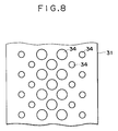
- Figure 8 of the accompanying drawings is a fragmentary plan view of an electrical connecting member 31 forming a pattern in which a number of rows of seven electrically conductive members 34 each are disposed. In each row, the amount of protrusion is smaller in the marginal portion than in the central portion.
- the forming methods as described above suffer from such problems as will be described below.
- the removing step is cumbersome, and when the ground metal layer is removed in its liquid phase, etching liquid remains and this remaining liquid is liable to be mixed with the gold plating liquid to cause a bad shape.
- the area of contact with the ground metal layer is small and therefore the intimate contact property is deficient and thus, this method is liable to cause a reduction in the strength of the protrusions during boding.
- the method of repeating the photolithography step and the gold plating method generally requires a long time as the steps, and the alignment in the photolithography step is difficult, and this leads to the problem that the control of the height of the gold plating in each step is difficult.
- Figures 1A and 1B are schematic views showing an example of the use of an electrical connecting member.
- Figures 2A - 2E are schematic cross-sectional views showing the steps of a prior-art manufacturing method.
- Figure 3 is a schematic view showing a state in which the plating process is carried out.
- Figure 4 is a schematic cross-sectional view showing a part of the manufacturing step for illustrating problems peculiar to the prior-art manufacturing method.
- Figures 5A - 5C are schematic cross-sectional views showing cases where the prior-art manufacturing method is inconvenient.
- Figure 6 is a schematic view for illustrating problems in the prior-art manufacturing method.
- Figure 7 is a schematic view for illustrating problems in the prior-art manufacturing method.
- Figure 8 is a schematic view for illustrating problems in the prior-art manufacturing method.
- Figures 9A - 9E are schematic cross-sectional views showing the essential steps of a manufacturing method according to an embodiment of the present invention.
- Figure 10 is a schematic view showing a developing mode in the embodiment of the present invention.
- Figures 11A and 11B are fragmentary enlarged cross-sectional views showing the states during the injection of developing liquid and during the stoppage of the injection of the developing liquid, respectively.
- Figure 12 is a time chart showing the patterns during the injection of the developing liquid and during the stoppage of the injection of the developing liquid, respectively.
- Figure 13 is a schematic view showing another developing mode used in the embodiment of the present invention.
- Figure 14 is a fragmentary enlarged cross-sectional view of the surface of a copper plate 1 shown in Figure 13.
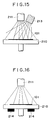
- Figure 15 is a schematic view showing still another developing mode used in the embodiment of the present invention.
- Figure 16 is a schematic view showing yet still another developing mode used in the embodiment of the present invention.
- Figure 17 is a schematic view showing a further developing mode used in the embodiment of the present invention.
- Figure 18 is a graph showing an example of the mode of a heated atmosphere and/or a negative pressure atmosphere in the manufacturing method according to the embodiment of the present invention.
- Figure 19 is a graph showing another example of the mode of a heated atmosphere and/or a negative pressure atmosphere in the manufacturing method according to the embodiment of the present invention.
- Figure 20 is a graph showing still another example of the mode of a heated atmosphere and/or a negative pressure atmosphere in the manufacturing method according to the embodiment of the present invention.
- Figures 21A - 21C are schematic cross-sectional views showing the shape of a gold protrusion formed.
- Figure 22 is a schematic plan view of electrically conductive members in an electrical connecting member manufactured by a prior-art manufacturing method.
- Figure 23 is a schematic plan view of electrically conductive members in an electrical connecting member manufactured by a manufacturing method according to the embodiment of the present invention.
- Figure 24 is a schematic plan view of electrically conductive members in an electrical connecting member manufactured by the prior-art manufacturing method.
- Figure 25 is a schematic plan view of electrically conductive members in an electrical connecting member manufactured by the manufacturing method according to the embodiment of the present invention.
- Figure 26 is a schematic plan view of electrically conductive members in an electrical connecting member manufactured by the prior-art manufacturing method.
- Figure 27 is a schematic plan view of electrically conductive members in an electrical connecting member manufactured by the manufacturing method according to the embodiment of the present invention.
- FIGS 9A - 9B are schematic cross-sectional views showing the manufacturing steps according to an embodiment of the present invention.
- Negative type polyimide resin 102 which is photosensitive resin is first applied onto a copper plate 101 which is a base body by a spin coater, and then is pre-baked, whereafter light (not shown) is applied to the polyimide resin 102 through a photomask 103 forming a predetermined pattern ( Figure 9A).
- the film thickness of the applied polyimide resin 102 is made greater than the desired film thickness of a holding member in an electrical connecting member to be manufactured, with a decrease by the curing and shrinkage of the resin taken into account.
- developing liquid is injected to the polyimide resin or the polyimide resin is immersed in developing liquid to thereby effect development.
- FIG 10 is a schematic view showing a developing mode in the present embodiment.
- the copper plate 101 which is the base body (together with the photosensitive resin 102 exposed to light) is placed on a turn table 210, and developing liquid is intermittently injected to the surface of the copper plate 101 from an injection nozzle 211 for the developing liquid disposed above and in opposed relationship with the turn table 210 while the turn table 210 is continuously rotated at a predetermined speed, whereby development is effected.
- Figure 11A is a fragmentary enlarged view showing the state during the injection of the developing liquid
- Figure 11B is a fragmentary enlarged view showing the state during the stoppage of the injection of the developing liquid.
- the developing liquid collects and stagnates in apertures 104 formed by development, but in the injection stopping process of the developing liquid, the developing liquid is discharged out of the apertures 104 with residue by a centrifugal force and development is expedited by the injection of fresh developing liquid.
- FIG. 12 which is a time chart showing the injection timing of the developing liquid
- the horizontal axis represents time and the vertical axis represents the injection state and injection stopped state of the developing liquid.
- the injection time and the injection stoppage time are set as required to thereby effect the injection and the stoppage alternately.
- Figure 13 is a schematic view showing another developing mode used in the present embodiment
- Figure 14 is a fragmentary enlarged cross-sectional view of the surface of the copper plate 101.
- the upper plate 101 is placed on the turn table 210 rotated at a predetermined speed, and the developing liquid is continuously injected from the injection nozzle 211 disposed above and in opposed relationship with the turn table, and an air nozzle 212 is disposed sideways of the turn table 210 in proximity to and in parallelism to the surface of the turn table 210, and air is injected along the surface of the copper plate 101 from the air nozzle 212 with pressure of the order of 0-10 kgf/cm2.
- negative pressure is created in the apertures 104 by the sucking action of air and the developing liquid and developing residue in the apertures 104 are sucked and removed.
- the developing liquid is continuously or intermittently injected from the injection nozzle 211.
- Figure 15 is a schematic view showing still another developing mode used in the present embodiment.
- An air nozzle 213 is somewhat obliquely disposed sideways of the injection nozzle 211 for the developing liquid.
- the developing liquid is continuously or intermittently injected from the injection nozzle 211 for the developing liquid.
- FIG 16 is a schematic view showing yet still another developing mode used in the present embodiment.
- Ultrasonic vibrators 214 of e.g. 20 kHz to 10 MHz as a single or plural kinds of frequencies are attached to the underside of the turn table 210.
- the turn table 210 and the copper plate 101 are vibrated at a high speed, whereby the circulation of the developing liquid in the apertures is expedited and the removal of residue can be accomplished effectively.
- the developing liquid is continuously or intermittently injected from the injection nozzle 211 for the developing liquid.
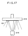
- FIG 17 is a schematic view showing a further developing mode used in the present embodiment.
- the turn table 210 is provided so as to face downwardly and the copper plate 101 is fixed to the underside thereof by a fixture, not shown, and an injection nozzle 215 for developing liquid is disposed below and in opposed relationship with the turn table 210.
- the developing liquid injected into the apertures 104 does not collect in the apertures 104 but can be automatically discharged with residue, and the circulation efficiency of the developing liquid in the apertures 104 is improved.
- the developing liquid is continuously or intermittently injected from the injection nozzle 215.
- the polyimide resin 102 remains in the portions exposed to light and the polyimide resin 102 is removed from the portions not exposed to light by the developing process, whereby a plurality of apertures 104 are formed in the polyimide resin 102 ( Figure 9B).
- the developing liquid infiltrates into the polyimide resin 102, which is thus expanded a little, and the diameter of the apertures 104 formed in the polyimide resin 102 becomes smaller than the predetermined pattern of the photomask 103 and the shape of the formed apertures 104 is not constant.
- the intermediate member 110 after the developing step is left in one or both of heated and negative pressure atmospheres for a predetermined time to thereby evaporate the developing liquid which has infiltrated into the polyimide resin 102.
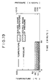
- Figure 18 shows an example of the atmosphere in this case (a case where the boiling point of the developing liquid is 200°C).
- the termination of the time for which the intermediate member is left in such an atmosphere can be judged at a point of time whereat the weight of the intermediate member 110 scarcely changes after greatly decreased by the evaporation of the developing liquid.
- the developing liquid which has infiltrated into the polyimide resin 102 is removed to thereby form a plurality of apertures 104 having a uniform pattern shape having no taper formed ( Figure 9C).
- the heating temperature is increased to 200-400°C to thereby cure the polyimide resin 102, whereafter the copper plate 101 is immersed in etching liquid to thereby effect the etching of the copper plate 101 and remove the portions of the copper plate 101 which are near the apertures 104 by etching, thereby forming in the copper plate 101 recesses 105 communicating with the apertures 104 ( Figure 9D).
- the diameter of the recesses 105 formed at this time is larger than the diameter of the apertures 104 and small than a half of the distance to the outer periphery of the adjacent aperture 104.
- the intermediate member 110 when removing the developing liquid which has infiltrated into the polyimide resin 102, the intermediate member 110 is left in the heated and negative pressure atmospheres, but alternatively, the intermediate member may be left in one of the heated atmosphere and the negative pressure atmosphere.
- Examples of the atmosphere in such a case a case where the boiling point of the developing liquid is 200°C are shown in Figures 19 and 20.
- Figure 19 represents an example of the normal temperature and negative pressure atmosphere
- Figure 20 represents an example of the heated and increased pressure atmosphere.
- gold protrusions are formed at locations of 8 mm from the center of the rotational shaft, and gold plating liquid of sulfite line is used as gold plating liquid.
- FIGS 21A - 21C are cross-sectional views showing the shape of a gold protrusion formed.
- the reference numeral 102 designates photoresist which provides a holding member, and an opening 104 to be gold-lated is provided by the photoresist 102 of a predetermined pattern, and a gold protrusion 106 is formed in the opening 104.
- d indicates the diameter of the opening 104.
- Figure 21 The shape of the formed gold protrusion can be classified into three kinds as shown in Figure 21.
- Figure 21A shows an ideal shape forming an upwardly convex shape, and such a shape will hereinafter be referred to as A.
- Figure 21B shows a bad shape having a depression formed in the central portion of the protrusion, and such a shape will hereinafter be referred to as B.
- Figure 21C shows a bad shape having a lateral expanse formed toward the marginal portion of the protrusion, and such a shape will hereinafter be referred to as C.
- the photoresist 102 was patternized so that the diameter d of the openings 104 might be 10 ⁇ m, 15 ⁇ m, 30 ⁇ m, 50 ⁇ m, 80 ⁇ m and 100 ⁇ m, and gold protrusions 106 were formed relative to the openings 104 with the Reynolds number (N Re ) of the plating liquid as 0, 10, 30, 50, 100 and 200.
- N Re Reynolds number
- 30 ppm of Tl was added to the plating liquid, and a quantity of electricity of 25 C/cm2 was imparted with the current density as 4 mA/cm2.
- the formed gold protrusions 106 were observed by means of a scanning type electronic microscope. The result of this observation is shown in Table 1 below.
- the shape of type A becomes null in all ranges of the Reynolds number 0 to 450 and the diameter of the openings of 10 ⁇ m to 200 ⁇ m in Table 1, and the bad shapes of types B and C are created. Accordingly, from Table 1 and 2, it is seen that it is preferable that the diameter d of the openings be equal to or greater than 10 ⁇ m and equal to or less than 150 ⁇ m, the Reynolds number N Re of the plating liquid be a laminar flow equal to or greater than 50 and equal to or less than 450 and the current density be equal to or greater than 1 mA/cm2 and equal to or less than 5 mA/cm2.
- the Reynolds number N Re of the plating liquid is a laminar flow equal to or greater than 50 and equal to or less than 450 and the current density is equal to or greater than 1 mA/cm2 and equal to or less than 5 mA/cm2, experiments were further carried out about the influence of an additive added to the plating liquid.
- the quantity of Tl added to the plating liquid was varied to 0 ppm, 10 ppm, 30 ppm, 60 ppm, 90 ppm, 100 ppm, 500 ppm and 1,000 ppm to thereby form gold protrusions.
- Table 3 Quantity of Tl added (ppm) 0 10 30 60 90 100 500 1,000 C C A A A A B B
- the temperature of the plating liquid is kept at room temperature (0 - 40°C) and the flow velocity of the plating liquid and the current density are varied in conformity with the growth of plating. Not all of these conditions need be satisfied, but depending on the number and arrangement pattern of electrically conductive members in an electrical connecting member to be manufactured, the uniformization of the amount of protrusion of that electrically conductive members can be realized by a single condition or a combination of any conditions.
- the amount of protrusion of the seven electrically conductive members could also be made uniform by effecting similar adjustment by the manufacturing method of the present embodiment.
- the apertures 104 and recesses 105 are filled with gold 106 by electroplating (Figure 9D).
- the recesses 105 and apertures 104 are filled with gold 106 until bumps are formed.
- the copper plate 101 is dissolved and removed by the use of etching liquid which etches copper but does not etch gold and polyimide resin, thereby manufacturing an electrical connecting member 31 ( Figure 2E).
- the gold 106 constitutes the electrically conductive members 34 ( Figure 2E) and the polyimide resin 102 constitutes the holding member 35 ( Figure 2E).
- the polyimide resin 102 is used as photosensitive resin which provides the holding member, but use may also be made of any other photosensitive resin such as epoxy resin or silicone resin.
- the copper plate 101 is used as the base body, whereas this is not restrictive, but other metal or an alloy can also be used. However, since in the final step, only the base body is selectively removed by etching, it is necessary to make the material of the electrically conductive members 34 and the material of the base body different from each other.
- photosensitive resin such as polyimide resin is used as the holding member, whereas this is not restrictive, but use may be made of any photosensitive resin.
- photosensitive resin such as polyimide resin
- one or more of inorganic materials, metal materials and alloy materials in a desired form of powder, fiber, a plate-like body, a bar-like body, a spherical body or the like may be dispersed and contained in photosensitive resin.
- metal material and alloy material contained mention may be made of Au, Ag, Cu, Al, Be, Ca, Mg, Mo, Fe, Ni, Co, Mn, W, Cr, Nb, Zr, Ti, Ta, Zn, Sn, Pb-Sn, etc.
- ceramics such as SiO2, B2O3, Al2O3, Na2O, K2O, CaO, ZnO, BaO, PbO, Sb2O3, As2O3, La2O3, ZrO2, P2O5, TiO2, MgO, SiC, BeO, BP, BN, AlN, B4C, TaC, TiB2, CrB2, TiN, Si3N4 and Ta2O5, diamond, glass, carbon, boron, etc.
- gold is used as the material of the electrically conductive members 106, but instead of gold, use may be made of a metallic simple substance such as Cu, Ag, Be, Ca, Mg, Mo, Ni, W, Fe, Ti, In, Ta, Zn, Al, Sn or Pb-Sn, or an alloy of these.
- the cross-sectional shape of the electrically conductive members 106 can be circular, square or other shapes, but to avoid the excessive concentration of stress, rounded shapes are desirable.
- the electrically conductive members 106 need not be vertically disposed in the holding member, but may be oblique from one surface side of the holding member to the other surface side of the holding member.
- the manufacturing method of the present embodiment can expedite the circulation of the developing liquid in the apertures and effectively remove the residue in the apertures and thus, can uniformize the shape of the apertures and the exposed shape of the surface of the base body exposed in the apertures and can achieve the uniformization of the shape of the recesses formed in the base body and further the shape of the electrically conductive members, thereby achieving excellent effects such as the stabilization of the characteristic and the improved yield of product.
- the manufacturing method of the present embodiment leaves the intermediate member after the developing step in a heated atmosphere and/or a negative pressure atmosphere for a predetermined time, and heats and cure it after evaporation-removing the developing liquid which has infiltrated into photosensitive resin and therefore, can form a number of apertures each forming a predetermined shape in the photosensitive resin, thus manufacturing an electrical connecting member in which the shape of all electrically conductive members is uniform.
- the manufacturing method of the present embodiment achieves excellent effects such as the capability of manufacturing an electrical connecting member having electrically conductive members provided therein at high density, and the possibility of high-density connection of electric circuit parts.
- a bad shape resulting from a depression in the central portion of each protrusion or the lateral expanse toward the marginal portion of each protrusion can be avoided and thus, there can be formed gold protrusions of a very good shape.
- the temperature of the plating liquid, the flow velocity of the plating liquid and the current density are adjusted in the electroplating step and therefore, there can be manufactured an electrical connecting member in which the influence of the current density distribution is prevented and which has a plurality of electrically conductive members having equal amounts of protrusion provided over the whole area, and as a result, there can be achieved an excellent effect such as the capability of greatly improving the manufacturing efficiency.
- an electrical connecting member capable of connecting electric circuit parts together well and a method of manufacturing the same.
- a method of manufacturing an electrical connecting member having a holding member formed of an electrically insulative material, and a plurality of electrically conductive members provided in a mutually insulated state in the holding member, one end of each of the electrically conductive members being exposed on one surface of the holding member and the other end of each of the electrically conductive members being exposed on the other surface of the holding member includes the steps of providing photosensitive resin which provides the holding member on a base body, applying light to the photosensitive resin through a photomask forming a predetermined pattern to thereby expose the photosensitive resin to the light, developing the photosensitive resin to form a plurality of apertures in the photosensitive resin, thereby exposing the base body, leaving the photosensitive resin through which the base body has been exposed in a heated atmosphere and/or a negative pressure atmosphere for a predetermined time, etching the exposed portions of the base body to thereby form recesses communicating with the apertures filling the apertures and the recesses with an electrically conductive material which provides the electrically conductive members, and removing
Landscapes
- Manufacturing Of Electrical Connectors (AREA)
Applications Claiming Priority (12)
| Application Number | Priority Date | Filing Date | Title |
|---|---|---|---|
| JP53905/91 | 1991-02-25 | ||
| JP03053905A JP3127252B2 (ja) | 1991-02-25 | 1991-02-25 | 電気的接続部材の製造方法 |
| JP5390591 | 1991-02-25 | ||
| JP6909091A JPH04282837A (ja) | 1991-03-09 | 1991-03-09 | 金突起の形成方法 |
| JP69090/91 | 1991-03-09 | ||
| JP6909091 | 1991-03-09 | ||
| JP8759791A JPH04296483A (ja) | 1991-03-26 | 1991-03-26 | 電気的接続部材の製造方法 |
| JP87597/91 | 1991-03-26 | ||
| JP8759791 | 1991-03-26 | ||
| JP03091638A JP3108792B2 (ja) | 1991-03-28 | 1991-03-28 | 電気的接続部材の製造方法 |
| JP9163891 | 1991-03-28 | ||
| JP91638/91 | 1991-03-28 |
Publications (2)
| Publication Number | Publication Date |
|---|---|
| EP0501361A1 true EP0501361A1 (fr) | 1992-09-02 |
| EP0501361B1 EP0501361B1 (fr) | 2002-05-15 |
Family
ID=27462980
Family Applications (1)
| Application Number | Title | Priority Date | Filing Date |
|---|---|---|---|
| EP92103028A Expired - Lifetime EP0501361B1 (fr) | 1991-02-25 | 1992-02-24 | Corps d'interconnexion électrique et procédé de sa fabrication |
Country Status (3)
| Country | Link |
|---|---|
| US (1) | US5323535A (fr) |
| EP (1) | EP0501361B1 (fr) |
| DE (1) | DE69232606T2 (fr) |
Families Citing this family (10)
| Publication number | Priority date | Publication date | Assignee | Title |
|---|---|---|---|---|
| US5354695A (en) * | 1992-04-08 | 1994-10-11 | Leedy Glenn J | Membrane dielectric isolation IC fabrication |
| JP3057924B2 (ja) * | 1992-09-22 | 2000-07-04 | 松下電器産業株式会社 | 両面プリント基板およびその製造方法 |
| KR0146063B1 (ko) * | 1995-03-28 | 1998-08-01 | 문정환 | 반도체 패키지 및 그 제조방법 |
| JPH10163211A (ja) * | 1996-12-02 | 1998-06-19 | Fujitsu Ltd | バンプ形成用板部材の製造方法及びバンプ形成方法 |
| JP2002204531A (ja) | 2000-10-31 | 2002-07-19 | Canon Inc | 交流連系装置およびその制御方法 |
| JP2002233045A (ja) | 2001-02-02 | 2002-08-16 | Canon Inc | 太陽光発電システムの地絡検出のための装置及び方法 |
| US6623912B1 (en) | 2001-05-30 | 2003-09-23 | Taiwan Semiconductor Manufacturing Company | Method to form the ring shape contact to cathode on wafer edge for electroplating in the bump process when using the negative type dry film photoresist |
| JP4666583B2 (ja) | 2005-01-18 | 2011-04-06 | 株式会社ディスコ | 保護被膜の被覆方法 |
| JP5553504B2 (ja) * | 2008-12-26 | 2014-07-16 | キヤノン株式会社 | 半導体装置の製造方法及び半導体装置 |
| US8618647B2 (en) * | 2011-08-01 | 2013-12-31 | Tessera, Inc. | Packaged microelectronic elements having blind vias for heat dissipation |
Citations (3)
| Publication number | Priority date | Publication date | Assignee | Title |
|---|---|---|---|---|
| EP0327399A1 (fr) * | 1988-02-05 | 1989-08-09 | Raychem Limited | Procédé de fabrication d'un article électroconducteur uni-axial |
| EP0344720A2 (fr) * | 1988-05-31 | 1989-12-06 | Canon Kabushiki Kaisha | Procédé pour la fabrication de pièces de connexion électriques |
| US4949455A (en) * | 1988-02-27 | 1990-08-21 | Amp Incorporated | I/O pin and method for making same |
Family Cites Families (21)
| Publication number | Priority date | Publication date | Assignee | Title |
|---|---|---|---|---|
| US2961746A (en) * | 1956-06-18 | 1960-11-29 | Aladdin Ind Inc | Printed circuits |
| US4067104A (en) * | 1977-02-24 | 1978-01-10 | Rockwell International Corporation | Method of fabricating an array of flexible metallic interconnects for coupling microelectronics components |
| US4249302A (en) * | 1978-12-28 | 1981-02-10 | Ncr Corporation | Multilayer printed circuit board |
| JPS59139636A (ja) * | 1983-01-20 | 1984-08-10 | Matsushita Electric Ind Co Ltd | ボンデイング方法 |
| JPS6057944A (ja) * | 1983-09-09 | 1985-04-03 | Matsushita Electronics Corp | 半導体装置 |
| JPS60216411A (ja) * | 1984-04-11 | 1985-10-29 | 日立化成工業株式会社 | 異方導電性接着フイルムの製造方法 |
| US4826549A (en) * | 1984-04-30 | 1989-05-02 | Owens-Corning Fiberglas Corporation | Filamentary splicing |
| JPS6130059A (ja) * | 1984-07-20 | 1986-02-12 | Nec Corp | 半導体装置の製造方法 |
| JPS6178069A (ja) * | 1984-09-26 | 1986-04-21 | 日立化成工業株式会社 | 回路の接続部材 |
| JPS61141157A (ja) * | 1984-12-13 | 1986-06-28 | Fuji Electric Co Ltd | 半導体素子の製造方法 |
| JPS61174643A (ja) * | 1985-01-28 | 1986-08-06 | Sony Chem Kk | 配線基板の接続方法 |
| JPS61272941A (ja) * | 1985-05-29 | 1986-12-03 | Toshiba Corp | 半導体基板の結合方法 |
| EP0256778A3 (fr) * | 1986-08-08 | 1989-03-08 | Ronald Krajewski | Structure de circuit imprimé multicouche |
| JPS63175446A (ja) * | 1987-01-16 | 1988-07-19 | Seiko Epson Corp | バンプ型電極の製造方法 |
| JPS63222437A (ja) * | 1987-03-11 | 1988-09-16 | Canon Inc | 電気回路部材 |
| JPS63224235A (ja) * | 1987-03-12 | 1988-09-19 | Canon Inc | 電気回路部材 |
| US4799984A (en) * | 1987-09-18 | 1989-01-24 | E. I. Du Pont De Nemours And Company | Method for fabricating multilayer circuits |
| JP2758603B2 (ja) * | 1988-02-12 | 1998-05-28 | 日本電気株式会社 | セラミック多層配線基板の製造方法 |
| US4806188A (en) * | 1988-03-04 | 1989-02-21 | E. I. Du Pont De Nemours And Company | Method for fabricating multilayer circuits |
| US5058800A (en) * | 1988-05-30 | 1991-10-22 | Canon Kabushiki Kaisha | Method of making electric circuit device |
| JP2761776B2 (ja) * | 1989-10-25 | 1998-06-04 | Ii Ai Deyuhon De Nimoasu Ando Co | 多層回路板の製造方法 |
-
1992
- 1992-02-24 EP EP92103028A patent/EP0501361B1/fr not_active Expired - Lifetime
- 1992-02-24 DE DE69232606T patent/DE69232606T2/de not_active Expired - Fee Related
-
1993
- 1993-03-01 US US08/026,103 patent/US5323535A/en not_active Expired - Lifetime
Patent Citations (3)
| Publication number | Priority date | Publication date | Assignee | Title |
|---|---|---|---|---|
| EP0327399A1 (fr) * | 1988-02-05 | 1989-08-09 | Raychem Limited | Procédé de fabrication d'un article électroconducteur uni-axial |
| US4949455A (en) * | 1988-02-27 | 1990-08-21 | Amp Incorporated | I/O pin and method for making same |
| EP0344720A2 (fr) * | 1988-05-31 | 1989-12-06 | Canon Kabushiki Kaisha | Procédé pour la fabrication de pièces de connexion électriques |
Also Published As
| Publication number | Publication date |
|---|---|
| DE69232606D1 (de) | 2002-06-20 |
| DE69232606T2 (de) | 2004-08-05 |
| US5323535A (en) | 1994-06-28 |
| EP0501361B1 (fr) | 2002-05-15 |
Similar Documents
| Publication | Publication Date | Title |
|---|---|---|
| US5145552A (en) | Process for preparing electrical connecting member | |
| DE10295972B4 (de) | Nicht in einer Form hergestellte Packung für eine Halbleiteranordnung und Verfahren zur Herstellung | |
| US5174766A (en) | Electrical connecting member and electric circuit member | |
| US6253992B1 (en) | Solder ball placement fixtures and methods | |
| US5311404A (en) | Electrical interconnection substrate with both wire bond and solder contacts | |
| US5988487A (en) | Captured-cell solder printing and reflow methods | |
| US5314606A (en) | Leadless ceramic package with improved solderabilty | |
| EP0501361A1 (fr) | Corps d'interconnexion électrique et procédé de sa fabrication | |
| US6511607B1 (en) | Method of making an electrical connecting member | |
| JPH0722100A (ja) | スルーホールを有する相互接続体とその製造方法 | |
| CN1206936A (zh) | 半导体器件及其制造方法 | |
| US7074704B2 (en) | Bump formed on semiconductor device chip and method for manufacturing the bump | |
| JP2951882B2 (ja) | 半導体装置の製造方法及びこれを用いて製造した半導体装置 | |
| JPH01235170A (ja) | マイクロ入出力ピンおよびその製造方法 | |
| US6309911B2 (en) | Method of fabricating semiconductor device | |
| US5936845A (en) | IC package and IC probe card with organic substrate | |
| US6368893B1 (en) | Method of fabricating semiconductor device | |
| JP2021009938A (ja) | 配線基板、接合型配線基板及び配線基板の製造方法 | |
| US5957370A (en) | Plating process for fine pitch die in wafer form | |
| US12381139B2 (en) | Electronic device and multilevel package substrate with elevated trace features for solder and/or die confinement and method for fabricating the electronic device | |
| JPH09139387A (ja) | 半導体装置の電極形成方法 | |
| CN118250933B (zh) | 具有微间距导电凸块的基板及其制造方法 | |
| KR0169818B1 (ko) | 반도체 소자의 마이크로 범프 제조방법 | |
| JPH04269485A (ja) | 電気的接続部材の製造方法 | |
| JP2516440B2 (ja) | 電気的接続部材の製造方法 |
Legal Events
| Date | Code | Title | Description |
|---|---|---|---|
| PUAI | Public reference made under article 153(3) epc to a published international application that has entered the european phase |
Free format text: ORIGINAL CODE: 0009012 |
|
| AK | Designated contracting states |
Kind code of ref document: A1 Designated state(s): DE FR GB IT NL |
|
| 17P | Request for examination filed |
Effective date: 19930119 |
|
| 17Q | First examination report despatched |
Effective date: 19961108 |
|
| GRAG | Despatch of communication of intention to grant |
Free format text: ORIGINAL CODE: EPIDOS AGRA |
|
| GRAG | Despatch of communication of intention to grant |
Free format text: ORIGINAL CODE: EPIDOS AGRA |
|
| GRAH | Despatch of communication of intention to grant a patent |
Free format text: ORIGINAL CODE: EPIDOS IGRA |
|
| GRAH | Despatch of communication of intention to grant a patent |
Free format text: ORIGINAL CODE: EPIDOS IGRA |
|
| GRAA | (expected) grant |
Free format text: ORIGINAL CODE: 0009210 |
|
| AK | Designated contracting states |
Kind code of ref document: B1 Designated state(s): DE FR GB IT NL |
|
| PG25 | Lapsed in a contracting state [announced via postgrant information from national office to epo] |
Ref country code: IT Free format text: LAPSE BECAUSE OF FAILURE TO SUBMIT A TRANSLATION OF THE DESCRIPTION OR TO PAY THE FEE WITHIN THE PRESCRIBED TIME-LIMIT;WARNING: LAPSES OF ITALIAN PATENTS WITH EFFECTIVE DATE BEFORE 2007 MAY HAVE OCCURRED AT ANY TIME BEFORE 2007. THE CORRECT EFFECTIVE DATE MAY BE DIFFERENT FROM THE ONE RECORDED. Effective date: 20020515 Ref country code: FR Free format text: LAPSE BECAUSE OF FAILURE TO SUBMIT A TRANSLATION OF THE DESCRIPTION OR TO PAY THE FEE WITHIN THE PRESCRIBED TIME-LIMIT Effective date: 20020515 Ref country code: NL Free format text: LAPSE BECAUSE OF FAILURE TO SUBMIT A TRANSLATION OF THE DESCRIPTION OR TO PAY THE FEE WITHIN THE PRESCRIBED TIME-LIMIT Effective date: 20020515 |
|
| REG | Reference to a national code |
Ref country code: GB Ref legal event code: FG4D |
|
| REF | Corresponds to: |
Ref document number: 69232606 Country of ref document: DE Date of ref document: 20020620 |
|
| NLV1 | Nl: lapsed or annulled due to failure to fulfill the requirements of art. 29p and 29m of the patents act | ||
| EN | Fr: translation not filed | ||
| PLBE | No opposition filed within time limit |
Free format text: ORIGINAL CODE: 0009261 |
|
| STAA | Information on the status of an ep patent application or granted ep patent |
Free format text: STATUS: NO OPPOSITION FILED WITHIN TIME LIMIT |
|
| 26N | No opposition filed |
Effective date: 20030218 |
|
| PGFP | Annual fee paid to national office [announced via postgrant information from national office to epo] |
Ref country code: DE Payment date: 20090228 Year of fee payment: 18 |
|
| PGFP | Annual fee paid to national office [announced via postgrant information from national office to epo] |
Ref country code: GB Payment date: 20090218 Year of fee payment: 18 |
|
| GBPC | Gb: european patent ceased through non-payment of renewal fee |
Effective date: 20100224 |
|
| PG25 | Lapsed in a contracting state [announced via postgrant information from national office to epo] |
Ref country code: DE Free format text: LAPSE BECAUSE OF NON-PAYMENT OF DUE FEES Effective date: 20100901 |
|
| PG25 | Lapsed in a contracting state [announced via postgrant information from national office to epo] |
Ref country code: GB Free format text: LAPSE BECAUSE OF NON-PAYMENT OF DUE FEES Effective date: 20100224 |