EP0504842A1 - Réseau d'antennes - Google Patents
Réseau d'antennes Download PDFInfo
- Publication number
- EP0504842A1 EP0504842A1 EP92104692A EP92104692A EP0504842A1 EP 0504842 A1 EP0504842 A1 EP 0504842A1 EP 92104692 A EP92104692 A EP 92104692A EP 92104692 A EP92104692 A EP 92104692A EP 0504842 A1 EP0504842 A1 EP 0504842A1
- Authority
- EP
- European Patent Office
- Prior art keywords
- feeder circuit
- overlaid
- low noise
- supporting plate
- noise amplifiers
- Prior art date
- Legal status (The legal status is an assumption and is not a legal conclusion. Google has not performed a legal analysis and makes no representation as to the accuracy of the status listed.)
- Granted
Links
Images


Classifications
-
- H—ELECTRICITY
- H01—ELECTRIC ELEMENTS
- H01Q—ANTENNAS, i.e. RADIO AERIALS
- H01Q1/00—Details of, or arrangements associated with, antennas
- H01Q1/36—Structural form of radiating elements, e.g. cone, spiral, umbrella; Particular materials used therewith
- H01Q1/38—Structural form of radiating elements, e.g. cone, spiral, umbrella; Particular materials used therewith formed by a conductive layer on an insulating support
-
- H—ELECTRICITY
- H01—ELECTRIC ELEMENTS
- H01Q—ANTENNAS, i.e. RADIO AERIALS
- H01Q21/00—Antenna arrays or systems
- H01Q21/06—Arrays of individually energised antenna units similarly polarised and spaced apart
- H01Q21/061—Two dimensional planar arrays
-
- H—ELECTRICITY
- H01—ELECTRIC ELEMENTS
- H01Q—ANTENNAS, i.e. RADIO AERIALS
- H01Q23/00—Antennas with active circuits or circuit elements integrated within them or attached to them
Definitions
- the present invention relates to an array antenna for receiving signals in a microwave region.
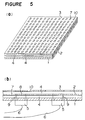
- Figure 5 is a diagram showing a conventional radiowave receiving array antenna wherein reference numeral 1 designates a lower earthing conductor, numeral 2 designates a feeder circuit board, numeral 3 designates an upper earthing conductor, numerals 4 designate supporting plates, numerals 5 designate low noise amplifiers, numerals 6 designate power source lines for the low noise amplifiers, numeral 7 designates a number of radiation elements, numeral 8 designates a feeder circuit, numerals 9 designate a metal pins and numeral 10 designates a number of radiation windows.
- radiowaves received by the radiation elements 7 in the feeder circuit board are synthesized by the feeder circuit 2, the synthesized signal is amplified by the low noise amplifiers 5, and then, is supplied to a receiver.
- the feeder circuit 2 a loss of electric energy produces noises, whereby the quality of an electric signal is deteriorated.
- the a level of deterioration exceeds an allowable range, it is necessary to divide the antenna into sub-arrays and to insert the low noise amplifiers 5 in each sub-array.
- influence by a loss produced in the feeder circuit from the low noise amplifiers 5 to the output terminals of the antenna can be reduced in inverse proportion to the gain of the low noise amplifiers 5 by inserting a plurality of low noise amplifiers 5 in the feeder circuit 2.
- the conventional radiowave receiving array antenna having the construction described above had disadvantages as follows.
- the structure for connecting the low noise amplifiers to the feeder circuit is complicated to thereby increase cost.
- the low noise amplifiers are mounted on the back surface of the lower earthing conductor, the thickness of the antenna device is increased.
- a cover for protecting the low noise amplifiers is additionally needed, whereby the construction is further complicated to thereby increase cost.
- a radiowave receiving array antenna comprising a lower earthing conductive plate, a first supporting plate made of a foamed resinous material which is overlaid on the lower earthing conductive plate, a feeder circuit board comprising a feeder circuit and radiation elements formed on an insulating film which is overlaid on the first supporting plate, a second supporting plate made of a foamed resinous material which is overlaid on the feeder circuit plate, an upper earthing conductive plate made of a metallic substance, overlaid on the second supporting plate, in which radiation windows are formed at positions corresponding to the radiation elements and low noise amplifiers, characterized in that said low noise amplifiers are mounted on spaces formed by thinning out a part of the radiation elements on the feeder circuit board.
- a radiowave receiving array antenna comprising a lower earthing conductive plate, a first supporting plate made of a foamed resinous material which is overlaid on the lower earthing conductive plate, a feeder circuit board comprising a feeder circuit and radiation elements formed on an insulating film which is overlaid on the first supporting plate, a second supporting plate made of a foamed resinous material which is overlaid on the feeder circuit plate, an upper earthing conductive plate made of a metallic substance, overlaid on the second supporting plate, in which radiation windows are formed at positions corresponding to the radiation elements and low noise amplifiers, characterized in that said low noise amplifiers are mounted on microstrip lines at spaces formed by thinning out a part of the radiation elements on the feeder circuit board, and a converting device comprising a rectangular coaxial member is inserted between a microstrip line and a triplate line of the feeder circuit.
- a radiowave receiving array antenna comprising a lower earthing conductive plate, a first supporting plate made of a foamed resinous material which is overlaid on the lower earthing conductive plate, a feeder circuit board comprising a feeder circuit and radiation elements formed on an insulating film which is overlaid on the first supporting plate, a second supporting plate made of a foamed resinous material which is overlaid on the feeder circuit board, an upper earthing conductive plate made of a metallic substance, overlaid on the second supporting plate, in which radiation windows are formed at positions corresponding to the radiation elements and low noise amplifiers, characterized in that said low noise amplifiers are mounted on spaces formed by thinning out a part of the radiation elements on the feeder circuit board, and a power source line for the low noise amplifiers is formed on the upper earthing conductive plate.
- a radiowave receiving array antenna comprising a lower earthing conductive plate, a first supporting plate made of a foamed resinous material which is overlaid on the lower earthing conductive plate, a feeder circuit board comprising a feeder circuit and radiation elements formed on an insulating film which is overlaid on the first supporting plate, a second supporting plate made of a foamed resinous material which is overlaid on the feeder circuit board, an upper earthing conductive plate made of a metallic substance, overlaid on the second supporting plate, in which radiation windows are formed at positions corresponding to the radiation elements and low noise amplifiers, characterized in that said low noise amplifiers are mounted on spaces formed by thinning out a part of the radiation elements on the feeder circuit board; said upper earthing conductive plate is arranged at the lower surface of a double-side-metal-sheet-lined substrate; and a power source line for the low noise amplifiers is formed on said substrate.
- connection of the low noise amplifiers to the feeder circuit can be easy because the low noise amplifiers are mounted on the same plane as the feeder circuit.
- the low noise amplifiers were generally formed on microstrip lines. Insertion of the converting device comprising a rectangular coaxial member between a triplate line and a microstrip line in the feeder circuit assures effective conversion and provides a simple and efficient structure.
- the upper earthing conductor is covered by a radome. Accordingly, the low noise amplifiers can be mounted, without the necessity of an additional protecting means, by arranging the power source lines for the amplifiers on the upper earthing conductor.
- the power source lines for the upper earthing conductor and the low noise amplifiers are formed, by etching or the like, on both surfaces of a double-side-metal-sheet-lined substrate, whereby the number of elements can be reduced so that the manufacturing cost can be reduced.
- reference numeral 1 designates a lower earthing conductor or a lower earthing conductive plate
- numeral 2 designates a feeder circuit board comprising an insulating film on which a feeder circuit is formed
- numeral 3 designates an upper earthing conductor or an upper earthing conductive plate made of a metallic substance
- numerals 4 designate first and second supporting plates made of a foamed resinous material
- numeral 5 designate low noise amplifiers
- numeral 7 designate a number of radiation elements formed on the insulating film which is overlaid on the first supporting plate 4
- numeral 8 designates the feeder circuit
- numeral 10 designate a number of radiation windows formed in the upper earthing conductor 3.
- the feeder circuit board 2 is sandwiched between the first and second supporting plates 4; the upper earthing conductor 3 is overlaid on the other surface of the first supporting plate 4 and the lower earthing conductor 1 is overlaid on the other surface of the second supporting plate 4.
- the low noise amplifiers 5 are mounted on the same plane as the feeder circuit board 2. In comparison with the conventional technique wherein the low noise amplifiers are mounted on the back surface of the lower earthing conductor 1 ( Figure 5), it is unnecessary to provide means for connecting the low noise amplifiers 5 to the feeder circuit 8, on the lower earthing conductor 1. Further, it is unnecessary to provide a cover for protecting the low noise amplifiers 5. In order to mount the low noise amplifiers on the same plane as the feeder circuit board 2, it is necessary to create spaces by sacrificing a part of the radiation elements 7. However, if the number of the radiation elements is sufficiently large, the deterioration of the characteristics of the antenna due to the reduction of the number of the radiation elements is negligible.
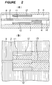
- Figure 2 shows another embodiment of the array antenna according to the present invention.
- the same reference numerals as in Figure 1 designate the same element, and therefore, description of these elements is omitted.
- reference numeral 11 designates a rectangular coaxial type inner conductor
- numeral 12 designates a rectangular coaxial type outer conductor
- numeral 13 designates a microstrip line for a low noise amplifier
- numeral 14 designates an earthing conductor for the microstrip line 16.
- the rectangular coaxial type inner and outer conductors 11, 12 constitutes a converting device.
- the insertion of the converting device between the microstrip line and a triplate line suppresses the deterioration of efficiency of transmitting electromagnetic waves.
- the deterioration of the transmission efficiency is caused because the microstrip line forms an imbalance type transmission path and the triplate line forms a balance type transmission path, and therefore, if the both lines are directly connected, imbalanced, undesired electromagnetic waves are produced at the connection area so as to keep the continuity of electric field, to thereby deteriorate the transmission efficiency.
- the rectangular coaxial type converting device forms a balance type transmission path.
- the converting device comprising rectangular coaxial type inner and outer conductors is inserted in a converting section where there are the microstrip line 13 for a low noise amplifier and the triplate line in the feeder circuit 8, wherein the dimension of the longer inner side of the outer conductor is determined to be able to cut off a waveguide mode at an available frequency.
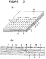
- Figure 3 shows another embodiment of the antenna array according to the present invention.
- the same reference numerals as in Figure 1 designate the same elements except that the array antenna of this embodiment has a radome 15.
- the radome 15 is generally attached to an array antenna for outdoor use. Accordingly, by arranging the power source lines 6 for the low noise amplifiers between the upper earthing conductor 3 and the radome 15, it is unnecessary to provide an additional protecting means for the power source lines 6.
- Figure 4 shows another embodiment of the array antenna according to the present invention.
- the same reference numerals as in Figure 1 designate the same or corresponding elements except that numeral 9 designate metal pins and numeral 16 designates a double-side-metal-sheet-lined substrate.
- the upper earthing conductor 3 and the power source lines 6 are formed, by etching or the like, on both surfaces of a single double-side-metal-sheet-lined substrate, whereby the number of structural elements can be further reduced.
- low noise amplifiers are mounted on the same plane as a feeder circuit, or power source lines are arranged on the upper earthing conductor, whereby the construction of an array antenna can be simplified and the manufacturing cost can be reduced.
Landscapes
- Variable-Direction Aerials And Aerial Arrays (AREA)
- Waveguide Aerials (AREA)
Applications Claiming Priority (2)
| Application Number | Priority Date | Filing Date | Title |
|---|---|---|---|
| JP3056826A JP2725464B2 (ja) | 1991-03-20 | 1991-03-20 | 通信受信用アレーアンテナ |
| JP56826/91 | 1991-03-20 |
Publications (2)
| Publication Number | Publication Date |
|---|---|
| EP0504842A1 true EP0504842A1 (fr) | 1992-09-23 |
| EP0504842B1 EP0504842B1 (fr) | 1996-03-06 |
Family
ID=13038185
Family Applications (1)
| Application Number | Title | Priority Date | Filing Date |
|---|---|---|---|
| EP92104692A Expired - Lifetime EP0504842B1 (fr) | 1991-03-20 | 1992-03-18 | Réseau d'antennes |
Country Status (4)
| Country | Link |
|---|---|
| US (1) | US5218368A (fr) |
| EP (1) | EP0504842B1 (fr) |
| JP (1) | JP2725464B2 (fr) |
| DE (1) | DE69208700T2 (fr) |
Cited By (4)
| Publication number | Priority date | Publication date | Assignee | Title |
|---|---|---|---|---|
| EP0690522A3 (fr) * | 1994-06-28 | 1998-03-11 | Comsat Corporation | Antenne plane avec bloc convertisseur à faible bruit (LNB) à couplage capacitif an réseau d'alimentation |
| RU2117369C1 (ru) * | 1997-07-22 | 1998-08-10 | Товарищество с ограниченной ответственностью "ФАРКОМ" | Фазированная антенная решетка |
| RU2144721C1 (ru) * | 1998-04-24 | 2000-01-20 | Общество с ограниченной ответственностью конструкторское бюро "Пульс" | Плоская антенная решетка с различными поляризациями |
| EP0798807A3 (fr) * | 1996-03-29 | 2000-04-05 | Hitachi, Ltd. | Antenne réseau à fentes du type TEM |
Families Citing this family (7)
| Publication number | Priority date | Publication date | Assignee | Title |
|---|---|---|---|---|
| JP2674345B2 (ja) * | 1991-04-08 | 1997-11-12 | 三菱電機株式会社 | 通信受信用アレーアンテナ |
| US5471220A (en) * | 1994-02-17 | 1995-11-28 | Itt Corporation | Integrated adaptive array antenna |
| US5841401A (en) * | 1996-08-16 | 1998-11-24 | Raytheon Company | Printed circuit antenna |
| JP3471617B2 (ja) * | 1997-09-30 | 2003-12-02 | 三菱電機株式会社 | 平面アンテナ装置 |
| US6262495B1 (en) * | 1998-03-30 | 2001-07-17 | The Regents Of The University Of California | Circuit and method for eliminating surface currents on metals |
| JP3585793B2 (ja) * | 1999-11-09 | 2004-11-04 | 富士通株式会社 | 両面薄膜配線基板の製造方法 |
| US6947003B2 (en) * | 2002-06-06 | 2005-09-20 | Oki Electric Industry Co., Ltd. | Slot array antenna |
Citations (5)
| Publication number | Priority date | Publication date | Assignee | Title |
|---|---|---|---|---|
| EP0055324A2 (fr) * | 1980-11-17 | 1982-07-07 | Ball Corporation | Circuit intégré monolithique à micro-onde avec assemblage d'antenne intégral |
| EP0101791A2 (fr) * | 1982-08-30 | 1984-03-07 | Olin Corporation | Circuit à plusieurs couches |
| EP0346125A2 (fr) * | 1988-06-08 | 1989-12-13 | Nec Corporation | Dispositif microondes intégré pour récepteur de diffusion par satellite |
| US5019829A (en) * | 1989-02-08 | 1991-05-28 | Heckman Douglas E | Plug-in package for microwave integrated circuit having cover-mounted antenna |
| US5023624A (en) * | 1988-10-26 | 1991-06-11 | Harris Corporation | Microwave chip carrier package having cover-mounted antenna element |
Family Cites Families (10)
| Publication number | Priority date | Publication date | Assignee | Title |
|---|---|---|---|---|
| US3757342A (en) * | 1972-06-28 | 1973-09-04 | Cutler Hammer Inc | Sheet array antenna structure |
| JPS6312501A (ja) * | 1986-06-30 | 1988-01-19 | 松下電器産業株式会社 | 厨芥処理機 |
| JPH01158808A (ja) * | 1987-12-15 | 1989-06-21 | Sony Corp | 平面アレイアンテナ |
| JPS6441505A (en) * | 1987-08-07 | 1989-02-13 | Sharp Kk | Plane antenna |
| JPS6479514A (en) * | 1987-09-18 | 1989-03-24 | Yamatake Honeywell Co Ltd | Combustion safety device |
| JPH01103006A (ja) * | 1987-10-15 | 1989-04-20 | Matsushita Electric Works Ltd | 平面アンテナ |
| GB2226919B (en) * | 1988-11-12 | 1993-07-21 | Matsushita Electric Works Ltd | Converter for planar antenna |
| JPH0358602A (ja) * | 1989-07-27 | 1991-03-13 | Hitachi Chem Co Ltd | 平面アンテナ |
| US5083132A (en) * | 1990-04-30 | 1992-01-21 | Matsushita Electric Works, Ltd. | Planar antenna with active circuit block |
| JPH04241502A (ja) * | 1991-01-14 | 1992-08-28 | Sumitomo Electric Ind Ltd | 受信装置 |
-
1991
- 1991-03-20 JP JP3056826A patent/JP2725464B2/ja not_active Expired - Fee Related
-
1992
- 1992-03-18 EP EP92104692A patent/EP0504842B1/fr not_active Expired - Lifetime
- 1992-03-18 DE DE69208700T patent/DE69208700T2/de not_active Expired - Fee Related
- 1992-03-20 US US07/854,252 patent/US5218368A/en not_active Expired - Fee Related
Patent Citations (5)
| Publication number | Priority date | Publication date | Assignee | Title |
|---|---|---|---|---|
| EP0055324A2 (fr) * | 1980-11-17 | 1982-07-07 | Ball Corporation | Circuit intégré monolithique à micro-onde avec assemblage d'antenne intégral |
| EP0101791A2 (fr) * | 1982-08-30 | 1984-03-07 | Olin Corporation | Circuit à plusieurs couches |
| EP0346125A2 (fr) * | 1988-06-08 | 1989-12-13 | Nec Corporation | Dispositif microondes intégré pour récepteur de diffusion par satellite |
| US5023624A (en) * | 1988-10-26 | 1991-06-11 | Harris Corporation | Microwave chip carrier package having cover-mounted antenna element |
| US5019829A (en) * | 1989-02-08 | 1991-05-28 | Heckman Douglas E | Plug-in package for microwave integrated circuit having cover-mounted antenna |
Non-Patent Citations (3)
| Title |
|---|
| PATENT ABSTRACTS OF JAPAN vol. 13, no. 354 (E-802)(3702), 8 August 1989; & JP - A - 1114104 (MATSUSHITA ELECTRIC) 02.05.1989 * |
| PATENT ABSTRACTS OF JAPAN vol. 13, no. 354 (E-802)(3702), 8 August 1989; & JP - A - 1114105 (MATSUSHITA ELECTRIC) 02.05.1989 * |
| PATENT ABSTRACTS OF JAPAN vol. 13, no. 354 (E-802)(3702), 8 August 1989; & JP - A - 1114106 (MATSUSHITA ELECTRIC) 02.05.1989 * |
Cited By (4)
| Publication number | Priority date | Publication date | Assignee | Title |
|---|---|---|---|---|
| EP0690522A3 (fr) * | 1994-06-28 | 1998-03-11 | Comsat Corporation | Antenne plane avec bloc convertisseur à faible bruit (LNB) à couplage capacitif an réseau d'alimentation |
| EP0798807A3 (fr) * | 1996-03-29 | 2000-04-05 | Hitachi, Ltd. | Antenne réseau à fentes du type TEM |
| RU2117369C1 (ru) * | 1997-07-22 | 1998-08-10 | Товарищество с ограниченной ответственностью "ФАРКОМ" | Фазированная антенная решетка |
| RU2144721C1 (ru) * | 1998-04-24 | 2000-01-20 | Общество с ограниченной ответственностью конструкторское бюро "Пульс" | Плоская антенная решетка с различными поляризациями |
Also Published As
| Publication number | Publication date |
|---|---|
| JPH04291807A (ja) | 1992-10-15 |
| JP2725464B2 (ja) | 1998-03-11 |
| US5218368A (en) | 1993-06-08 |
| EP0504842B1 (fr) | 1996-03-06 |
| DE69208700T2 (de) | 1996-10-31 |
| DE69208700D1 (de) | 1996-04-11 |
Similar Documents
| Publication | Publication Date | Title |
|---|---|---|
| USH956H (en) | Waveguide fed spiral antenna | |
| EP0253128B1 (fr) | Antenne à micro-ondes | |
| US5825333A (en) | Offset multibeam antenna | |
| US5892482A (en) | Antenna mutual coupling neutralizer | |
| US4829314A (en) | Microwave plane antenna simultaneously receiving two polarizations | |
| EP0203777B1 (fr) | Amplificateur spatial | |
| JP2022504700A (ja) | 非接触式マイクロストリップ-導波路変換器 | |
| EP0504842B1 (fr) | Réseau d'antennes | |
| US6661386B1 (en) | Through glass RF coupler system | |
| WO2001041257A1 (fr) | Dispositif d'antenne a circuit emetteur-recepteur | |
| US4641106A (en) | Radial power amplifier | |
| EP0135508B1 (fr) | Coupleur coaxial a conducteur carre | |
| EP0110324B1 (fr) | Récepteur à hyperfréquences comportant un filtre à guide d'ondes | |
| US7199758B2 (en) | Antenna device | |
| JPH05259713A (ja) | 同軸マイクロストリップ線路変換器 | |
| JPH0340961B2 (fr) | ||
| US5194875A (en) | Notch radiator elements | |
| US6239766B1 (en) | Radiation shielding device | |
| US5914684A (en) | Electromagnetic transducer system with integrated circuit card adapter | |
| US4652839A (en) | Waveguide-to-coaxial converter | |
| US3806945A (en) | Stripline antenna | |
| EP0500949B1 (fr) | Circuit hyperfrequence | |
| JP2613170B2 (ja) | 広帯域平面アンテナ | |
| JPS592402A (ja) | 導波管−マイクロストリツプ線路変換器 | |
| JP3387018B2 (ja) | 直交2偏波導波管入力装置および当該直交2偏波導波管入力装置を用いた衛星放送受信用のコンバータ |
Legal Events
| Date | Code | Title | Description |
|---|---|---|---|
| PUAI | Public reference made under article 153(3) epc to a published international application that has entered the european phase |
Free format text: ORIGINAL CODE: 0009012 |
|
| AK | Designated contracting states |
Kind code of ref document: A1 Designated state(s): DE FR GB |
|
| 17P | Request for examination filed |
Effective date: 19930114 |
|
| 17Q | First examination report despatched |
Effective date: 19941216 |
|
| GRAA | (expected) grant |
Free format text: ORIGINAL CODE: 0009210 |
|
| AK | Designated contracting states |
Kind code of ref document: B1 Designated state(s): DE FR GB |
|
| REF | Corresponds to: |
Ref document number: 69208700 Country of ref document: DE Date of ref document: 19960411 |
|
| ET | Fr: translation filed | ||
| PLBE | No opposition filed within time limit |
Free format text: ORIGINAL CODE: 0009261 |
|
| STAA | Information on the status of an ep patent application or granted ep patent |
Free format text: STATUS: NO OPPOSITION FILED WITHIN TIME LIMIT |
|
| 26N | No opposition filed | ||
| PGFP | Annual fee paid to national office [announced via postgrant information from national office to epo] |
Ref country code: FR Payment date: 19990309 Year of fee payment: 8 |
|
| PGFP | Annual fee paid to national office [announced via postgrant information from national office to epo] |
Ref country code: GB Payment date: 19990318 Year of fee payment: 8 |
|
| PGFP | Annual fee paid to national office [announced via postgrant information from national office to epo] |
Ref country code: DE Payment date: 19990326 Year of fee payment: 8 |
|
| PG25 | Lapsed in a contracting state [announced via postgrant information from national office to epo] |
Ref country code: GB Free format text: LAPSE BECAUSE OF NON-PAYMENT OF DUE FEES Effective date: 20000318 |
|
| GBPC | Gb: european patent ceased through non-payment of renewal fee |
Effective date: 20000318 |
|
| PG25 | Lapsed in a contracting state [announced via postgrant information from national office to epo] |
Ref country code: FR Free format text: LAPSE BECAUSE OF NON-PAYMENT OF DUE FEES Effective date: 20001130 |
|
| REG | Reference to a national code |
Ref country code: FR Ref legal event code: ST |
|
| PG25 | Lapsed in a contracting state [announced via postgrant information from national office to epo] |
Ref country code: DE Free format text: LAPSE BECAUSE OF NON-PAYMENT OF DUE FEES Effective date: 20010103 |