EP0508734B1 - Filtre céramique - Google Patents
Filtre céramique Download PDFInfo
- Publication number
- EP0508734B1 EP0508734B1 EP19920303092 EP92303092A EP0508734B1 EP 0508734 B1 EP0508734 B1 EP 0508734B1 EP 19920303092 EP19920303092 EP 19920303092 EP 92303092 A EP92303092 A EP 92303092A EP 0508734 B1 EP0508734 B1 EP 0508734B1
- Authority
- EP
- European Patent Office
- Prior art keywords
- resonators
- filter
- coupling
- filter according
- resonator
- Prior art date
- Legal status (The legal status is an assumption and is not a legal conclusion. Google has not performed a legal analysis and makes no representation as to the accuracy of the status listed.)
- Expired - Lifetime
Links
- 239000000919 ceramic Substances 0.000 title description 23
- 230000008878 coupling Effects 0.000 claims description 29
- 238000010168 coupling process Methods 0.000 claims description 29
- 238000005859 coupling reaction Methods 0.000 claims description 29
- 230000005540 biological transmission Effects 0.000 claims description 17
- 230000001939 inductive effect Effects 0.000 claims description 9
- 238000002955 isolation Methods 0.000 claims description 7
- 239000003989 dielectric material Substances 0.000 claims description 3
- 239000004020 conductor Substances 0.000 description 9
- 238000005192 partition Methods 0.000 description 8
- 238000000576 coating method Methods 0.000 description 5
- 239000003990 capacitor Substances 0.000 description 4
- 239000011248 coating agent Substances 0.000 description 4
- 230000012447 hatching Effects 0.000 description 3
- 238000005476 soldering Methods 0.000 description 3
- 230000000694 effects Effects 0.000 description 2
- 238000004519 manufacturing process Methods 0.000 description 2
- 239000000463 material Substances 0.000 description 2
- 238000004904 shortening Methods 0.000 description 2
- 239000005749 Copper compound Substances 0.000 description 1
- RTAQQCXQSZGOHL-UHFFFAOYSA-N Titanium Chemical compound [Ti] RTAQQCXQSZGOHL-UHFFFAOYSA-N 0.000 description 1
- NEIHULKJZQTQKJ-UHFFFAOYSA-N [Cu].[Ag] Chemical compound [Cu].[Ag] NEIHULKJZQTQKJ-UHFFFAOYSA-N 0.000 description 1
- 238000013459 approach Methods 0.000 description 1
- 229910010293 ceramic material Inorganic materials 0.000 description 1
- 238000005520 cutting process Methods 0.000 description 1
- 238000011161 development Methods 0.000 description 1
- 230000018109 developmental process Effects 0.000 description 1
- 238000005516 engineering process Methods 0.000 description 1
- 238000005304 joining Methods 0.000 description 1
- 238000000034 method Methods 0.000 description 1
- 238000012986 modification Methods 0.000 description 1
- 230000004048 modification Effects 0.000 description 1
- 238000012545 processing Methods 0.000 description 1
- 238000000926 separation method Methods 0.000 description 1
Images

Classifications
-
- H—ELECTRICITY
- H01—ELECTRIC ELEMENTS
- H01P—WAVEGUIDES; RESONATORS, LINES, OR OTHER DEVICES OF THE WAVEGUIDE TYPE
- H01P1/00—Auxiliary devices
- H01P1/20—Frequency-selective devices, e.g. filters
- H01P1/213—Frequency-selective devices, e.g. filters combining or separating two or more different frequencies
- H01P1/2136—Frequency-selective devices, e.g. filters combining or separating two or more different frequencies using comb or interdigital filters; using cascaded coaxial cavities
-
- H—ELECTRICITY
- H01—ELECTRIC ELEMENTS
- H01P—WAVEGUIDES; RESONATORS, LINES, OR OTHER DEVICES OF THE WAVEGUIDE TYPE
- H01P1/00—Auxiliary devices
- H01P1/20—Frequency-selective devices, e.g. filters
- H01P1/201—Filters for transverse electromagnetic waves
- H01P1/205—Comb or interdigital filters; Cascaded coaxial cavities
- H01P1/2056—Comb filters or interdigital filters with metallised resonator holes in a dielectric block
Definitions
- This invention relates to ceramic filters comprising two or more transmission line resonators of the coaxial type.
- a ceramic resonator comprises a basic structure, in which a hole is made in a ceramic block of a material with a high dielectric constant, e.g. titanate, the block having side surfaces, a top surface and a bottom surface, and the hole extending from the top surface to the bottom surface.
- the surfaces of the block are coated, except for the top surface, with an electrically conducting material.
- Circuit patterns are applied to the top surface, the circuits capacitively coupling a signal to the resonator and outputting the signal.
- the structure forms a transmission line resonator whose resonant frequency is determined by the length of the hole, i.e. by the thickness of the block.
- the length of the hole is dimensioned so that a transmission line resonator of a quarter-wave length is obtained.
- Band-stop filters using ceramic technology became commercially available only recently. It is characteristic to all these known band-stop filters, that the filter is composed of separate resonators and a desired number of these coated separate resonator blocks are arranged in a row, whereby a band-stop filter is obtained with a desired bandwidth and center frequency.
- each resonator block forms a draining circuit, and these draining circuits are then coupled in a series through inductive or reactive circuits, connecting the upper ends of the resonators using e.g. a separate transmission line length.
- the isolation between the separate resonators is formed with the same coating, which forms an effective partition between the blocks.
- Duplex filters are commonly used in radio transceivers which have a common antenna. Such filters comprise two individual band-pass filters, one being connected in the receiving branch and having a center frequency and a bandwidth corresponding to the receiving band, the other filter being connected in the transmission branch and having a center frequency and a bandwidth corresponding to the transmission band. Often the other ends of the filters are connected through a transmission line to the common antenna line. While the duplex filter often is located in a common housing with interfaces for the transmitter, the receiver and the antenna, in practice however it will be formed by two individual band-pass filters, because a very high isolation between the filters must be obtained so that their mutual electromagnetic leaks do not interfere with the operation.
- These filters are made so that first the transmission branch band-pass filter and the receiving branch band-pass filter are made separately, each thus having interfaces for the antenna and for the receiver/transmitter.
- the ceramic bodies of both filters are coated with a conductive layer on the side surfaces and on the bottom surface.
- the finished filters are soldered onto a common support, that may be a board, a frame, or the like. At the same time the ceramic bodies are mutually fixed by soldering at the end faces. Soldering is possible, because the outer surfaces of the ceramic bodies are coated.
- the antenna interfaces are joined into one interface, and so a duplex filter is obtained, virtually comprising a single block.
- a disadvantage of all these filters assembled of separate blocks is that a filter made of many blocks requires a high production capacity, because every block is separately sintered and coated, and the blocks are electrically individually connected to each other, usually by soldering the connecting wires by hand. Further the separate blocks must be fastened to some mounting support in a mechanically reliable way. The electrical and mechanical connection of the blocks is a cumbersome and slow operation. In other words, the production capacity must be doubled compared to a situation where it would be possible to make the whole filter in a single ceramic block.
- US patent 4,823,098, Motorola describes a monolithic ceramic filter with band-stop characteristics.
- the filter comprises seven resonators located in the same ceramic block, of which three operate as a band-stop filter and the other as a band-pass filter.
- the resonators in the band-stop section are interconnected via quarter-wave transmission lines.
- the transmission lines invert the impedance of the resonators, so that the resonators generate zeros in the filter. It is stated in the publication, that by sawing it is possible to separate said three filters from the block and to coat the new side wall obtained in the cutting with conducting material, whereby the obtained filter operates as an independent band-stop filter with several zeros. It is not mentioned in the publication what influence the inductive coupling between the resonators, effected through the ceramics, has on the filter characteristic, but it seems probable that mutual coupling between the resonators makes it difficult to control the characteristics.
- a filter comprising a body of dielectric material having at least two holes extending from a top to a bottom surface of the body; a conductive layer covering the major portion of the body and the interiors of the holes, except for one of the side faces of the body which is substantially uncoated so as to form at least two transmission line resonators; and an electrically conductive electrode pattern provided on the uncoated side of the body for providing electrical signal coupling to and from the resonators characterized in that at least one conductive region is provided on the uncoated side, the region extending between the top and bottom surfaces of the body between two of the at least two resonators and whereby the two resonators separated by said region are substantially electrically and magnetically isolated from each other.
- the invention is based on the development of the resonator circuits described in the above mentioned European patent application.
- a conducting area i.e., a coating on the surface of the uncoated side between the resonator circuits of a ceramic filter block
- the electric and magnetic coupling between the resonators can be adjusted close to zero.
- this conducting area is made in the form of a strip extending from the ceramic block bottom surface, where it is in contact with the conducting coating of the block, up to the upper surface of the side, an almost perfect electric and magnetic isolation is obtained between the resonators.
- the conducting areas according to the invention provide in a sense an electric "partition" between the resonators.
- a band-stop filter 1 according to a first embodiment the invention comprises three transmission line resonators A, B and C.
- a bar-like block of ceramic material is provided with holes 21, 22 and 23 extending from the top surface 3 to the bottom surface of the block.
- the holes, the bottom surface, the ends, and one side of the block are coated with conducting material, e.g. with a silver-copper compound.
- the top surface 3 can also be coated, except for a narrow annular area around the upper edge of the holes 21, 22 and 23.
- a circuit pattern 5 is applied with the aid of a mask on the uncoated side 4 of the block, the pattern including a strip around the edge of the uncoated side 4.
- Contact points 9, 10 and 11 are also applied using the mask to the side 4 of each resonator.
- Conducting areas 14 and 15, located between the resonators, are made with the same mask, the areas extending from the block bottom edge, where they join the strip extending along the bottom edge of the side 4, to the top edge of the block, where they join the strip extending along the top edge of the side 4.
- the circuit pattern formed with the mask is shown by hatching.
- the end surface of the block, being one of the coated surfaces, is also shown by hatching.
- To the circuit pattern are connected the required components and wires for the coupling of signals to the filter, for interconnection of the resonators, and for outputting the signal from the filter.
- the high frequency signal is input with wire IN to the connection point 9 at the middle of resonator A.
- a block capacitor 6 is connected between this point 9 and the conducting strip at the bottom edge of the side 4.
- the signal is coupled from resonator A via the connecting wire 12 to the connection point 10 of second resonator B, which is also connected to the strip at the bottom edge of the uncoated side 4 of the side through a block capacitor 7.
- the connecting wire 12 represents a defined inductance.
- the resonator B is connected to the resonator C with a wire 13 representing an inductance, and the connection point 11 is connected to the strip at the bottom edge of the uncoated side 4 through a block capacitor 8.
- the signal is then outputted from the point 11 and out from the filter 1 along the conductor OUT.
- the side of the block is covered with a metallic protecting cover, so that a small gap is left between the cover and the side surface.
- the coupling between the resonators can be increased in that the conducting area between the resonators is shortened, as in the area 14 between the resonators A and B, or the conducting area is narrowed, as is made in the area 15 between the resonators B and C. It is also possible to use a combination of these.
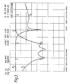
- Figure 3 shows the actual measured attenuation curve for a band-stop filter manufactured according to the invention in a single ceramic block.
- the realized filter is particularly intended to attenuate the frequency band 890 - 915 MHz, which is the transmission bandwidth of the European digital mobile phone system known as GSM, the filter being suited e.g. for use in the receiving branch in connection with the antenna filter.
- the curve I being an attenuation curve, shows that the attenuation is high, more than 40 dB between the markers 1 and 2 constituting said frequency band, and thereafter the attenuation rapidly approaches zero. This is advantageous in that the transmitter frequency will not reach the receiver.
- the curve II shows the matching of the filter.
- a duplex filter 100 is based on a single monolithic ceramic block 103 with parallel holes R1, R2, R3, R4 and T1, T2, T3 extending from the top surface 102 to the bottom surface. All surfaces of the block, except the top surface 102 and the side 105 shown in Figure 4, are entirely coated with an electrically conductive material 104. The internal walls of the holes R1-R4;T1-T3 are also coated, these coatings joining the coating on the bottom. Thus in a known way seven transmission line resonators are formed. The interface to the resonators is accomplished by providing circuit patterns on the uncoated side 105 using a mask, the circuit patterns being formed by conductive areas having a defined shape.
- circuit patterns form for example the conductive areas illustrated in the Figure 4 by hatching, the areas having conductive strips 107 at the top of uncoated side 105 and conductive strips 106 at the bottom of uncoated side 105.
- the pattern includes contact points, 111,113,115,117 where connections are made for the signal wire ANT to the antenna, for the conductor Rx to the receiver and for the conductor Tx to the transmitter.
- block components can also be used; for example the antenna contact point 113 may be connected not only to the transmission line, but also through the block capacitor 108 to the conductive strip 106 at the bottom edge of side 105.
- These circuit patterns are only intended to illustrate the use of circuit patterns on the uncoated side 105 of the ceramic block. Their number, size, and characteristics, and the possible discrete components, will vary according to the characteristics which are desired for the filter.
- the duplex filter is manufactured using a mask in accordance with the method described in more detail in the above mentioned European Patent Application, as is the coupling between the resonators and thus it is not necessary to describe in further detail the provision of the patterns with the aid of a mask.
- a conductive strip 109 extends from the conductive strip 106 at the lower edge of the side 105 to the conductive strip 107 at the upper edge of the side 105, and which is located exactly between the resonators R4 and T1. As described above, this strip 109 causes the capacitive and the inductive coupling to cancel each other out, in other words the coupling between the resonators will be almost zero. In a sense an "electric partition" is formed between the resonators. Due to this two separate filters are formed in the same monolithic ceramic block: the filter D comprising the resonators R1, R2, R3, R4, and the filter E, comprising the resonators T1, T2, T3.
- Filter D is the band-pass filter of the receiver branch
- filter E is the band-pass filter of the transmitter branch. While these filters are on the same ceramic block, they do not interfere with each others operation, because the electric partition provides an almost complete isolation between them.
- the only connection between them is the jumper connection 110 between points 113 and 115 that connects the transmitter branch filter to the antenna interface.
- the side 105 containing the circuit patterns and the interfaces is covered with a conductive cover, whereby the ceramic block is substantially entirely enclosed by a conductive layer.
- the conductive area providing the electrical partition is a continuous strip extending from the lower surface of the side to the upper surface, the width of which has an influence of the separation provided by the electric partition, and thus it is possible to obtain a desired value of coupling between the resonators by varying its width.
- the conductive strip could have an interruption, a non-conductive area of a defined length as described in connection with the first embodiment. This interruption is preferably closer to the lower edge of the side 105, where the inductive coupling is at its highest.
- the interruption enables the realization of the strip 109 as a strip line directly on the wall surface. This interruption also has an effect on the coupling between adjacent resonators R4 and T1 of the filters D and E.
Landscapes
- Physics & Mathematics (AREA)
- Electromagnetism (AREA)
- Control Of Motors That Do Not Use Commutators (AREA)
Claims (10)
- Filtre (1, 100) comprenant
un corps de matériau diélectrique ayant au moins deux trous (2, R, T) s'étendant d'une surface supérieure (3, 102) jusqu'à une surface inférieure du corps ;
une couche conductrice (104) recouvrant la partie principale du corps et les intérieurs de trous, sauf pour une des faces latérales (4, 105) du corps qui est pratiquement non revêtu, de façon à former au moins deux résonateurs de ligne de transmission ; et
un motif d'électrode électriquement conducteur placé sur le côté non revêtu du corps pour assurer le couplage du signal électrique vers les résonateurs et depuis les résonateurs.
caractérisé en ce qu'au moins une région conductrice (14, 15, 109) est prévue sur le côté non revêtu, la région se trouvant entre les surfaces supérieure et inférieure du corps entre deux des au moins deux résonateurs de sorte que les deux résonateurs séparés par lesdites régions sont isolés pratiquement électriquement et magnétiquement l'un de l'autre. - Filtre selon la revendication 1, dans lequel le côté non revêtu est muni de bandes conductrices (5, 106, 107) à ses bords adjacents aux surfaces supérieure et inférieure, les régions conductrices étant connectées à chacune de ses extrémités aux dites bandes.
- Filtre selon la revendication 1 ou la revendication 2, dans lequel la région conductrice présente une discontinuité dans celle-ci afin de procurer un certain couplage magnétique et électrique entre les deux résonateurs.
- Filtre selon la revendication 1 ou la revendication 2, dans lequel la région conductrice présente une certaine largeur de sorte qu'un certain couplage magnétique et électrique entre les deux résonateurs est assuré.
- Filtre selon la revendication 1 ou la revendication 2, dans lequel la région conductrice présente une certaine dimension et forme de sorte que le couplage magnétique et électrique entre les résonateurs est pratiquement nul.
- Filtre selon l'une quelconque des revendications précédentes, incluant un couvercle extérieur métallique.
- Filtre selon l'une quelconque des revendications précédentes, dans lequel le filtre est un filtre coupe-bande (1) comprenant au moins deux résonateurs (A, B, C) dans lequel la région conductrice est prévue entre chaque trous.
- Filtre selon la revendication 7, dans lequel le couplage inductif est assuré entre chaque résonateur par des moyens de couplage (12, 13) pontant lesdites régions conductrices.
- Filtre selon la revendication 7 ou la revendication 8, dans lequel le couplage capacitif (6, 7, 8) est assuré entre chaque résonateur et la bande de conduction inférieure.
- Filtre selon l'une quelconque des revendications 1 à 6, dans lequel le filtre est un filtre duplex (100) comprenant au moins un résonateur (R) formant une première branche (D) du filtre duplex et au moins un résonateur (T) formant une seconde branche (E) du filtre duplex, ladite région conductrice étant placée entre lesdites première et seconde branches afin d'assurer un isolement presque total électrique et magnétique entre celles-ci.
Applications Claiming Priority (4)
| Application Number | Priority Date | Filing Date | Title |
|---|---|---|---|
| FI911797A FI87853C (fi) | 1991-04-12 | 1991-04-12 | Keramiskt spaerrfilter |
| FI911797 | 1991-04-12 | ||
| FI911796 | 1991-04-12 | ||
| FI911796A FI86673C (fi) | 1991-04-12 | 1991-04-12 | Keramiskt duplexfilter. |
Publications (2)
| Publication Number | Publication Date |
|---|---|
| EP0508734A1 EP0508734A1 (fr) | 1992-10-14 |
| EP0508734B1 true EP0508734B1 (fr) | 1995-12-13 |
Family
ID=26158937
Family Applications (1)
| Application Number | Title | Priority Date | Filing Date |
|---|---|---|---|
| EP19920303092 Expired - Lifetime EP0508734B1 (fr) | 1991-04-12 | 1992-04-08 | Filtre céramique |
Country Status (7)
| Country | Link |
|---|---|
| EP (1) | EP0508734B1 (fr) |
| JP (1) | JPH05102705A (fr) |
| AU (1) | AU1398292A (fr) |
| CA (1) | CA2065207A1 (fr) |
| DE (1) | DE69206661T2 (fr) |
| DK (1) | DK0508734T3 (fr) |
| FI (1) | FI87853C (fr) |
Families Citing this family (3)
| Publication number | Priority date | Publication date | Assignee | Title |
|---|---|---|---|---|
| US6008707A (en) * | 1993-11-18 | 1999-12-28 | Murata Manufacturing Co., Ltd. | Antenna duplexer |
| JP3230353B2 (ja) * | 1993-11-18 | 2001-11-19 | 株式会社村田製作所 | アンテナ共用器 |
| DE19903855B4 (de) | 1999-02-01 | 2010-04-15 | Epcos Ag | Antennenweiche |
Family Cites Families (4)
| Publication number | Priority date | Publication date | Assignee | Title |
|---|---|---|---|---|
| JPS6152003A (ja) * | 1984-08-21 | 1986-03-14 | Murata Mfg Co Ltd | 誘電体フイルタ |
| JPH0713284Y2 (ja) * | 1987-09-21 | 1995-03-29 | 株式会社村田製作所 | 一体成形型誘電体フィルタの共振周波数調整構造 |
| JPH01103001A (ja) * | 1987-10-15 | 1989-04-20 | Murata Mfg Co Ltd | 誘電体フィルタ |
| US5103197A (en) * | 1989-06-09 | 1992-04-07 | Lk-Products Oy | Ceramic band-pass filter |
-
1991
- 1991-04-12 FI FI911797A patent/FI87853C/fi not_active IP Right Cessation
-
1992
- 1992-04-02 AU AU13982/92A patent/AU1398292A/en not_active Abandoned
- 1992-04-06 CA CA002065207A patent/CA2065207A1/fr not_active Abandoned
- 1992-04-08 DK DK92303092T patent/DK0508734T3/da active
- 1992-04-08 DE DE1992606661 patent/DE69206661T2/de not_active Expired - Fee Related
- 1992-04-08 EP EP19920303092 patent/EP0508734B1/fr not_active Expired - Lifetime
- 1992-04-10 JP JP4090888A patent/JPH05102705A/ja active Pending
Also Published As
| Publication number | Publication date |
|---|---|
| CA2065207A1 (fr) | 1992-10-13 |
| FI87853C (fi) | 1993-02-25 |
| FI911797A0 (fi) | 1991-04-12 |
| JPH05102705A (ja) | 1993-04-23 |
| EP0508734A1 (fr) | 1992-10-14 |
| AU1398292A (en) | 1992-10-15 |
| DK0508734T3 (da) | 1996-01-22 |
| DE69206661T2 (de) | 1996-05-30 |
| DE69206661D1 (de) | 1996-01-25 |
| FI87853B (fi) | 1992-11-13 |
Similar Documents
| Publication | Publication Date | Title |
|---|---|---|
| US5307036A (en) | Ceramic band-stop filter | |
| US5239279A (en) | Ceramic duplex filter | |
| US4879533A (en) | Surface mount filter with integral transmission line connection | |
| US5103197A (en) | Ceramic band-pass filter | |
| KR0142171B1 (ko) | 세라믹 필터 | |
| US5926079A (en) | Ceramic waveguide filter with extracted pole | |
| US6222431B1 (en) | Balanced dielectric filter | |
| US5812036A (en) | Dielectric filter having intrinsic inter-resonator coupling | |
| CA2116488A1 (fr) | Filtre | |
| CA2089547A1 (fr) | Filtre a bloc dielectrique dote d'inducteurs a ligne de transmission blindee | |
| US5379011A (en) | Surface mount ceramic filter duplexer having reduced input/output coupling and adjustable high-side transmission zeroes | |
| EP1592080A2 (fr) | Dispositif diélectrique | |
| EP0899806B1 (fr) | Filtre diélectrique, duplexeur et système de communication | |
| EP0508734B1 (fr) | Filtre céramique | |
| JPH0234001A (ja) | 帯域阻止フイルタ | |
| KR100305577B1 (ko) | 유전체 듀플렉서의 제조방법 | |
| JP3349345B2 (ja) | 面実装型誘電体フィルタ | |
| KR100332879B1 (ko) | 유전체 듀플렉서 및 그 제조방법 | |
| JPH07283611A (ja) | 誘電体共振器装置 | |
| JP2003298309A (ja) | 積層型誘電体フィルタ | |
| JPH01223802A (ja) | 誘電体フィルタ | |
| JPH0758520A (ja) | 誘電体分波器 |
Legal Events
| Date | Code | Title | Description |
|---|---|---|---|
| PUAI | Public reference made under article 153(3) epc to a published international application that has entered the european phase |
Free format text: ORIGINAL CODE: 0009012 |
|
| AK | Designated contracting states |
Kind code of ref document: A1 Designated state(s): CH DE DK FR GB IT LI SE |
|
| 17P | Request for examination filed |
Effective date: 19921127 |
|
| 17Q | First examination report despatched |
Effective date: 19940811 |
|
| GRAA | (expected) grant |
Free format text: ORIGINAL CODE: 0009210 |
|
| AK | Designated contracting states |
Kind code of ref document: B1 Designated state(s): CH DE DK FR GB IT LI SE |
|
| REG | Reference to a national code |
Ref country code: DK Ref legal event code: T3 |
|
| REF | Corresponds to: |
Ref document number: 69206661 Country of ref document: DE Date of ref document: 19960125 |
|
| ET | Fr: translation filed | ||
| REG | Reference to a national code |
Ref country code: CH Ref legal event code: NV Representative=s name: E. BLUM & CO. PATENTANWAELTE |
|
| ITF | It: translation for a ep patent filed | ||
| PLBE | No opposition filed within time limit |
Free format text: ORIGINAL CODE: 0009261 |
|
| STAA | Information on the status of an ep patent application or granted ep patent |
Free format text: STATUS: NO OPPOSITION FILED WITHIN TIME LIMIT |
|
| 26N | No opposition filed | ||
| PGFP | Annual fee paid to national office [announced via postgrant information from national office to epo] |
Ref country code: GB Payment date: 19970401 Year of fee payment: 6 |
|
| PGFP | Annual fee paid to national office [announced via postgrant information from national office to epo] |
Ref country code: FR Payment date: 19970409 Year of fee payment: 6 |
|
| PGFP | Annual fee paid to national office [announced via postgrant information from national office to epo] |
Ref country code: DK Payment date: 19970414 Year of fee payment: 6 Ref country code: DE Payment date: 19970414 Year of fee payment: 6 |
|
| PGFP | Annual fee paid to national office [announced via postgrant information from national office to epo] |
Ref country code: SE Payment date: 19970418 Year of fee payment: 6 |
|
| PGFP | Annual fee paid to national office [announced via postgrant information from national office to epo] |
Ref country code: CH Payment date: 19970422 Year of fee payment: 6 |
|
| PG25 | Lapsed in a contracting state [announced via postgrant information from national office to epo] |
Ref country code: GB Free format text: LAPSE BECAUSE OF NON-PAYMENT OF DUE FEES Effective date: 19980408 |
|
| PG25 | Lapsed in a contracting state [announced via postgrant information from national office to epo] |
Ref country code: SE Free format text: LAPSE BECAUSE OF NON-PAYMENT OF DUE FEES Effective date: 19980409 |
|
| PG25 | Lapsed in a contracting state [announced via postgrant information from national office to epo] |
Ref country code: LI Free format text: LAPSE BECAUSE OF NON-PAYMENT OF DUE FEES Effective date: 19980430 Ref country code: FR Free format text: THE PATENT HAS BEEN ANNULLED BY A DECISION OF A NATIONAL AUTHORITY Effective date: 19980430 Ref country code: DK Free format text: LAPSE BECAUSE OF NON-PAYMENT OF DUE FEES Effective date: 19980430 Ref country code: CH Free format text: LAPSE BECAUSE OF NON-PAYMENT OF DUE FEES Effective date: 19980430 |
|
| GBPC | Gb: european patent ceased through non-payment of renewal fee |
Effective date: 19980408 |
|
| REG | Reference to a national code |
Ref country code: CH Ref legal event code: PL |
|
| EUG | Se: european patent has lapsed |
Ref document number: 92303092.8 |
|
| PG25 | Lapsed in a contracting state [announced via postgrant information from national office to epo] |
Ref country code: DE Free format text: LAPSE BECAUSE OF NON-PAYMENT OF DUE FEES Effective date: 19990202 |
|
| REG | Reference to a national code |
Ref country code: FR Ref legal event code: ST |
|
| REG | Reference to a national code |
Ref country code: DK Ref legal event code: EBP |
|
| PG25 | Lapsed in a contracting state [announced via postgrant information from national office to epo] |
Ref country code: IT Free format text: LAPSE BECAUSE OF NON-PAYMENT OF DUE FEES Effective date: 20050408 |