EP0512463A1 - Verfahren zur Herstellung von dynamischer Speichern mit wahlfreiem Zugriff - Google Patents
Verfahren zur Herstellung von dynamischer Speichern mit wahlfreiem Zugriff Download PDFInfo
- Publication number
- EP0512463A1 EP0512463A1 EP92107517A EP92107517A EP0512463A1 EP 0512463 A1 EP0512463 A1 EP 0512463A1 EP 92107517 A EP92107517 A EP 92107517A EP 92107517 A EP92107517 A EP 92107517A EP 0512463 A1 EP0512463 A1 EP 0512463A1
- Authority
- EP
- European Patent Office
- Prior art keywords
- layer
- dielectric material
- array
- bitline
- deposition
- Prior art date
- Legal status (The legal status is an assumption and is not a legal conclusion. Google has not performed a legal analysis and makes no representation as to the accuracy of the status listed.)
- Withdrawn
Links
Images






Classifications
-
- H—ELECTRICITY
- H10—SEMICONDUCTOR DEVICES; ELECTRIC SOLID-STATE DEVICES NOT OTHERWISE PROVIDED FOR
- H10B—ELECTRONIC MEMORY DEVICES
- H10B12/00—Dynamic random access memory [DRAM] devices
- H10B12/01—Manufacture or treatment
- H10B12/02—Manufacture or treatment for one transistor one-capacitor [1T-1C] memory cells
- H10B12/03—Making the capacitor or connections thereto
- H10B12/033—Making the capacitor or connections thereto the capacitor extending over the transistor
-
- H—ELECTRICITY
- H10—SEMICONDUCTOR DEVICES; ELECTRIC SOLID-STATE DEVICES NOT OTHERWISE PROVIDED FOR
- H10W—GENERIC PACKAGES, INTERCONNECTIONS, CONNECTORS OR OTHER CONSTRUCTIONAL DETAILS OF DEVICES COVERED BY CLASS H10
- H10W20/00—Interconnections in chips, wafers or substrates
- H10W20/40—Interconnections external to wafers or substrates, e.g. back-end-of-line [BEOL] metallisations or vias connecting to gate electrodes
- H10W20/41—Interconnections external to wafers or substrates, e.g. back-end-of-line [BEOL] metallisations or vias connecting to gate electrodes characterised by their conductive parts
- H10W20/44—Conductive materials thereof
- H10W20/4451—Semiconductor materials, e.g. polysilicon
Definitions
- This invention relates to semiconductor manufacturing technology and, more specifically, to techniques for minimizing the spacing between word lines required to create buried contacts in dynamic random access memories of stacked-cell design.
- the memory cells of dynamic random access memories are comprised of two main components: a field-effect transistor and a capacitor.
- a field-effect transistor In DRAM cells utilizing a conventional planar capacitor, far more chip surface area is dedicated to the planar capacitor than to the field-effect transistor (FET).
- Wordlines are generally etched from a polysilicon-1 layer.
- a doped region of silicon substrate functions as the lower (storage-node) capacitor plate, while a polysilicon-2 generally functions as the upper capacitor plate (cell plate).
- planar capacitors have generally proven adequate for use in DRAM chips up to the one-megabit level, they are considered to be unusable for more advanced DRAM generations. As component density in memory chips has increased, the shrinkage of cell capacitor size has resulted in a number of problems.
- the alpha-particle component of normal background radiation can generate hole-electron pairs in the silicon substrate, which functions as the lower capacitor plate. This phenomena will cause a charge stored within the affected cell capacitor to rapidly dissipate, resulting in a "soft" error.
- the sense-amp differential signal is reduced. This aggravates noise sensitivity and makes it more difficult to design a sense-amp having appropriate signal selectivity.
- the cell refresh time must generally be shortened, thus requiring more frequent interruptions for refresh overhead. The difficult goal of a DRAM designer is therefore to increase or, at least, maintain cell capacitance as cell size shrinks, without resorting to processes that reduce product yield or that markedly increase the number of masking and deposition steps in the production process.
- Non-planar capacitors All manufacturers of 4-megabit DRAMs are utilizing cell designs based on non-planar capacitors. Two basic non-planar capacitor designs are currently in use: the trench capacitor, and the stacked capacitor. Both types of non-planar capacitors typically require a considerably greater number of masking, deposition and etching steps for their manufacture than does a planar capacitor.
- a trench capacitor In a trench capacitor, charge is stored primarily vertically, as opposed to horizontally in a planar capacitor. Since trench capacitors are fabricated in trenches which are etched in the substrate, the typical trench capacitor, like the planar capacitor, is subject to soft errors. In addition, there are several other problems inherent in the trench design. One problem is that of trench-to-trench charge leakage, caused by the parasitic transistor effect between adjacent trenches. Another problem is the difficulty of completely cleaning the trenches during the fabrication process; failure to completely clean a trench will generally result in a defective cell.
- the stacked capacitor design has proven somewhat more reliable and easier to fabricate than the trench design. Since both the lower and the upper plates of a typical stacked capacitor are formed from individual polysilicon layers, the stacked capacitor is generally much less susceptible to soft errors than either the planar or trench capacitors. By placing both the wordline and the digitline beneath the capacitive layers, and having the lower layer make contact with the substrate by means of a buried contact, some manufacturers have created stacked capacitor designs in which vertical portions of the capacitor contribute significantly to the total charge storing capacity. Since a stacked capacitor generally covers not only the entire area of a cell (including the cell's access FET), but adjacent field oxide regions as well, capacitance is considerably enhanced over that available from a planar type cell.
- the first is that of excessive bit line resistance which results in low-speed devices.
- the second problem is that of excessive bit line capacitance that leads to a reduced bit line sense amp signal.
- the third problem is that of greater-than-optimum cell width due to the need to provide sufficient overlap between bit line mask and bit line contact mask to prevent unwanted substrate trenching within mask alignment tolerances.
- the fourth problem is that of spacer build-up in storage-node buried contact regions, brought about by the need to insulate not only the upper surfaces, but also the edges of bit lines.
- bit line resistance arises in a conventional stacked cell DRAM memory as the result of the vertical topography.
- buried bit lines are formed from conformal polysilicon layers deposited via chemical vapor deposition (CVD). The layers are then silicided and patterned. Since the silicide layer, which carries the majority of the bitline current follows the topography (i.e. by ascending and descending extant word lines), resistance of such non-planar bit lines is increased (compared to those of the planar variety) due to both the poor quality of silicidation on vertical bit line segments and the added length thereof created by the non-planarity.
- bit line capacitance is arises from the proximity of a bit line to the various word lines it traverses. Capacitance is added by the proximity of vertical bit line segments to word line edges. This capacitive component can be largely eliminated with planar bit lines.
- bit line process flow follows a sequence of depositing a bit line poly layer, siliciding the bit line poly layer, depositing a first oxide layer on top of the silicided poly layer, then patterning the resulting sandwich to form the bit lines.
- a second oxide layer is then blanket deposited and anisotropically etched to create spacers on the sides of the bit lines.
- the oxide layer used to form the spacers on the sides of the bit lines fills the space between word lines where storage node plate contact is made to a substrate junction.
- the need for bit line side spacers mandates the spacing between the word lines pairs, where storage node plate contact is made, be sufficiently wide to accommodate this superfluous buildup of oxide spacer material.
- Hitachi Corporation By planarizing the polysilicon layer from which it patterns bit lines prior to silicidation, Hitachi Corporation has achieved low-resistance bit-line wiring for its 64 megabit DRAMs. The process is explained in a paper presented at the 1990 Symposium on VLSI Technology sponsored by the IEEE entitled “A 1.28 ⁇ m2 Bit-Line shielded Memory Cell Technology for 64MB DRAMs".
- the Hitachi process comprises the steps of depositing a thick polysilicon-2 layer through CVD, the poly-2 layer then being planarized in an etch-back step, silicided for resistance reduction, and finally patterned as bit lines.
- This Hitachi process does not address the problems of excessive bit line capacitance, greater-than-optimum cell width, and spacer build-up in storage-node buried contact regions.
- This invention constitutes a process for creating a multi-megabit DRAM memory of the stacked-cell type having a series of parallel wordlines patterned from a sandwich of dielectric-covered, silicided polysilicon, said wordlines being overlaid by an intersecting series of parallel bitlines.
- Wordline gaps are filled with dielectric filler strips, which in buried contact regions, are disposable. In non-buried contact regions, the filler strips are left in place so as to reduce bit line capacitance.
- the process comprises the following sequence of steps, which commence following an anisotropic etch of a first layer of type-1 insulative material (e.g.
- CVD deposition of a gap-filling layer of a type-2 insulative material e.g. silicon nitride
- a type-2 insulative material e.g. silicon nitride
- CVD deposition of a bitline polysilicon layer of sufficient thickness to completely fill the bitline contact vias silicidation of the bitline polysilicon layer; deposition of a second layer of type-1 insulative material; patterning of the type-1 insulative-material-coated, silicided bitline polysilicon layer to form bitlines; blanket deposition of a third type-1 insulative layer; anisotropic etching of the third type-1 insulative layer
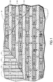
- FIG. 1 a completed conventional stacked-cell DRAM memory array fabricated on a monocrystalline silicon substrate 11 is depicted in a simplified, schematic layout format.
- the array is comprised of a series of parallel, polysilicon wordlines 12 silicided with tungsten, titanium, or other similar refractory metal, the tops of the wordlines being insulated by a first dielectric capping layer (not shown in this view), the sides of the wordlines being insulated by a first set of dielectric spacers 13; a series of bitlines 14, each of which, in the course of its run through the array, makes contact with a multiplicity of heavily doped substrate regions or "active areas" (the areas of bitline-to-substrate contact are rectangular in shape and marked with an "X"); and a multiplicity of storage-node capacitor plates (the rectangular regions marked by a diagonally-cross-hatched pattern) 15.
- Each active area 16 is shared by a pair of cells.
- Each storage node plate 15 makes contact with its associated active area in a storage-node junction region 17, that is identified by a square marked with an "X".
- Each bitline is insulated by a second set of dielectric sidewall spacers 18 and a second dielectric capping layer (not shown in this view). Active areas 16 are separated by field oxide regions, which are not shown in this view.
- FIG. 2A a cross-sectional view of a portion of the DRAM array of Figure 1 through broken line A-A is depicted at a manufacturing stage where active areas 16 and fully-recessed field oxide regions 21 have been created, wordlines 12 have been patterned from a three layer sandwich consisting of a polysilicon-1 layer 22, a silicide layer 23, and a first capping oxide layer 24.
- Active areas 16 consist of lightly-doped junction regions 25, which have been created by implanting phosphorus, and heavily-doped junction regions 26, created by implanting arsenic following the creation of wordline sidewall spacers 27 which resulted from the deposition and anisotropic etch of a first spacer silicon dioxide layer.
- a substrate isolation layer 28 has been conformally deposited.
- the in-process memory array is shown following the deposition of a silicon nitride layer 31 via chemical vapor deposition (CVD), silicon nitride layer 31 being of sufficient thickness to completely fill wordline gaps 32.
- CVD chemical vapor deposition
- the in-process array has received a blanket coating of photoresist 41.
- planarization of the array may be accomplished by any one of a number of known techniques, such as simply utilizing planarizing etch, or spinning photoresist over the array in order to create a planarized surface, then plasma etching the array back to the desired level, or mechanically planarizing the array.
- the in-process array has been masked with a bitline contact photomask 61, and subjected to a plasma etch selective for nitride over oxide in order to remove the portion of nitride filler strip 51 that is exposed by bitline contact photomask 61.
- a plasma etch selective for nitride over oxide in order to remove the portion of nitride filler strip 51 that is exposed by bitline contact photomask 61.
- selectivity as great as 15:1 has been reported in the literature.
- additional plasma etching is utilized.
- FIG. 6B a different cross-sectional view of the in-process DRAM array, taken parallel to and between a pair of wordlines. Visible in this view is substrate isolation layer 28, nitride filler strip 51, and bitline contact photomask 61.
- FIG. 7A the in-process array has been subjected to CVD deposition of a polysilicon-2 layer 71, blanket deposition of a metal silicide layer 72 on top of poly-2 layer 71, and blanket deposition of a silicon dioxide bitline capping layer 73 on top of silicide layer 72.
- Figure 7B a cross-sectional view perpendicular to the cross-sectional view of Figure 7A shows the bit line contact region from a different perspective.
- bitline patterning with bitline photomask 81, and etching to create the individual bitlines has not changed the array cross-section structure through broken line A-A from that of Figure 7A.
- FIG. 8B the effect of the bitline etch is apparent in this cross-sectional view.
- Three individual bitline photomask blocks 81 are visible, as are each of the silicided, oxide-covered bitlines 82.
- Figures 8C and 8D depict different, but process contemporaneous perspectives of the array.
- Figure 9A the in-process array has been subjected to the deposition of a silicon dioxide bitline spacer layer 91.
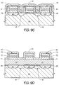
- Figures 9B, 9C and 9D shows a contemporaneous, cross-sectional view through broken line B-B, C-C and D-D, respectively.
- bitline spacer layer 91 which has created bitline sidewall spacers 101 (not shown in this view). Bitline sidewall spacers 101 are visible in Figure 10B.
- the in-process array has been masked with storage node contact photomask 111. Subsequent to this masking step, the array is subjected to a plasma etch selective for silicon nitride over silicon dioxide. The portion of the substrate isolation layer 28 within the storage node contact region is removed with an anisotropic plasma etch selective for oxide.
- Figure 11D gives a different view of this stage of the process.
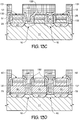
- FIG 12C storage-node contact photomask 111 ha been stripped from the in-process array, and a polysilicon-3 layer 121, from which will be patterned individual storage-node plates, has been blanket deposited.
- Figure 12D gives a different, but contemporaneous perspective of the in-process array.
- polysilicon-3 layer 121 has been patterned with storage node photomask 131 and etched to form individual storage-node capacitor plates 132.
- Figure 13D provides a different, but contemporaneous perspective of the array.
- FIG. 14A storage-node photomask 131 has been stripped from the in-process array, a silicon nitride cell dielectric layer 141 has been blanket deposited over the array surface, and a polysilicon-4 layer 142, from which the cell plate will be formed has been blanket deposited on top of dielectric layer 141.
- Figures 14B, 14C, and 14D provide contemporaneous perspective os the in-process array.
- silicon nitride is considered a superior to silicon dioxide as a cell dielectric material
- the silicon nitride filler strips between the wordlines may replaced by silicon dioxide filler strips.
- silicon nitride would be substituted for all silicon dioxide structures such as wordline and bitline capping dielectric layers, wordline and bitline sidewall spacers, etc.
Landscapes
- Engineering & Computer Science (AREA)
- Manufacturing & Machinery (AREA)
- Semiconductor Memories (AREA)
- Internal Circuitry In Semiconductor Integrated Circuit Devices (AREA)
Applications Claiming Priority (2)
| Application Number | Priority Date | Filing Date | Title |
|---|---|---|---|
| US695182 | 1991-05-03 | ||
| US07/695,182 US5100826A (en) | 1991-05-03 | 1991-05-03 | Process for manufacturing ultra-dense dynamic random access memories using partially-disposable dielectric filler strips between wordlines |
Publications (1)
| Publication Number | Publication Date |
|---|---|
| EP0512463A1 true EP0512463A1 (de) | 1992-11-11 |
Family
ID=24791969
Family Applications (1)
| Application Number | Title | Priority Date | Filing Date |
|---|---|---|---|
| EP92107517A Withdrawn EP0512463A1 (de) | 1991-05-03 | 1992-05-04 | Verfahren zur Herstellung von dynamischer Speichern mit wahlfreiem Zugriff |
Country Status (4)
| Country | Link |
|---|---|
| US (1) | US5100826A (de) |
| EP (1) | EP0512463A1 (de) |
| JP (1) | JP3219850B2 (de) |
| DE (1) | DE512463T1 (de) |
Cited By (1)
| Publication number | Priority date | Publication date | Assignee | Title |
|---|---|---|---|---|
| US5744608A (en) * | 1995-09-08 | 1998-04-28 | Nippon Soda Co., Ltd. | Method for manufacturing 3-(aminomethyl)-6-chloropyridines |
Families Citing this family (20)
| Publication number | Priority date | Publication date | Assignee | Title |
|---|---|---|---|---|
| US5126290A (en) * | 1991-09-11 | 1992-06-30 | Micron Technology, Inc. | Method of making memory devices utilizing one-sided ozone teos spacers |
| KR950011643B1 (ko) * | 1992-04-17 | 1995-10-07 | 현대전자산업주식회사 | 반도체장치 및 그 제조방법 |
| US5480837A (en) * | 1994-06-27 | 1996-01-02 | Industrial Technology Research Institute | Process of making an integrated circuit having a planar conductive layer |
| JP3703885B2 (ja) * | 1995-09-29 | 2005-10-05 | 株式会社東芝 | 半導体記憶装置とその製造方法 |
| KR0161474B1 (ko) * | 1995-12-15 | 1999-02-01 | 김광호 | 셀 플러그 이온주입을 이용한 반도체 메모리장치의 제조방법 |
| JPH10308498A (ja) * | 1997-05-08 | 1998-11-17 | Oki Electric Ind Co Ltd | 半導体装置及びその製造方法 |
| JP3028080B2 (ja) * | 1997-06-18 | 2000-04-04 | 日本電気株式会社 | 半導体装置の構造およびその製造方法 |
| US5917213A (en) * | 1997-08-21 | 1999-06-29 | Micron Technology, Inc. | Depletion compensated polysilicon electrodes |
| US6010935A (en) * | 1997-08-21 | 2000-01-04 | Micron Technology, Inc. | Self aligned contacts |
| US6185473B1 (en) | 1998-01-08 | 2001-02-06 | Micron Technology, Inc. | Optical pattern transfer tool |
| US6373114B1 (en) | 1998-10-23 | 2002-04-16 | Micron Technology, Inc. | Barrier in gate stack for improved gate dielectric integrity |
| US6358788B1 (en) | 1999-08-30 | 2002-03-19 | Micron Technology, Inc. | Method of fabricating a wordline in a memory array of a semiconductor device |
| US6265297B1 (en) | 1999-09-01 | 2001-07-24 | Micron Technology, Inc. | Ammonia passivation of metal gate electrodes to inhibit oxidation of metal |
| US6171948B1 (en) | 1999-11-02 | 2001-01-09 | Micron Technology, Inc. | Method for filling structural gaps and intergrated circuitry |
| US6306767B1 (en) * | 2000-05-31 | 2001-10-23 | Taiwan Semiconductor Manufacturing Company, Ltd | Self-aligned etching method for forming high areal density patterned microelectronic structures |
| US6458714B1 (en) | 2000-11-22 | 2002-10-01 | Micron Technology, Inc. | Method of selective oxidation in semiconductor manufacture |
| US6548347B2 (en) * | 2001-04-12 | 2003-04-15 | Micron Technology, Inc. | Method of forming minimally spaced word lines |
| US11631680B2 (en) | 2018-10-18 | 2023-04-18 | Applied Materials, Inc. | Methods and apparatus for smoothing dynamic random access memory bit line metal |
| US10903112B2 (en) | 2018-10-18 | 2021-01-26 | Applied Materials, Inc. | Methods and apparatus for smoothing dynamic random access memory bit line metal |
| US10700072B2 (en) | 2018-10-18 | 2020-06-30 | Applied Materials, Inc. | Cap layer for bit line resistance reduction |
Citations (4)
| Publication number | Priority date | Publication date | Assignee | Title |
|---|---|---|---|---|
| EP0258657A1 (de) * | 1986-08-22 | 1988-03-09 | Siemens Aktiengesellschaft | Transistorvaraktoranordnung für dynamische Halbleiterspeicher |
| DE3910033A1 (de) * | 1988-03-25 | 1989-10-05 | Toshiba Kawasaki Kk | Halbleiterspeicher und verfahren zu dessen herstellung |
| DE4007582A1 (de) * | 1989-03-09 | 1990-09-13 | Toshiba Kawasaki Kk | Verfahren zum herstellen eines halbleiterbauelements |
| EP0401686A2 (de) * | 1989-05-31 | 1990-12-12 | Nec Corporation | Halbleiter-Speicherzelle mit einer Struktur hoher Dichte |
Family Cites Families (8)
| Publication number | Priority date | Publication date | Assignee | Title |
|---|---|---|---|---|
| JPS60217644A (ja) * | 1984-04-12 | 1985-10-31 | Matsushita Electronics Corp | 半導体装置の製造方法 |
| JPS62210646A (ja) * | 1986-03-11 | 1987-09-16 | Mitsubishi Electric Corp | 半導体装置の製造方法 |
| US4775550A (en) * | 1986-06-03 | 1988-10-04 | Intel Corporation | Surface planarization method for VLSI technology |
| JPS63142A (ja) * | 1986-06-19 | 1988-01-05 | Toshiba Corp | 半導体装置の製造方法 |
| JPS63302537A (ja) * | 1987-06-02 | 1988-12-09 | Rohm Co Ltd | 集積回路の製造方法 |
| US4879257A (en) * | 1987-11-18 | 1989-11-07 | Lsi Logic Corporation | Planarization process |
| KR910009805B1 (ko) * | 1987-11-25 | 1991-11-30 | 후지쓰 가부시끼가이샤 | 다이나믹 랜덤 액세스 메모리 장치와 그의 제조방법 |
| US4894351A (en) * | 1988-02-16 | 1990-01-16 | Sprague Electric Company | Method for making a silicon IC with planar double layer metal conductors system |
-
1991
- 1991-05-03 US US07/695,182 patent/US5100826A/en not_active Expired - Lifetime
-
1992
- 1992-05-04 EP EP92107517A patent/EP0512463A1/de not_active Withdrawn
- 1992-05-04 DE DE92107517T patent/DE512463T1/de active Pending
- 1992-05-06 JP JP15727092A patent/JP3219850B2/ja not_active Expired - Fee Related
Patent Citations (4)
| Publication number | Priority date | Publication date | Assignee | Title |
|---|---|---|---|---|
| EP0258657A1 (de) * | 1986-08-22 | 1988-03-09 | Siemens Aktiengesellschaft | Transistorvaraktoranordnung für dynamische Halbleiterspeicher |
| DE3910033A1 (de) * | 1988-03-25 | 1989-10-05 | Toshiba Kawasaki Kk | Halbleiterspeicher und verfahren zu dessen herstellung |
| DE4007582A1 (de) * | 1989-03-09 | 1990-09-13 | Toshiba Kawasaki Kk | Verfahren zum herstellen eines halbleiterbauelements |
| EP0401686A2 (de) * | 1989-05-31 | 1990-12-12 | Nec Corporation | Halbleiter-Speicherzelle mit einer Struktur hoher Dichte |
Non-Patent Citations (3)
| Title |
|---|
| IEEE TRANSACTIONS ON ELECTRON DEVICES, vol. 38, no. 2, February 1991, New York, US pages 255-261; TORU KAGA et al.: "Crown-shaped stacked-capacitor cell for 1.5-v operation 64-MB drams" * |
| IEEE TRANSACTIONS ON ELECTRON DEVICES. vol. 38, no. 2, February 1991, NEW YORK US pages 255 - 261; TORU KAGA ET AL.: 'CROWN-SHAPED STACKED-CAPACITOR CELL FOR 1.5-V OPERATION 64-MB DRAMS' * |
| PATENT ABSTRACTS OF JAPAN, vol. 15, no. 330 (E-110), 22nd August 1991; & JP-A-31 24 058 (TOSHIBA) 27-05-1991 * |
Cited By (1)
| Publication number | Priority date | Publication date | Assignee | Title |
|---|---|---|---|---|
| US5744608A (en) * | 1995-09-08 | 1998-04-28 | Nippon Soda Co., Ltd. | Method for manufacturing 3-(aminomethyl)-6-chloropyridines |
Also Published As
| Publication number | Publication date |
|---|---|
| JPH077083A (ja) | 1995-01-10 |
| US5100826A (en) | 1992-03-31 |
| DE512463T1 (de) | 1993-10-14 |
| JP3219850B2 (ja) | 2001-10-15 |
Similar Documents
| Publication | Publication Date | Title |
|---|---|---|
| US5100826A (en) | Process for manufacturing ultra-dense dynamic random access memories using partially-disposable dielectric filler strips between wordlines | |
| US5240871A (en) | Corrugated storage contact capacitor and method for forming a corrugated storage contact capacitor | |
| US5990021A (en) | Integrated circuit having self-aligned CVD-tungsten/titanium contact plugs strapped with metal interconnect and method of manufacture | |
| JP3532325B2 (ja) | 半導体記憶装置 | |
| US5700709A (en) | Method for manufacturing a capacitor for a semiconductor device | |
| US6172391B1 (en) | DRAM cell arrangement and method for the manufacture thereof | |
| US5491103A (en) | Method for manufacturing a capacitor structure of a semiconductor memory device | |
| EP0318277B1 (de) | Dynamische Speicheranordnung mit wahlfreiem Zugriff und Herstellungsverfahren dafür | |
| US5150276A (en) | Method of fabricating a vertical parallel cell capacitor having a storage node capacitor plate comprising a center fin effecting electrical communication between itself and parallel annular rings | |
| US5137842A (en) | Stacked H-cell capacitor and process to fabricate same | |
| US5733809A (en) | Split-polysilicon CMOS process for multi-megabit dynamic memories incorporating stacked container capacitor cells | |
| US6162676A (en) | Method of making a semiconductor device with an etching stopper | |
| JP2608363B2 (ja) | 半導体メモリ装置及びその製造方法 | |
| US5371701A (en) | Stacked delta cell capacitor | |
| KR100373297B1 (ko) | 반도체 장치 및 그 제조 방법 | |
| EP0601868A1 (de) | Halbleiter-Speicherbauteil | |
| US6069038A (en) | Method of manufacturing a semiconductor integrated circuit device | |
| US6686288B1 (en) | Integrated circuit having self-aligned CVD-tungsten/titanium contact plugs strapped with metal interconnect and method of manufacture | |
| US5005072A (en) | Stacked cell design for 16-megabit DRAM array having a pair of interconnected poly layers which enfold a single field plate layer and connect to the cell's storage node junction | |
| US6174767B1 (en) | Method of fabrication of capacitor and bit-line at same level for 8F2 DRAM cell with minimum bit-line coupling noise | |
| KR20020042420A (ko) | 메모리 어레이 및 지원 트랜지스터 형성 방법 | |
| US5409855A (en) | Process for forming a semiconductor device having a capacitor | |
| US5571742A (en) | Method of fabricating stacked capacitor of DRAM cell | |
| KR100448719B1 (ko) | 다마신공정을 이용한 반도체 장치 및 그의 제조방법 | |
| US6228711B1 (en) | Method of fabricating dynamic random access memory |
Legal Events
| Date | Code | Title | Description |
|---|---|---|---|
| PUAI | Public reference made under article 153(3) epc to a published international application that has entered the european phase |
Free format text: ORIGINAL CODE: 0009012 |
|
| AK | Designated contracting states |
Kind code of ref document: A1 Designated state(s): DE |
|
| 17P | Request for examination filed |
Effective date: 19930510 |
|
| DET | De: translation of patent claims | ||
| STAA | Information on the status of an ep patent application or granted ep patent |
Free format text: STATUS: THE APPLICATION IS DEEMED TO BE WITHDRAWN |
|
| 18D | Application deemed to be withdrawn |
Effective date: 19941201 |