EP0318277B1 - Dynamische Speicheranordnung mit wahlfreiem Zugriff und Herstellungsverfahren dafür - Google Patents
Dynamische Speicheranordnung mit wahlfreiem Zugriff und Herstellungsverfahren dafür Download PDFInfo
- Publication number
- EP0318277B1 EP0318277B1 EP88311107A EP88311107A EP0318277B1 EP 0318277 B1 EP0318277 B1 EP 0318277B1 EP 88311107 A EP88311107 A EP 88311107A EP 88311107 A EP88311107 A EP 88311107A EP 0318277 B1 EP0318277 B1 EP 0318277B1
- Authority
- EP
- European Patent Office
- Prior art keywords
- film
- insulation film
- forming
- bit lines
- insulation
- Prior art date
- Legal status (The legal status is an assumption and is not a legal conclusion. Google has not performed a legal analysis and makes no representation as to the accuracy of the status listed.)
- Expired - Lifetime
Links
Images


Classifications
-
- H—ELECTRICITY
- H10—SEMICONDUCTOR DEVICES; ELECTRIC SOLID-STATE DEVICES NOT OTHERWISE PROVIDED FOR
- H10B—ELECTRONIC MEMORY DEVICES
- H10B12/00—Dynamic random access memory [DRAM] devices
- H10B12/30—DRAM devices comprising one-transistor - one-capacitor [1T-1C] memory cells
- H10B12/48—Data lines or contacts therefor
- H10B12/482—Bit lines
-
- H—ELECTRICITY
- H10—SEMICONDUCTOR DEVICES; ELECTRIC SOLID-STATE DEVICES NOT OTHERWISE PROVIDED FOR
- H10B—ELECTRONIC MEMORY DEVICES
- H10B12/00—Dynamic random access memory [DRAM] devices
- H10B12/01—Manufacture or treatment
- H10B12/02—Manufacture or treatment for one transistor one-capacitor [1T-1C] memory cells
- H10B12/03—Making the capacitor or connections thereto
- H10B12/033—Making the capacitor or connections thereto the capacitor extending over the transistor
-
- H—ELECTRICITY
- H10—SEMICONDUCTOR DEVICES; ELECTRIC SOLID-STATE DEVICES NOT OTHERWISE PROVIDED FOR
- H10B—ELECTRONIC MEMORY DEVICES
- H10B12/00—Dynamic random access memory [DRAM] devices
- H10B12/30—DRAM devices comprising one-transistor - one-capacitor [1T-1C] memory cells
- H10B12/31—DRAM devices comprising one-transistor - one-capacitor [1T-1C] memory cells having a storage electrode stacked over the transistor
-
- Y—GENERAL TAGGING OF NEW TECHNOLOGICAL DEVELOPMENTS; GENERAL TAGGING OF CROSS-SECTIONAL TECHNOLOGIES SPANNING OVER SEVERAL SECTIONS OF THE IPC; TECHNICAL SUBJECTS COVERED BY FORMER USPC CROSS-REFERENCE ART COLLECTIONS [XRACs] AND DIGESTS
- Y10—TECHNICAL SUBJECTS COVERED BY FORMER USPC
- Y10S—TECHNICAL SUBJECTS COVERED BY FORMER USPC CROSS-REFERENCE ART COLLECTIONS [XRACs] AND DIGESTS
- Y10S257/00—Active solid-state devices, e.g. transistors, solid-state diodes
- Y10S257/90—MOSFET type gate sidewall insulating spacer
Definitions
- DRAM device Two basic types of DRAM device are referred to as the "open bit-line type” and the “folded bit-line type” respectively.
- JP-A-59 231851 by Nippon Denshin Denwa Kosha discloses a similar type of DRAM device, also of the open bit-line type.
- a dynamic random access memory device comprising:- a semiconductor substrate having source regions and drain regions; a gate insulation film formed on a surface of the semiconductor substrate; a plurality of word lines and gate electrodes formed over the surface of the semiconductor substrate via the gate insulation film, the word lines being connected to the gate electrodes; and a second insulation film formed so as to cover the word lines and gate electrodes; a plurality of bit lines formed on the second insulation film, intersections being formed at cross points of the word lines and the bit lines, a bit line contacting one of the source regions via a first opening formed in the gate insulation film and second insulation film; a third insulation film formed so as to cover the bit lines; storage electrodes formed over the third insulation film and contacting respective drain regions via second openings formed in the gate insulation film and the second and third insulation films, the bit lines being located at a layer level lower than the storage electrodes; a dielectric film formed so as to surround the storage electrodes; and an opposed electrode provided for each storage electrode, formed so as to
- a method for producing a dynamic random access memory device comprising the steps of:- forming word lines and gate electrodes on a gate insulation film formed on a semiconductor substrate and source and drain regions in the semiconductor substrate, the word lines being connected to the gate electrodes; forming a second insulation film so as to cover the word lines and gate electrodes; forming first openings in the gate insulation film and second insulation film; forming bit lines crossing the word lines so as to form intersections at cross points of the word lines and bit lines, the bit lines contacting the source regions through the first openings and overlying the second insulation film; forming a third insulation film so as to cover the bit lines; forming second openings in the gate insulation film and the second and third insulation films; forming storage electrodes in contact with respective drain regions through the second openings and overlying the third insulation film; forming a dielectric film so as to surround the storage electrodes; and forming, for each storage electrode, an opposed electrode which covers the dielectric film; characterised by forming said first opening
- An embodiment of the present invention also provides a random access memory device in which neighbouring bit lines are electrically shielded very well.
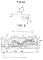
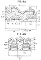
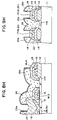
- FIGS.1A and 1B Before describing the preferred embodiments of the present invention, a description is given of a memory cell for a conventional DRAM device with reference to FIGS.1A and 1B.
- FIG.1A is a circuit diagram of a memory cell for a DRAM device.
- a memory cell is composed of a transfer gate transistor T and a memory cell capacitor C.
- a source of the transfer gate transistor T is connected to a corresponding bit line BL, and a drain thereof is connected to a storage electrode 6.
- a gate of the transfer gate transistor T is connected to a corresponding word line WL.
- An opposed electrode 8 is connected to a constant power source.
- a dielectric film 7 is provided between the storage electrode 6 and the opposed electrode 8.
- FIG.1B shows a cross section of a conventional layer structure which provides the memory cell of FIG.1A.
- the memory cell comprises a p-type silicon substrate 1, a field insulation film 2, a gate insulation film 3, a drain region 4D, a source region 4S, and a silicon dioxide film 5.
- the gate electrode WL1 is concerned with the transfer gate transistor T, and the gate electrode WL2 is concerned with another transfer gate transistor (not shown).
- Gate electrodes WL1 and WL2 of polysilicon are formed on the gate insulation film 3 and the silicon dioxide film 5, respectively.
- the storage electrode 6 is formed so as to be in contact with the drain region 4D.
- the dielectric film 7 is formed so as to surround the storage electrode 6.
- the dielectric film 7 is covered with the opposed electrode 8.
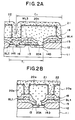
- each bit line BL1 has a layer level lower than that of the storage electrode 20a. Therefore, it is unnecessary to form bit lines on an insulation film which covers the memory cell capacitor. Additionally, it becomes possible to increase the storage electrode 20a because there is no bit line contact hole in the insulation film which covers the memory cell capacitor. As a result, the storage electrode 20a thicker than that of the storage electrode 6 shown in FIG.1B can be formed. It is noted that the thicker storage electrode 20a increases the capacitance of the memory cell capacitor. In the case where each bit line has a layer level higher than that of the storage electrode as in the case of the conventional DRAM device of FIG.1B, there is a limit on the film thickness of the storage electrode 6. This is because the presence of a thick storage electrode in the conventional layer structure makes it difficult to make contacts between the source regions 3S and the bit lines BL.
- the adjacent bit lines BL1 of the FIG.2 device are electrically shielded by the storage electrode 20a and opposed electrode 22 interposed therebetween.
- the storage electrode 20a is normally in a floating state, there exists the strong capacitive coupling between the storage electrode 20a and the opposed electrode 22.
- the storage electrode 20a can function as an electrical shield member with respect to the neighboring bit lines BL1. With the above structure, it becomes possible to reduce noise introduced on the bit lines BL1.
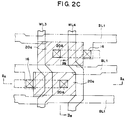
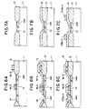
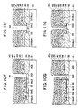
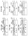
- FIGS.3A through 3C A description is given of a second DRAM device useful for understanding the present invention with reference to FIGS.3A through 3C.
- FIGS.3A through 3C those parts which are the same as those in the previous figures, are given the same reference numerals.
- FIGS.3A and 3B are cross sectional views taken along the lines III A -III A and III B -III B of FIG.3C, respectively.
- This device is composed of a transfer gate transistor T2 and a memory cell capacitor C2, as in the case of the first device (FIG.2).
- the second device is different from the first device in position of bit line contact holes.
- each bit line contact hole 16 and the corresponding storage electrode contact hole 20A are aligned in the direction of extension of the bit lines BL1.
- the bit line contact hole 16 is positioned in the center of a distance between the neighboring bit lines BL1.
- a bit line contact hole 16a with respect to a bit line BL22 and the corresponding storage electrode contact hole 20A of the transfer gate transistor T2 are not arranged into a line.
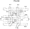
- FIGS.4A and 4B are cross sectional views taken along the lines IV A -IV A and IV B -IV B of FIG.4C, respectively.
- the device is composed of a transfer gate transistor T3 and a memory cell capacitor C3.
- the transfer gate transistor T3 comprises the source and drain regions 14S and 14D, the gate electrode 13 and a bit line BL32.
- the memory cell capacitor C3 comprises a storage electrode 25a of polysilicon, a dielectric film 26 of silicon dioxide, and an opposed electrode 27 of polysilicon.
- the storage electrode 25a and the opposed electrode 27 are doped with n+-type impurity such as arsenic (As) and phosphorus (P), respectively.
- This device has an essential feature in which it has a storage electrode contact hole 24 which is formed in an insulation film by a self-alignment process in which bit lines BL31, BL32 and BL33 function as a resist mask film. As shown in FIG.4C, the storage electrode contact hole 24 has a slit shape. By the self-alignment process, it is unnecessary to carry out a positioning operation with respect to the storage electrode contact holes 24. Additionally, a decreased area of the memory cell which occupies the silicon substrate 11, is obtainable.
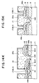
- the interlayer insulation film 15 of silicon dioxide is deposited to a thickness of approximately 1000 [ ⁇ ] so as to cover the gate electrodes WL3 and WL4. Then the interlayer insulation film 15 is etched by an anisotropic etching process such as RIE so as to form the opening (bit line contact hole) 16. In the RIE process, an etching gas of CHF3 + H2 is used.
- a polysilicon film 20 is deposited by chemical vapor deposition on the entire surface of the silicon substrate 11, and is then patterned by anisotropic etching such as RIE so as to form the storage electrodes 20a.
- the polysilicon film 20 is approximately 4000 [ ⁇ ] thick.
- An etching gas of CCl4/O2 is used in the anisotropic etching process.
- the silicon dioxide film 23 having a thickness of approximately 1000 [ ⁇ ] is deposited on the entire surface of the silicon substrate 11 by chemical vapor deposition.
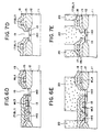
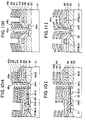
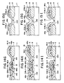
- FIGS.10A through 10J A description is given of a method according to the second aspect of the invention, for producing a device of the first aspect, with reference to FIGS.10A through 10J, and FIGS.11A through 11J.
- the interlayer insulation film 35 of silicon dioxide is deposited on the entire surface of the silicon substrate 31.
- the opening 36 is formed in the interlayer insulation film 35 and the gate insulation film 33 by anisotropic etching such as RIE in which an etching gas of CHF3 + H2 is used.
- the opening 36 functions as the bit line contact hole.
- a polysilicon film 45c is deposited on the entire surface of the silicon substrate 31 by low-pressure chemical vapor deposition. Thereby the top and side surfaces of a stacked layer composed of the silicon dioxide and polysilicon films are covered with the polysilicon film 45c.
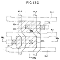
- FIGS.13A through 13C those parts which are the same as those in FIGS.2A through 2C, are indicated by the same reference numerals.
- the insulation film 18 and the interlayer insulation film 15 are selectively etched so as to form the opening 19 through which a surface of the drain region 14D is exposed.
- the opening 19 functions as the storage electrode contact hole.
Landscapes
- Engineering & Computer Science (AREA)
- Manufacturing & Machinery (AREA)
- Semiconductor Memories (AREA)
Claims (12)
- Dynamische Direktzugriffsspeichervorrichtung, enthaltend:
ein Halbleitersubstrat (11, 31), das Source-Bereiche (14S, 34S) und Drain-Bereiche (14D, 34D) hat,
einen Gate-Isolationsfilm (13, 33), der auf einer Oberfläche des Halbleitersubstrats ausgebildet ist,
eine Mehrzahl von Wortleitungen (WL3, WL5) und Gate-Elektroden, die auf der Oberfläche des Halbleitersubstrats über dem Gate-Isolationsfilm ausgebildet sind, wobei die Wortleitungen mit den Gate-Elektroden verbunden sind, un
einen zweiten Isolationsfilm (15, 35), der so ausgebildet ist, daß er die Wortleitungen und Gate-Elektroden bedeckt,
eine Mehrzahl von Bitleitungen (BL1, BL22, BL32, BL4), die auf dem zweiten Isolationsfilm ausgebildet sind, wobei Knoten an Kreuzungspunkten der Wortleitungen und Bitleitungen ausgebildet sind, und wobei eine Bitleitung mit einem der Source-Bereiche über eine erste Öffnung in Kontakt ist, die im Gate-Isolationsfilm und im zweiten Isolationsfilm ausgebildet ist,
einen dritten Isolationsfilm (18, 23, 38), der so ausgebildet ist, daß er die Bitleitungen bedeckt,
Speicherelektroden (20a, 25a, 45), die auf dem dritten Isolationsfilm ausgebildet sind und über zweite Öffnungen (20A, 24, 44), die in dem Gate-Isolationsfilm und den zweiten und dritten Isolationsfilmen ausgebildet sind, mit jeweiligen Drain-Bereichen in Kontakt sind, wobei die Bitleitungen auf einem niedrigeren Schichtniveau als die Speicherelektroden angeordnet sind,
einen dielektrischen Film, der so ausgebildet ist, daß er die Speicherelektroden umgibt, und
eine für jede Speicherelektrode vorgesehene Gegenelektrode, die so ausgebildet ist, daß sie den dielektrischen Film bedeckt,
dadurch gekennzeichnet,
daß die ersten Öffnungen nur an einem von zwei Kreuzungspunkten bestehen, die durch jede der Wortleitungen und jedes Paar benachbarter Bitleitungen gebildet werden, und
daß jede Gegenelektrode einen Bereich hat, der zwischen einer unteren Oberfläche ihrer jeweiligen Speicherelektrode und dem dritten Isolationsfilm angeordnet ist. - Vorrichtung nach Anspruch 1, dadurch gekennzeichnet, daß die ersten Öffnungen (16, 16a, 36) und die zweiten Öffnungen (20A, 24, 44) in der Erstreckungsrichtung der Bitleitungen (BL1, BL22, BL32, BL4) ausgerichtet sind.
- Vorrichtung nach Anspruch 1, dadurch gekennzeichnet, daß die Bitleitungen (BL1, BL22, BL32, BL4) einen aus einem polykristallinen Siliziumfilm bestehenden Polyzidfilm und einen höchstschmelzenden Metallfilm enthalten, der aus dem polykristallinen Siliziumfilm gebildet ist.
- Vorrichtung nach Anspruch 1, dadurch gekennzeichnet, daß ein Isolations-Seitenwandfilm (49a) mit einem abfallenden Querschnittsbereich so ausgebildet ist, daß er eine Seitenwand der Bitleitungen (BL1) umgibt.
- Vorrichtung nach Anspruch 1, dadurch gekennzeichnet, daß ein Isolations-Seitenwandfilm (48a) mit einem abfallenden Querschnittsbereich so ausgebildet ist, daß er eine Seitenwand der Wortleitungen (WL3) und Gate-Elektroden umgibt.
- Vorrichtung nach Anspruch 1, dadurch gekennzeichnet, daß jede Speicherelektrode (45) einen Vertikalbereich (45a), der in Kontakt mit dem Drain-Bereich (34D) ist, und Flügelbereiche (45b) enthält, die durch eine Lücke voneinander getrennt und mit dem Vertikalbereich (45a) verbunden sind.
- Vorrichtung nach Anspruch 6, dadurch gekennzeichnet, daß sich die Flügelbereiche der Speicherelektroden über die Wortleitungen erstrecken.
- Verfahren zum Herstellen einer dynamischen Direktzugriffsspeichervorrichtung, enthaltend die Schritte:
Ausbilden von Wortleitungen (WL3, WL5) und Gate-Elektroden auf einem Gate-Isolationsfilm (13, 33), der auf einem Halbleitersubstrat und Source- und Drain-Bereichen (14S, 14D, 34S, 34D) in dem Halbleitersubstrat ausgebildet ist, wobei die Wortleitungen mit den Gate-Elektroden verbunden werden,
Ausbilden eines zweiten Isolationsfilms (15, 35), so daß er die Wortleitungen und Gate-Elektroden bedeckt,
Ausbilden erster Öffnungen (16, 16a, 36) im Gate-Isolationsfilm und im zweiten Isolationsfilm,
Ausbilden von Bitleitungen (BL1, BL22, BL32, BL4), die die Wortleitungen kreuzen, so daß sie Knoten an den Kreuzungspunkten der Wortleitungen und Bitleitungen bilden, wobei die Bitleitungen mit den Source-Bereichen durch die ersten Öffnungen im Kontakt sind und auf dem zweiten Isolationsfilm liegen,
Ausbilden eines dritten Isolationsfilms (18, 23, 38), so daß er die Bitleitungen bedeckt,
Ausbilden zweiter Öffnungen (20A, 24, 44) im Gate-Isolationsfilm und in den zweiten und dritten Isolationsfilmen,
Ausbilden von Speicherelektroden (20a, 25a, 45), die durch die zweiten Öffnungen mit jeweiligen Drain-Bereichen in Kontakt sind und auf dem dritten Isolationsfilm liegen,
Ausbilden eines dielektrischen Films (21, 26, 46), so daß er die Speicherelektroden umgibt, und Ausbilden einer Gegenelektrode (22, 27, 47), die den dielektrischen Film bedeckt, für jede Speicherelektrode,
gekennzeichnet durch Ausbilden der ersten Öffnungen an nur einem von zwei Kreuzungspunkten, die von jeder der Wortleitungen und jedem Paar benachbarter Bitleitungen gebildet werden, und Ausbilden jeder Gegenelektrode mit einem Bereich, der zwischen einer unteren Oberfläche ihrer entsprechenden Speicherelektrode und dem dritten Isolationsfilm angeordnet ist. - Verfahren nach Anspruch 8, dadurch gekennzeichnet, daß der Schritt des Ausbildens der Speicherelektroden (45) die Schritte des Ausbildens eines Isolationsfilms (39) auf dem dritten Isolationsfilm (38) und des Ausbildens eines leitenden Films (40) auf den Isolationsfilm (39) enthält, und die Schritte des Ausbildens des Isolationsfilms und des Ausbildens des leitenden Films werden jeweils repetitiv so ausgeführt, daß sie eine Stapelschichtstruktur bilden, die aus einer Mehrzahl von Isolationsfilmen (39, 41, 43) und leitenden Filmen (40, 42, 45c) besteht.
- Verfahren nach Anspruch 9, dadurch gekennzeichnet, daß der Schritt des Ausbildens der Speicherelektroden (45), ferner die Schritte des Musterns der Mehrzahl von leitenden und Isolationsfilmen (39 bis 43, 45c) durch einen anisotropen Ätzprozeß und des Entfernens gemusterter Isolationsfilme (39, 41, 43) durch einen isotropen Ätzprozeß enthält.
- Verfahren nach Anspruch 8, ferner gekennzeichnet durch die Schritte des Ausbildens eines vierten Isolationsfilms (48) zum Bedecken der Wortleitungen (WL3) und des Musterns des vierten Isolationsfilms durch einen anisotropen Ätzprozeß, so daß ein einen abfallenden Querschnitt aufweisender Bereich (48a) des vierten Isolationsfilms um die Wortleitungen und Gate-Elektroden herum belassen wird und als ein Seitenwandfilm fungiert.
- Verfahren nach Anspruch 8, ferner gekennzeichnet durch die Schritte des Ausbildens eines fünften Isolationsfilms (49) zum Bedecken der Bitleitungen und Musterns des fünften Isolationsfilms durch einen anisotropen Ätzprozeß, so daß ein einen abfallenden Querschnitt aufweisender Bereich (49a) des fünften Isolationsfilms um die Bitleitungen belassen wird und als ein Seitenwandfilm fungiert.
Priority Applications (1)
| Application Number | Priority Date | Filing Date | Title |
|---|---|---|---|
| EP95102886A EP0661752B1 (de) | 1987-11-25 | 1988-11-24 | Dynamische Spreicheranordnung mit wahlfreiem Zugriff und Herstellungsverfahren dafür |
Applications Claiming Priority (4)
| Application Number | Priority Date | Filing Date | Title |
|---|---|---|---|
| JP62296669A JP2772375B2 (ja) | 1987-11-25 | 1987-11-25 | 半導体記憶装置 |
| JP296669/87 | 1987-11-25 | ||
| JP62302464A JPH07118520B2 (ja) | 1987-11-30 | 1987-11-30 | 半導体記憶装置及びその製造方法 |
| JP302464/87 | 1987-11-30 |
Related Child Applications (2)
| Application Number | Title | Priority Date | Filing Date |
|---|---|---|---|
| EP95102886A Division EP0661752B1 (de) | 1987-11-25 | 1988-11-24 | Dynamische Spreicheranordnung mit wahlfreiem Zugriff und Herstellungsverfahren dafür |
| EP95102886.9 Division-Into | 1988-11-24 |
Publications (3)
| Publication Number | Publication Date |
|---|---|
| EP0318277A2 EP0318277A2 (de) | 1989-05-31 |
| EP0318277A3 EP0318277A3 (en) | 1990-10-31 |
| EP0318277B1 true EP0318277B1 (de) | 1995-09-06 |
Family
ID=26560793
Family Applications (2)
| Application Number | Title | Priority Date | Filing Date |
|---|---|---|---|
| EP88311107A Expired - Lifetime EP0318277B1 (de) | 1987-11-25 | 1988-11-24 | Dynamische Speicheranordnung mit wahlfreiem Zugriff und Herstellungsverfahren dafür |
| EP95102886A Expired - Lifetime EP0661752B1 (de) | 1987-11-25 | 1988-11-24 | Dynamische Spreicheranordnung mit wahlfreiem Zugriff und Herstellungsverfahren dafür |
Family Applications After (1)
| Application Number | Title | Priority Date | Filing Date |
|---|---|---|---|
| EP95102886A Expired - Lifetime EP0661752B1 (de) | 1987-11-25 | 1988-11-24 | Dynamische Spreicheranordnung mit wahlfreiem Zugriff und Herstellungsverfahren dafür |
Country Status (4)
| Country | Link |
|---|---|
| US (5) | US4953126A (de) |
| EP (2) | EP0318277B1 (de) |
| KR (1) | KR910009805B1 (de) |
| DE (2) | DE3856543T2 (de) |
Families Citing this family (82)
| Publication number | Priority date | Publication date | Assignee | Title |
|---|---|---|---|---|
| KR910009805B1 (ko) * | 1987-11-25 | 1991-11-30 | 후지쓰 가부시끼가이샤 | 다이나믹 랜덤 액세스 메모리 장치와 그의 제조방법 |
| US5374576A (en) * | 1988-12-21 | 1994-12-20 | Hitachi, Ltd. | Method of fabricating stacked capacitor cell memory devices |
| US20010008288A1 (en) * | 1988-01-08 | 2001-07-19 | Hitachi, Ltd. | Semiconductor integrated circuit device having memory cells |
| JP2755591B2 (ja) * | 1988-03-25 | 1998-05-20 | 株式会社東芝 | 半導体記憶装置 |
| JP2838412B2 (ja) * | 1988-06-10 | 1998-12-16 | 三菱電機株式会社 | 半導体記憶装置のキャパシタおよびその製造方法 |
| US5091761A (en) * | 1988-08-22 | 1992-02-25 | Hitachi, Ltd. | Semiconductor device having an arrangement of IGFETs and capacitors stacked thereover |
| JPH02156566A (ja) * | 1988-12-08 | 1990-06-15 | Mitsubishi Electric Corp | 半導体記憶装置およびその製造方法 |
| US5219781A (en) * | 1988-12-08 | 1993-06-15 | Mitsubishi Denki Kabushiki Kaisha | Method for manufacturing semiconductor memory device having a stacked type capacitor |
| US5162249A (en) * | 1989-04-03 | 1992-11-10 | Hyundai Electronics Industries Co., Ltd. | Method of making semiconductor memory device having a double stacked capacitor |
| US5059548A (en) * | 1989-04-03 | 1991-10-22 | Hyundai Electronics Industries Co., Ltd. | Method of making a semiconductor memory device having a double stacked capacitor |
| JPH0824169B2 (ja) * | 1989-05-10 | 1996-03-06 | 富士通株式会社 | 半導体記憶装置の製造方法 |
| US5196365A (en) * | 1989-07-05 | 1993-03-23 | Fujitsu Limited | Method of making semiconductor memory device having stacked capacitor |
| JP2974252B2 (ja) * | 1989-08-19 | 1999-11-10 | 富士通株式会社 | 半導体記憶装置 |
| US5196909A (en) * | 1989-11-30 | 1993-03-23 | Sgs-Thomson Microelectronics, Inc. | Capacitor for DRAM cell |
| JP2528719B2 (ja) * | 1989-12-01 | 1996-08-28 | 三菱電機株式会社 | 半導体記憶装置 |
| EP1465248A1 (de) * | 1990-03-08 | 2004-10-06 | Fujitsu Limited | Schichtstruktur mit Kontaktloch und Verfahren zur Herstellung derselben |
| US5240872A (en) * | 1990-05-02 | 1993-08-31 | Mitsubishi Denki Kabushiki Kaisha | Method of manufacturing semiconductor device having interconnection layer contacting source/drain regions |
| JP2934325B2 (ja) * | 1990-05-02 | 1999-08-16 | 三菱電機株式会社 | 半導体装置およびその製造方法 |
| JP2746730B2 (ja) * | 1990-05-17 | 1998-05-06 | 富士通株式会社 | 半導体記憶装置 |
| JP2504606B2 (ja) * | 1990-05-18 | 1996-06-05 | 株式会社東芝 | 半導体記憶装置およびその製造方法 |
| KR930007192B1 (ko) * | 1990-06-29 | 1993-07-31 | 삼성전자 주식회사 | 디램셀의 적층형캐패시터 및 제조방법 |
| KR920001760A (ko) * | 1990-06-29 | 1992-01-30 | 김광호 | 디램셀의 적층형 캐패시터 제조방법 |
| US5219778A (en) * | 1990-10-16 | 1993-06-15 | Micron Technology, Inc. | Stacked V-cell capacitor |
| US5236855A (en) * | 1990-11-06 | 1993-08-17 | Micron Technology, Inc. | Stacked V-cell capacitor using a disposable outer digit line spacer |
| US5049517A (en) * | 1990-11-07 | 1991-09-17 | Micron Technology, Inc. | Method for formation of a stacked capacitor |
| JPH04181769A (ja) * | 1990-11-15 | 1992-06-29 | Matsushita Electric Ind Co Ltd | 半導体記憶装置およびその製造方法 |
| US6002149A (en) * | 1990-11-19 | 1999-12-14 | Micron Technology, Inc. | Capacitor structures for memory cells |
| KR930009594B1 (ko) * | 1991-01-30 | 1993-10-07 | 삼성전자 주식회사 | 고집적 반도체 메모리장치 및 그 제조방법 |
| KR920017248A (ko) * | 1991-02-18 | 1992-09-26 | 문정환 | 반도체 메모리 소자의 커패시터 제조방법 |
| US5053351A (en) * | 1991-03-19 | 1991-10-01 | Micron Technology, Inc. | Method of making stacked E-cell capacitor DRAM cell |
| US5100826A (en) * | 1991-05-03 | 1992-03-31 | Micron Technology, Inc. | Process for manufacturing ultra-dense dynamic random access memories using partially-disposable dielectric filler strips between wordlines |
| KR930010081B1 (ko) * | 1991-05-24 | 1993-10-14 | 현대전자산업 주식회사 | 2중 적층캐패시터 구조를 갖는 반도체 기억장치 및 그 제조방법 |
| US5084406A (en) * | 1991-07-01 | 1992-01-28 | Micron Technology, Inc. | Method for forming low resistance DRAM digit-line |
| EP0782195B1 (de) * | 1991-07-25 | 1999-10-13 | Fujitsu Limited | Herstellungsverfahren für Kondensator mit gestapelter Flossenstruktur und mit reduzierter Flossendicke |
| TW301782B (de) * | 1991-08-16 | 1997-04-01 | Gold Star Electronics | |
| US5231043A (en) * | 1991-08-21 | 1993-07-27 | Sgs-Thomson Microelectronics, Inc. | Contact alignment for integrated circuits |
| TW243541B (de) * | 1991-08-31 | 1995-03-21 | Samsung Electronics Co Ltd | |
| JPH0582747A (ja) * | 1991-09-19 | 1993-04-02 | Fujitsu Ltd | 半導体装置 |
| US5573967A (en) * | 1991-12-20 | 1996-11-12 | Industrial Technology Research Institute | Method for making dynamic random access memory with fin-type stacked capacitor |
| US5208172A (en) * | 1992-03-02 | 1993-05-04 | Motorola, Inc. | Method for forming a raised vertical transistor |
| US5525534A (en) * | 1992-03-13 | 1996-06-11 | Fujitsu Limited | Method of producing a semiconductor device using a reticle having a polygonal shaped hole |
| KR0121297B1 (en) * | 1992-04-16 | 1997-11-15 | Fujitsu Ltd | Semiconductor device and process of producing the same |
| US5591659A (en) * | 1992-04-16 | 1997-01-07 | Fujitsu Limited | Process of producing a semiconductor device in which a height difference between a memory cell area and a peripheral area is eliminated |
| KR960003498B1 (ko) * | 1992-06-18 | 1996-03-14 | 금성일렉트론주식회사 | 반도체장치의 캐패시터 제조방법 |
| TW227628B (de) * | 1992-12-10 | 1994-08-01 | Samsung Electronics Co Ltd | |
| GB2278907A (en) * | 1993-06-08 | 1994-12-14 | Vinten Group Plc | Manual control system for camera mountings |
| US5648290A (en) * | 1994-12-30 | 1997-07-15 | Lsi Logic Corporation | Method of making a CMOS dynamic random-access memory (DRAM) |
| US5959319A (en) * | 1995-04-18 | 1999-09-28 | Nippon Steel Corporation | Semiconductor memory device having word line conductors provided at lower level than memory cell capacitor and method of manufacturing same |
| US5807782A (en) * | 1995-09-25 | 1998-09-15 | Vanguard International Semiconductor Corporation | Method of manufacturing a stacked capacitor having a fin-shaped storage electrode on a dynamic random access memory cell |
| US5783470A (en) * | 1995-12-14 | 1998-07-21 | Lsi Logic Corporation | Method of making CMOS dynamic random-access memory structures and the like |
| US5604146A (en) * | 1996-06-10 | 1997-02-18 | Vanguard International Semiconductor Corporation | Method to fabricate a semiconductor memory device having an E-shaped storage node |
| TW312831B (en) * | 1996-08-16 | 1997-08-11 | United Microelectronics Corp | Manufacturing method of semiconductor memory device with capacitor(3) |
| US5759890A (en) * | 1996-08-16 | 1998-06-02 | United Microelectronics Corporation | Method for fabricating a tree-type capacitor structure for a semiconductor memory device |
| TW306064B (en) * | 1996-08-16 | 1997-05-21 | United Microelectronics Corp | Semiconductor memory device with capacitor (part 6) |
| TW366592B (en) * | 1996-08-16 | 1999-08-11 | United Microelectronics Corp | DRAM memory and the manufacturing method for the memory cells |
| TW427012B (en) * | 1996-08-16 | 2001-03-21 | United Microelectronics Corp | The manufacturing method of double-combined capacitor DRAM cells |
| TW308727B (en) * | 1996-08-16 | 1997-06-21 | United Microelectronics Corp | Semiconductor memory device with capacitor (4) |
| US5796138A (en) * | 1996-08-16 | 1998-08-18 | United Microelectronics Corporation | Semiconductor memory device having a tree type capacitor |
| TW302524B (en) * | 1996-08-16 | 1997-04-11 | United Microelectronics Corp | Memory cell structure of dynamic random access memory and manufacturing method thereof |
| TW312829B (en) * | 1996-08-16 | 1997-08-11 | United Microelectronics Corp | Semiconductor memory device with capacitor(6) |
| US5739060A (en) * | 1996-08-16 | 1998-04-14 | United Microelecrtronics Corporation | Method of fabricating a capacitor structure for a semiconductor memory device |
| TW308729B (en) * | 1996-08-16 | 1997-06-21 | United Microelectronics Corp | Semiconductor memory device with capacitor (3) |
| TW304288B (en) * | 1996-08-16 | 1997-05-01 | United Microelectronics Corp | Manufacturing method of semiconductor memory device with capacitor |
| US5811848A (en) * | 1996-08-16 | 1998-09-22 | United Microelectronics Corporation | Capacitor structure for a semiconductor memory device |
| TW351846B (en) * | 1996-08-16 | 1999-02-01 | United Microelectronics Corp | Method for fabricating memory cell for DRAM |
| TW312828B (en) * | 1996-08-16 | 1997-08-11 | United Microelectronics Corp | Manufacturing method of semiconductor memory device with capacitor(5) |
| TW306036B (en) * | 1996-08-16 | 1997-05-21 | United Microelectronics Corp | Semiconductor memory device with capacitor (part 2) |
| TW304290B (en) * | 1996-08-16 | 1997-05-01 | United Microelectronics Corp | The manufacturing method for semiconductor memory device with capacitor |
| US5744833A (en) * | 1996-08-16 | 1998-04-28 | United Microelectronics Corporation | Semiconductor memory device having tree-type capacitor |
| TW297948B (en) * | 1996-08-16 | 1997-02-11 | United Microelectronics Corp | Memory cell structure of DRAM |
| JP3373134B2 (ja) * | 1997-06-13 | 2003-02-04 | 沖電気工業株式会社 | 半導体装置の製造方法 |
| US6146962A (en) * | 1998-03-17 | 2000-11-14 | National Semiconductor Corporation | Method for forming a DRAM cell with a stacked capacitor |
| TW373323B (en) * | 1998-03-18 | 1999-11-01 | United Microelectronics Corporaiton | Dynamic RAM production method |
| US6027969A (en) * | 1998-06-04 | 2000-02-22 | Taiwan Semiconductor Manufacturing Company | Capacitor structure for a dynamic random access memory cell |
| US6333778B1 (en) * | 1998-09-07 | 2001-12-25 | Fuji Photo Film Co., Ltd. | Image reading apparatus |
| US6083790A (en) * | 1999-02-11 | 2000-07-04 | Taiwan Semiconductor Manufacturing Company Ltd. | Method for making y-shaped multi-fin stacked capacitors for dynamic random access memory cells |
| KR20010057669A (ko) | 1999-12-23 | 2001-07-05 | 한신혁 | 적층형 캐패시터를 갖는 반도체 장치의 제조 방법 |
| US6396096B1 (en) | 2000-06-21 | 2002-05-28 | International Business Machines Corporation | Design layout for a dense memory cell structure |
| FR2816110B1 (fr) * | 2000-10-27 | 2003-03-21 | St Microelectronics Sa | Lignes de bit en memoire dram |
| JP5179692B2 (ja) * | 2002-08-30 | 2013-04-10 | 富士通セミコンダクター株式会社 | 半導体記憶装置及びその製造方法 |
| JP2009206418A (ja) * | 2008-02-29 | 2009-09-10 | Elpida Memory Inc | 不揮発性メモリ装置及びその製造方法 |
| KR101597686B1 (ko) | 2009-11-03 | 2016-02-25 | 삼성전자주식회사 | 3차원 반도체 장치 및 그 제조 방법 |
Family Cites Families (27)
| Publication number | Priority date | Publication date | Assignee | Title |
|---|---|---|---|---|
| JPS5539073B2 (de) * | 1974-12-25 | 1980-10-08 | ||
| JPS5824022B2 (ja) * | 1979-10-17 | 1983-05-18 | 沖電気工業株式会社 | Mos型半導体記憶装置の製造方法 |
| JPS5658253A (en) * | 1979-10-17 | 1981-05-21 | Oki Electric Ind Co Ltd | Capacitor for integrated circuit |
| JPS5658255A (en) * | 1979-10-17 | 1981-05-21 | Oki Electric Ind Co Ltd | Mos type semiconductor memory device |
| JPS57120295A (en) * | 1981-01-17 | 1982-07-27 | Mitsubishi Electric Corp | Semiconductor memory device |
| US4493056A (en) * | 1982-06-30 | 1985-01-08 | International Business Machines Corporation | RAM Utilizing offset contact regions for increased storage capacitance |
| JPS59175153A (ja) * | 1983-03-23 | 1984-10-03 | Nec Corp | 半導体集積回路装置 |
| JPS59197853A (ja) * | 1983-04-23 | 1984-11-09 | Nippon Telegr & Teleph Corp <Ntt> | 超音波診断装置 |
| JPS59198753A (ja) * | 1983-04-27 | 1984-11-10 | Hitachi Ltd | Mos形ダイナミツクメモリおよびその製造方法 |
| JPS59231841A (ja) * | 1983-06-14 | 1984-12-26 | Mitsubishi Electric Corp | 半導体装置 |
| JPS59231851A (ja) * | 1983-06-14 | 1984-12-26 | Nippon Telegr & Teleph Corp <Ntt> | 半導体メモリセル |
| JPH0618257B2 (ja) * | 1984-04-28 | 1994-03-09 | 富士通株式会社 | 半導体記憶装置の製造方法 |
| US4715015A (en) * | 1984-06-01 | 1987-12-22 | Sharp Kabushiki Kaisha | Dynamic semiconductor memory with improved sense signal |
| US4651183A (en) * | 1984-06-28 | 1987-03-17 | International Business Machines Corporation | High density one device memory cell arrays |
| US4800525A (en) * | 1984-10-31 | 1989-01-24 | Texas Instruments Incorporated | Dual ended folded bit line arrangement and addressing scheme |
| JPS61183952A (ja) * | 1985-02-09 | 1986-08-16 | Fujitsu Ltd | 半導体記憶装置及びその製造方法 |
| JPS61219166A (ja) * | 1985-03-25 | 1986-09-29 | Nec Corp | 半導体記憶装置の製造方法 |
| JPS61258467A (ja) * | 1985-05-13 | 1986-11-15 | Hitachi Ltd | 半導体記憶装置 |
| JPS6286853A (ja) * | 1985-10-14 | 1987-04-21 | Fujitsu Ltd | 半導体装置の製造方法 |
| JPS62120070A (ja) * | 1985-11-20 | 1987-06-01 | Toshiba Corp | 半導体記憶装置 |
| JPH0736437B2 (ja) * | 1985-11-29 | 1995-04-19 | 株式会社日立製作所 | 半導体メモリの製造方法 |
| JPH0691219B2 (ja) * | 1985-12-20 | 1994-11-14 | 株式会社日立製作所 | 半導体記憶装置 |
| JPS62286269A (ja) * | 1986-06-04 | 1987-12-12 | Fujitsu Ltd | Dramセル及びその製造方法 |
| JP2741857B2 (ja) * | 1987-05-11 | 1998-04-22 | 株式会社日立製作所 | 半導体記憶装置 |
| JPS63287363A (ja) * | 1987-05-18 | 1988-11-24 | Fujitsu Ltd | 入力コンデンサの容量抜け検出方式 |
| EP0295709B1 (de) * | 1987-06-17 | 1998-03-11 | Fujitsu Limited | Verfahren zum Herstellen einer dynamischen Speicherzelle mit wahlfreiem Zugriff |
| KR910009805B1 (ko) * | 1987-11-25 | 1991-11-30 | 후지쓰 가부시끼가이샤 | 다이나믹 랜덤 액세스 메모리 장치와 그의 제조방법 |
-
1988
- 1988-11-23 KR KR1019880015422A patent/KR910009805B1/ko not_active Expired
- 1988-11-24 DE DE3856543T patent/DE3856543T2/de not_active Expired - Lifetime
- 1988-11-24 DE DE3854421T patent/DE3854421T2/de not_active Expired - Lifetime
- 1988-11-24 EP EP88311107A patent/EP0318277B1/de not_active Expired - Lifetime
- 1988-11-24 EP EP95102886A patent/EP0661752B1/de not_active Expired - Lifetime
-
1989
- 1989-12-29 US US07/462,290 patent/US4953126A/en not_active Expired - Lifetime
-
1990
- 1990-06-12 US US07/536,757 patent/US5128273A/en not_active Expired - Lifetime
-
1994
- 1994-08-16 US US08/291,581 patent/US5572053A/en not_active Expired - Lifetime
-
1996
- 1996-09-24 US US08/716,782 patent/US6046468A/en not_active Expired - Fee Related
-
1999
- 1999-08-30 US US09/385,964 patent/US6114721A/en not_active Expired - Fee Related
Also Published As
| Publication number | Publication date |
|---|---|
| DE3854421D1 (de) | 1995-10-12 |
| EP0661752B1 (de) | 2002-10-23 |
| DE3856543D1 (de) | 2002-11-28 |
| EP0661752A3 (de) | 1996-06-12 |
| US6114721A (en) | 2000-09-05 |
| DE3854421T2 (de) | 1996-02-15 |
| EP0318277A3 (en) | 1990-10-31 |
| KR890008991A (ko) | 1989-07-13 |
| US5128273A (en) | 1992-07-07 |
| EP0661752A2 (de) | 1995-07-05 |
| US4953126A (en) | 1990-08-28 |
| DE3856543T2 (de) | 2003-03-20 |
| US5572053A (en) | 1996-11-05 |
| US6046468A (en) | 2000-04-04 |
| KR910009805B1 (ko) | 1991-11-30 |
| EP0318277A2 (de) | 1989-05-31 |
Similar Documents
| Publication | Publication Date | Title |
|---|---|---|
| EP0318277B1 (de) | Dynamische Speicheranordnung mit wahlfreiem Zugriff und Herstellungsverfahren dafür | |
| US5321306A (en) | Method for manufacturing a semiconductor device | |
| JP3532325B2 (ja) | 半導体記憶装置 | |
| US6770527B2 (en) | Semiconductor integrated circuit device and method of manufacturing the same | |
| US6074918A (en) | Methods of fabrication DRAM transistor cells with a self-aligned storage electrode contact | |
| US5523542A (en) | Method for making dynamic random access memory cell capacitor | |
| US4864464A (en) | Low-profile, folded-plate dram-cell capacitor fabricated with two mask steps | |
| US6144058A (en) | Layer structure having contact hole, method of producing the same, fin-shaped capacitor using the layer structure, method of producing the fin-shaped capacitor and dynamic random access memory having the fin-shaped capacitor | |
| EP0177066B1 (de) | Halbleiterspeicheranordnung mit Informationsspeicherkondensator in einer vertikalen Rille und Verfahren zu ihrer Herstellung | |
| US5606189A (en) | Dynamic RAM trench capacitor device with contact strap | |
| US6246085B1 (en) | Semiconductor device having a through-hole of a two-level structure | |
| KR100273987B1 (ko) | 디램 장치 및 제조 방법 | |
| US7214572B2 (en) | Semiconductor memory device and manufacturing method thereof | |
| KR930007194B1 (ko) | 반도체 장치 및 그 제조방법 | |
| US4897700A (en) | Semiconductor memory device | |
| US5247197A (en) | Dynamic random access memory device having improved contact hole structures | |
| US5216267A (en) | Stacked capacitor dynamic random access memory with a sloped lower electrode | |
| KR0137229B1 (ko) | 반도체 기억장치 및 그 제조방법 | |
| US6051466A (en) | Method of making a semiconductor device with a stacked cell structure | |
| US5183772A (en) | Manufacturing method for a DRAM cell | |
| US5175121A (en) | Method for manufacturing a stacked capacitor DRAM semiconductor device | |
| US5217918A (en) | Method of manufacturing a highly integrated semiconductor memory device with trench capacitors and stacked capacitors | |
| KR100241203B1 (ko) | 반도체장치의 제조방법 | |
| GB2312094A (en) | Stacked capacitor type DRAM | |
| KR100621763B1 (ko) | 반도체 메모리소자의 커패시터 제조방법 |
Legal Events
| Date | Code | Title | Description |
|---|---|---|---|
| PUAI | Public reference made under article 153(3) epc to a published international application that has entered the european phase |
Free format text: ORIGINAL CODE: 0009012 |
|
| AK | Designated contracting states |
Kind code of ref document: A2 Designated state(s): DE FR GB |
|
| PUAL | Search report despatched |
Free format text: ORIGINAL CODE: 0009013 |
|
| AK | Designated contracting states |
Kind code of ref document: A3 Designated state(s): DE FR GB |
|
| 17P | Request for examination filed |
Effective date: 19901228 |
|
| 17Q | First examination report despatched |
Effective date: 19921023 |
|
| GRAA | (expected) grant |
Free format text: ORIGINAL CODE: 0009210 |
|
| AK | Designated contracting states |
Kind code of ref document: B1 Designated state(s): DE FR GB |
|
| XX | Miscellaneous (additional remarks) |
Free format text: TEILANMELDUNG 95102886.9 EINGEREICHT AM 24/11/88. |
|
| REF | Corresponds to: |
Ref document number: 3854421 Country of ref document: DE Date of ref document: 19951012 |
|
| ET | Fr: translation filed | ||
| PLBE | No opposition filed within time limit |
Free format text: ORIGINAL CODE: 0009261 |
|
| STAA | Information on the status of an ep patent application or granted ep patent |
Free format text: STATUS: NO OPPOSITION FILED WITHIN TIME LIMIT |
|
| 26N | No opposition filed | ||
| REG | Reference to a national code |
Ref country code: GB Ref legal event code: IF02 |
|
| PGFP | Annual fee paid to national office [announced via postgrant information from national office to epo] |
Ref country code: DE Payment date: 20071122 Year of fee payment: 20 |
|
| PGFP | Annual fee paid to national office [announced via postgrant information from national office to epo] |
Ref country code: FR Payment date: 20071108 Year of fee payment: 20 Ref country code: GB Payment date: 20071121 Year of fee payment: 20 |
|
| REG | Reference to a national code |
Ref country code: GB Ref legal event code: PE20 Expiry date: 20081123 |
|
| PG25 | Lapsed in a contracting state [announced via postgrant information from national office to epo] |
Ref country code: GB Free format text: LAPSE BECAUSE OF EXPIRATION OF PROTECTION Effective date: 20081123 |