EP0513478A2 - Verfahren zum Kontrollieren der kristallinen Richtung einer ferroelektrischer Dünnschicht - Google Patents
Verfahren zum Kontrollieren der kristallinen Richtung einer ferroelektrischer Dünnschicht Download PDFInfo
- Publication number
- EP0513478A2 EP0513478A2 EP92102437A EP92102437A EP0513478A2 EP 0513478 A2 EP0513478 A2 EP 0513478A2 EP 92102437 A EP92102437 A EP 92102437A EP 92102437 A EP92102437 A EP 92102437A EP 0513478 A2 EP0513478 A2 EP 0513478A2
- Authority
- EP
- European Patent Office
- Prior art keywords
- thin film
- crystal orientation
- plane
- substrate
- sol
- Prior art date
- Legal status (The legal status is an assumption and is not a legal conclusion. Google has not performed a legal analysis and makes no representation as to the accuracy of the status listed.)
- Granted
Links
- 239000010409 thin film Substances 0.000 title claims abstract description 59
- 239000013078 crystal Substances 0.000 title claims abstract description 43
- 238000000034 method Methods 0.000 title claims description 15
- 238000010438 heat treatment Methods 0.000 claims abstract description 29
- 239000000758 substrate Substances 0.000 claims abstract description 23
- 239000002243 precursor Substances 0.000 claims abstract description 17
- 238000010304 firing Methods 0.000 claims abstract description 12
- 238000002425 crystallisation Methods 0.000 claims abstract description 9
- 230000008025 crystallization Effects 0.000 claims abstract description 9
- 238000000197 pyrolysis Methods 0.000 claims abstract description 9
- BASFCYQUMIYNBI-UHFFFAOYSA-N platinum Chemical compound [Pt] BASFCYQUMIYNBI-UHFFFAOYSA-N 0.000 claims description 18
- 229910052697 platinum Inorganic materials 0.000 claims description 9
- 150000001875 compounds Chemical class 0.000 claims description 3
- 150000002736 metal compounds Chemical class 0.000 claims 1
- 238000003980 solgel method Methods 0.000 abstract description 6
- 238000004519 manufacturing process Methods 0.000 abstract 1
- 238000002441 X-ray diffraction Methods 0.000 description 5
- 239000010408 film Substances 0.000 description 4
- HFGPZNIAWCZYJU-UHFFFAOYSA-N lead zirconate titanate Chemical compound [O-2].[O-2].[O-2].[O-2].[O-2].[Ti+4].[Zr+4].[Pb+2] HFGPZNIAWCZYJU-UHFFFAOYSA-N 0.000 description 4
- 229910052451 lead zirconate titanate Inorganic materials 0.000 description 4
- 230000010287 polarization Effects 0.000 description 3
- ZNQVEEAIQZEUHB-UHFFFAOYSA-N 2-ethoxyethanol Chemical compound CCOCCO ZNQVEEAIQZEUHB-UHFFFAOYSA-N 0.000 description 2
- 150000004703 alkoxides Chemical class 0.000 description 2
- 229910052746 lanthanum Inorganic materials 0.000 description 2
- FZLIPJUXYLNCLC-UHFFFAOYSA-N lanthanum atom Chemical compound [La] FZLIPJUXYLNCLC-UHFFFAOYSA-N 0.000 description 2
- -1 organic acid salts Chemical class 0.000 description 2
- 230000000704 physical effect Effects 0.000 description 2
- 238000004544 sputter deposition Methods 0.000 description 2
- 239000007858 starting material Substances 0.000 description 2
- 229940093475 2-ethoxyethanol Drugs 0.000 description 1
- XUIMIQQOPSSXEZ-UHFFFAOYSA-N Silicon Chemical compound [Si] XUIMIQQOPSSXEZ-UHFFFAOYSA-N 0.000 description 1
- 230000015572 biosynthetic process Effects 0.000 description 1
- 239000003990 capacitor Substances 0.000 description 1
- 238000001035 drying Methods 0.000 description 1
- 125000003253 isopropoxy group Chemical group [H]C([H])([H])C([H])(O*)C([H])([H])[H] 0.000 description 1
- 239000000463 material Substances 0.000 description 1
- 229910052751 metal Inorganic materials 0.000 description 1
- 239000002184 metal Substances 0.000 description 1
- 230000003287 optical effect Effects 0.000 description 1
- 230000002028 premature Effects 0.000 description 1
- 229910052710 silicon Inorganic materials 0.000 description 1
- 239000010703 silicon Substances 0.000 description 1
Images


Classifications
-
- H—ELECTRICITY
- H10—SEMICONDUCTOR DEVICES; ELECTRIC SOLID-STATE DEVICES NOT OTHERWISE PROVIDED FOR
- H10N—ELECTRIC SOLID-STATE DEVICES NOT OTHERWISE PROVIDED FOR
- H10N30/00—Piezoelectric or electrostrictive devices
- H10N30/01—Manufacture or treatment
- H10N30/07—Forming of piezoelectric or electrostrictive parts or bodies on an electrical element or another base
- H10N30/074—Forming of piezoelectric or electrostrictive parts or bodies on an electrical element or another base by depositing piezoelectric or electrostrictive layers, e.g. aerosol or screen printing
- H10N30/077—Forming of piezoelectric or electrostrictive parts or bodies on an electrical element or another base by depositing piezoelectric or electrostrictive layers, e.g. aerosol or screen printing by liquid phase deposition
- H10N30/078—Forming of piezoelectric or electrostrictive parts or bodies on an electrical element or another base by depositing piezoelectric or electrostrictive layers, e.g. aerosol or screen printing by liquid phase deposition by sol-gel deposition
-
- H—ELECTRICITY
- H10—SEMICONDUCTOR DEVICES; ELECTRIC SOLID-STATE DEVICES NOT OTHERWISE PROVIDED FOR
- H10N—ELECTRIC SOLID-STATE DEVICES NOT OTHERWISE PROVIDED FOR
- H10N30/00—Piezoelectric or electrostrictive devices
- H10N30/80—Constructional details
- H10N30/85—Piezoelectric or electrostrictive active materials
- H10N30/853—Ceramic compositions
- H10N30/8548—Lead-based oxides
- H10N30/8554—Lead-zirconium titanate [PZT] based
Definitions
- the present invention relates to a method for controlling the crystal orientation of ferroelectric thin film of lead zirconate titanate (PZT) or lanthanum-containing lead zirconate titanate (PLZT).
- PZT thin film or PLZT thin film is used as infrared sensor, piezoelectric filter, vibrator, laser modulating element, optical shutter, capacitor film, non-volatile memory, etc. It has outstanding physical properties with which it can be formed in a sharp, fine pattern on a substrate.
- the first one comprises application of a paste of powdery compoud oxide onto a substrate, followed by drying and baking.
- the second one sputtering.
- the third one is the so-called sol-gel method which consists of application of a compound precursor compound (such as metal alkoxide in the form of sol) onto a substrate and subsequent heat treatment to bring about crystallization.
- ferroelectric thin film Usefulness of ferroelectric thin film is derived from its polarization reversibility.
- polarization reversibility causes crystal strains, which result in fatigue of film.
- a conceivable countermeasure against crystal strains is to form the thin film in such a way as to grow a single crystal or to orient crystals in the direction of polarization axis.
- PZT thin film formed by sputtering Although there are a lot of reports about the crystal orientation in thin film, most of them are about PZT thin film formed by sputtering and there are few reports about crystal orientation involved in the formation of thin film by the sol-gel method.
- the sol-gel method is now attracting attention because of its ability to yield good thin film at low temperatures easily and economically.
- the crystal orientation in the thin film formed by the sol-gel method depends on and usually coincides with the crystal axis of the substrate. However, there is instances where the direction of crystal orientation differs from the crystal axis of the substrate. This makes it difficult to reliably control the crystal orientation of the thin film.
- PZT thin film or PLZT thin film formed by the sol-gel method differs in its crystal orientation depending on the temperature of heating of the starting material (precursor) solution (sol) applied onto the substrate. This finding led to the present invention. Accordingly, it is an object of the present invention to provide a method for reliably control the crystal orientation of PZT thin film or PLZT thin film by adjusting the temperature of heat treatment for the precursor solution applied onto the substrate.
- the starting materials used in the present invention are organic acid salts, alkoxides, ⁇ -diketone complexes, etc., which are well known in this technical field. They can be used equivalently.
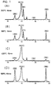
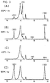
- Figs. 1 to 4 are X-ray diffraction patterns obtained with PZT thin films and the PLZT thin films in accordance with the present invention.
- PZT thin film or PLZT thin film is formed on a platinum substrate with its crystal orientation in the [111] axis.
- the substrate should be electrically conductive so that it can be used as the bottom side electrode; in addition, it should not react with PZT thin film or PLZT thin film. Because of these requirements, platinum is a very desirable material.
- the platinum substrate may be in the form of plate or thin film formed on another substrate. Incidentally, a platinum film formed on a thermally oxidized silicon wafer is oriented in the [111] axis.
- the method of the present invention consists of applying a precursor solution of PZT thin film or PLZT thin film, which is a sol of compound organometallic compound as a precursor, onto a platinum substrate oriented in the [111] direction, heat-treating the thus formed film at 150 - 550 °C for pyrolysis, and subsequently firing at 600 - 800 °C for crystallization.
- the temperature for the first heat treatment should be properly adjusted within a range of from 150 °C to 550 °C so as to control the crystal orientation of the PZT thin film or PLZT thin film.
- the firing for crystallization should be carried out within a range of from 550 °C to 800 °C. Heat treatment at above 800 °C causes PZT thin film to react with platinum, resulting in deteriorated physical properties.
- Heat treatment temperature Preferential orientation 150 - 250 °C (111) 250 - 250 °C (111) and (100) 450 - 550 °C (100) and (200)
- Fig. 1A indicates that the PZT thin film has preferential crystal orientation in the (111) plane.
- Fig. 1B indicates that the PZT thin film has preferential crystal orientation in the (111) plane and (100) plane.
- Fig. 1C indicates that the PZT thin film has no preferential crystal orientation in particular planes.
- Fig. 1D indicates that the PZT thin film has preferential crystal orientation in the (100) plane and (200) plane.
- Example 2 The same procedure as in Example 1 was repeated except that the heat treatment was carried out for 1 hour.
- the resulting samples of PZT thin film gave X-ray diffraction patterns as shown in Fig. 2 (A: 200 °C, B: 300 °C, C: 400 °C, D: 500 °C). This result is similar to that in Example 1.
- Example 2 The same procedure as in Example 2 was repeated except that the precursor solution was reflexed for 10 hours before use.
- the resulting samples of PZT thin film gave X-ray diffraction patterns as shown in Fig. 3.
- Example 2 The procedures of Example 1 were repeated using 7.2g of Pb(CH3COO)2 ⁇ 3H2O, 0.34g of La(CH3COO)3 ⁇ 1.5H2O, 3.94g of Zr(OBu)4, 2.70g of Ti(OiPr) and 55g 2-ethoxyethanol.
- the resulting PLZT was Pb 0.95 La 0.05 Zr 0.51 Ti 0.47 O3.
- the X-ray diffraction patterns are shown in Fig. 4 (A: 200 °C, B: 300 °C, C: 400 °C and D: 500 °C). Generally, they show characters similar to Fig. 1-3, but preferentiality is improved.
Landscapes
- Chemical & Material Sciences (AREA)
- Dispersion Chemistry (AREA)
- Engineering & Computer Science (AREA)
- Manufacturing & Machinery (AREA)
- Inorganic Compounds Of Heavy Metals (AREA)
- Semiconductor Memories (AREA)
- Chemically Coating (AREA)
- Inorganic Insulating Materials (AREA)
Applications Claiming Priority (2)
| Application Number | Priority Date | Filing Date | Title |
|---|---|---|---|
| JP3040592A JPH04259380A (ja) | 1991-02-13 | 1991-02-13 | Pzt強誘電体薄膜の結晶配向性制御方法 |
| JP40592/91 | 1991-02-13 |
Publications (3)
| Publication Number | Publication Date |
|---|---|
| EP0513478A2 true EP0513478A2 (de) | 1992-11-19 |
| EP0513478A3 EP0513478A3 (en) | 1993-10-06 |
| EP0513478B1 EP0513478B1 (de) | 1998-09-09 |
Family
ID=12584782
Family Applications (1)
| Application Number | Title | Priority Date | Filing Date |
|---|---|---|---|
| EP92102437A Expired - Lifetime EP0513478B1 (de) | 1991-02-13 | 1992-02-13 | Verfahren zum Kontrollieren der kristallinen Richtung einer ferroelektrischer Dünnschicht |
Country Status (5)
| Country | Link |
|---|---|
| US (1) | US5453294A (de) |
| EP (1) | EP0513478B1 (de) |
| JP (1) | JPH04259380A (de) |
| KR (1) | KR970006997B1 (de) |
| DE (1) | DE69226898T2 (de) |
Cited By (4)
| Publication number | Priority date | Publication date | Assignee | Title |
|---|---|---|---|---|
| EP0952000A3 (de) * | 1998-04-24 | 2000-04-19 | Seiko Epson Corporation | Piezoelektrisches Gerät, Tintenstrahlaufzeichnungskopf und Verfahren zur Herstellung dieses Gerätes und dieses Kopfes |
| WO2001067465A3 (en) * | 2000-03-04 | 2002-02-28 | Energenius Inc | Lead zirconate titanate dielectric thin film composites on metallic foils |
| US7042141B2 (en) * | 2003-03-26 | 2006-05-09 | The Circle For The Promotion Of Science And Engineering | Method of producing lead zirconate titanate-based thin film, dielectric device and dielectric thin film |
| JP2014175550A (ja) * | 2013-03-11 | 2014-09-22 | Ricoh Co Ltd | 圧電膜及びその製造方法 |
Families Citing this family (23)
| Publication number | Priority date | Publication date | Assignee | Title |
|---|---|---|---|---|
| JP3966479B2 (ja) * | 1993-04-16 | 2007-08-29 | 日本テキサス・インスツルメンツ株式会社 | ゾルーゲル法による強誘電体膜の形成方法及びキャパシタの製造方法 |
| US5825121A (en) * | 1994-07-08 | 1998-10-20 | Seiko Epson Corporation | Thin film piezoelectric device and ink jet recording head comprising the same |
| EP0727832B1 (de) * | 1995-02-20 | 2001-11-28 | Seiko Epson Corporation | Verfahren zur Herstellung einer piezoelektrischen Dünnschicht |
| US6025205A (en) * | 1997-01-07 | 2000-02-15 | Tong Yang Cement Corporation | Apparatus and methods of forming preferred orientation-controlled platinum films using nitrogen |
| US6054331A (en) * | 1997-01-15 | 2000-04-25 | Tong Yang Cement Corporation | Apparatus and methods of depositing a platinum film with anti-oxidizing function over a substrate |
| US6498097B1 (en) | 1997-05-06 | 2002-12-24 | Tong Yang Cement Corporation | Apparatus and method of forming preferred orientation-controlled platinum film using oxygen |
| JP3594787B2 (ja) * | 1998-02-03 | 2004-12-02 | 富士通株式会社 | 半導体装置及びその製造方法 |
| JP2000034575A (ja) | 1998-03-30 | 2000-02-02 | Minolta Co Ltd | 金属酸化物薄膜およびアレイ状金属酸化物機能性素子の製造法 |
| JP3379479B2 (ja) * | 1998-07-01 | 2003-02-24 | セイコーエプソン株式会社 | 機能性薄膜、圧電体素子、インクジェット式記録ヘッド、プリンタ、圧電体素子の製造方法およびインクジェット式記録ヘッドの製造方法、 |
| US6367132B2 (en) * | 1998-08-31 | 2002-04-09 | Eastman Kodak Company | Method of making a print head |
| GB2345379B (en) * | 1998-12-30 | 2000-12-06 | Samsung Electro Mech | Method for fabricating piezoelectric/electrostrictive thick film using seeding layer |
| US6494567B2 (en) * | 2000-03-24 | 2002-12-17 | Seiko Epson Corporation | Piezoelectric element and manufacturing method and manufacturing device thereof |
| US6541137B1 (en) * | 2000-07-31 | 2003-04-01 | Motorola, Inc. | Multi-layer conductor-dielectric oxide structure |
| US20040175585A1 (en) * | 2003-03-05 | 2004-09-09 | Qin Zou | Barium strontium titanate containing multilayer structures on metal foils |
| JP4192794B2 (ja) * | 2004-01-26 | 2008-12-10 | セイコーエプソン株式会社 | 圧電素子、圧電アクチュエーター、インクジェット式記録ヘッド、インクジェットプリンター、表面弾性波素子、周波数フィルタ、発振器、電子回路、薄膜圧電共振器、及び電子機器 |
| JP4793568B2 (ja) * | 2005-07-08 | 2011-10-12 | セイコーエプソン株式会社 | アクチュエータ装置、液体噴射ヘッド及び液体噴射装置 |
| JP2007207791A (ja) * | 2006-01-31 | 2007-08-16 | Fujitsu Ltd | 半導体装置の製造方法 |
| US8592767B2 (en) * | 2006-08-07 | 2013-11-26 | The Trustees Of The University Of Pennsylvania | Tunable ferroelectric supported catalysts and method and uses thereof |
| JP5891490B2 (ja) * | 2012-01-27 | 2016-03-23 | 株式会社ユーテック | 強誘電体膜の製造方法 |
| JP5919956B2 (ja) * | 2012-03-30 | 2016-05-18 | 三菱マテリアル株式会社 | Pzt系強誘電体薄膜の製造方法 |
| US20170092841A1 (en) * | 2015-09-29 | 2017-03-30 | Canon Kabushiki Kaisha | Substrate for piezoelectric body formation, method for manufacturing the same, piezoelectric substrate, and liquid ejection head |
| MX2018011197A (es) * | 2016-03-16 | 2019-05-16 | Xaar Technology Ltd | Un elemento de pelicula delgada piezoelectrica. |
| JP2021012942A (ja) * | 2019-07-05 | 2021-02-04 | 本多電子株式会社 | 超音波振動子及びその製造方法 |
Family Cites Families (5)
| Publication number | Priority date | Publication date | Assignee | Title |
|---|---|---|---|---|
| US4946710A (en) * | 1987-06-02 | 1990-08-07 | National Semiconductor Corporation | Method for preparing PLZT, PZT and PLT sol-gels and fabricating ferroelectric thin films |
| GB8809608D0 (en) * | 1988-04-22 | 1988-05-25 | Alcan Int Ltd | Sol-gel method of making ceramics |
| US4963390A (en) * | 1988-10-05 | 1990-10-16 | The Aerospace Corporation | Metallo-organic solution deposition (MOSD) of transparent, crystalline ferroelectric films |
| KR920701048A (ko) * | 1989-04-21 | 1992-08-11 | 원본미기재 | 졸 겔 가공에 의한 박막 세라믹 제법 |
| WO1990013149A1 (en) * | 1989-04-27 | 1990-11-01 | Queen's University At Kingston | SOL GEL PROCESS FOR PREPARING Pb(Zr,Ti)O3 THIN FILMS |
-
1991
- 1991-02-13 JP JP3040592A patent/JPH04259380A/ja active Pending
-
1992
- 1992-02-13 KR KR1019920002091A patent/KR970006997B1/ko not_active Expired - Fee Related
- 1992-02-13 DE DE69226898T patent/DE69226898T2/de not_active Expired - Fee Related
- 1992-02-13 EP EP92102437A patent/EP0513478B1/de not_active Expired - Lifetime
-
1993
- 1993-04-16 US US08/049,634 patent/US5453294A/en not_active Expired - Lifetime
Cited By (6)
| Publication number | Priority date | Publication date | Assignee | Title |
|---|---|---|---|---|
| EP0952000A3 (de) * | 1998-04-24 | 2000-04-19 | Seiko Epson Corporation | Piezoelektrisches Gerät, Tintenstrahlaufzeichnungskopf und Verfahren zur Herstellung dieses Gerätes und dieses Kopfes |
| US6411017B1 (en) | 1998-04-24 | 2002-06-25 | Seiko Epson Corporation | Piezoelectric device, ink jet recording head, and methods of manufacturing said device and head |
| WO2001067465A3 (en) * | 2000-03-04 | 2002-02-28 | Energenius Inc | Lead zirconate titanate dielectric thin film composites on metallic foils |
| US6623865B1 (en) | 2000-03-04 | 2003-09-23 | Energenius, Inc. | Lead zirconate titanate dielectric thin film composites on metallic foils |
| US7042141B2 (en) * | 2003-03-26 | 2006-05-09 | The Circle For The Promotion Of Science And Engineering | Method of producing lead zirconate titanate-based thin film, dielectric device and dielectric thin film |
| JP2014175550A (ja) * | 2013-03-11 | 2014-09-22 | Ricoh Co Ltd | 圧電膜及びその製造方法 |
Also Published As
| Publication number | Publication date |
|---|---|
| JPH04259380A (ja) | 1992-09-14 |
| EP0513478B1 (de) | 1998-09-09 |
| DE69226898T2 (de) | 1999-03-04 |
| EP0513478A3 (en) | 1993-10-06 |
| KR970006997B1 (ko) | 1997-05-01 |
| US5453294A (en) | 1995-09-26 |
| DE69226898D1 (de) | 1998-10-15 |
Similar Documents
| Publication | Publication Date | Title |
|---|---|---|
| EP0513478A2 (de) | Verfahren zum Kontrollieren der kristallinen Richtung einer ferroelektrischer Dünnschicht | |
| JP3021930B2 (ja) | 強誘電体薄膜の結晶配向性制御方法 | |
| US5811181A (en) | Ferroelectric thin film, ferroelectric thin film covering substrate and manufacturing method of ferroelectric thin film | |
| JP3341357B2 (ja) | 圧電体薄膜素子 | |
| US5188902A (en) | Production of PT/PZT/PLZI thin films, powders, and laser `direct write` patterns | |
| JPWO2009157189A1 (ja) | 圧電体素子とその製造方法 | |
| US8557352B2 (en) | Method of making a metal oxide film, laminates and electronic devices | |
| JP2532381B2 (ja) | 強誘電体薄膜素子及びその製造方法 | |
| US6528863B1 (en) | Perovskite-containing composite material, method of manufacturing said material, electronic component and module | |
| JP2995290B2 (ja) | Pzt系強誘電体薄膜の形成方法 | |
| JP4122430B2 (ja) | 強誘電体膜 | |
| JP3105081B2 (ja) | 強誘電体薄膜の製造方法 | |
| JP3105080B2 (ja) | 強誘電体薄膜の製造方法 | |
| JP3363091B2 (ja) | 誘電体メモリの製造方法 | |
| Aegerter | Ferroelectric thin coatings | |
| JP3436554B2 (ja) | 複合酸化物薄膜及びその製造法 | |
| JPH0762235B2 (ja) | 強誘電体薄膜の製造方法 | |
| JPH05254994A (ja) | 強誘電性薄膜 | |
| JPH05298920A (ja) | 高誘電体薄膜 | |
| JPH07187894A (ja) | 強誘電性薄膜 | |
| JP3379796B2 (ja) | 強誘電体薄膜製造方法 | |
| JPH065947A (ja) | 強誘電体薄膜の製造方法 | |
| JPH10291887A (ja) | セラミックス薄膜の製造方法 | |
| JP3268649B2 (ja) | (Pb,La)(ZrxTiy)O3の配向膜を有する複合結晶体の製法 | |
| JP2006076835A (ja) | 強誘電体薄膜及びその製造方法 |
Legal Events
| Date | Code | Title | Description |
|---|---|---|---|
| PUAI | Public reference made under article 153(3) epc to a published international application that has entered the european phase |
Free format text: ORIGINAL CODE: 0009012 |
|
| AK | Designated contracting states |
Kind code of ref document: A2 Designated state(s): DE FR GB |
|
| PUAL | Search report despatched |
Free format text: ORIGINAL CODE: 0009013 |
|
| AK | Designated contracting states |
Kind code of ref document: A3 Designated state(s): DE FR GB |
|
| 17P | Request for examination filed |
Effective date: 19931208 |
|
| 17Q | First examination report despatched |
Effective date: 19950125 |
|
| GRAG | Despatch of communication of intention to grant |
Free format text: ORIGINAL CODE: EPIDOS AGRA |
|
| GRAG | Despatch of communication of intention to grant |
Free format text: ORIGINAL CODE: EPIDOS AGRA |
|
| GRAH | Despatch of communication of intention to grant a patent |
Free format text: ORIGINAL CODE: EPIDOS IGRA |
|
| GRAH | Despatch of communication of intention to grant a patent |
Free format text: ORIGINAL CODE: EPIDOS IGRA |
|
| GRAA | (expected) grant |
Free format text: ORIGINAL CODE: 0009210 |
|
| AK | Designated contracting states |
Kind code of ref document: B1 Designated state(s): DE FR GB |
|
| REF | Corresponds to: |
Ref document number: 69226898 Country of ref document: DE Date of ref document: 19981015 |
|
| ET | Fr: translation filed | ||
| PGFP | Annual fee paid to national office [announced via postgrant information from national office to epo] |
Ref country code: FR Payment date: 19990126 Year of fee payment: 8 |
|
| PGFP | Annual fee paid to national office [announced via postgrant information from national office to epo] |
Ref country code: GB Payment date: 19990211 Year of fee payment: 8 |
|
| PGFP | Annual fee paid to national office [announced via postgrant information from national office to epo] |
Ref country code: DE Payment date: 19990331 Year of fee payment: 8 |
|
| PLBE | No opposition filed within time limit |
Free format text: ORIGINAL CODE: 0009261 |
|
| STAA | Information on the status of an ep patent application or granted ep patent |
Free format text: STATUS: NO OPPOSITION FILED WITHIN TIME LIMIT |
|
| 26N | No opposition filed | ||
| PG25 | Lapsed in a contracting state [announced via postgrant information from national office to epo] |
Ref country code: GB Free format text: LAPSE BECAUSE OF NON-PAYMENT OF DUE FEES Effective date: 20000213 |
|
| GBPC | Gb: european patent ceased through non-payment of renewal fee |
Effective date: 20000213 |
|
| PG25 | Lapsed in a contracting state [announced via postgrant information from national office to epo] |
Ref country code: FR Free format text: LAPSE BECAUSE OF NON-PAYMENT OF DUE FEES Effective date: 20001031 |
|
| PG25 | Lapsed in a contracting state [announced via postgrant information from national office to epo] |
Ref country code: DE Free format text: LAPSE BECAUSE OF NON-PAYMENT OF DUE FEES Effective date: 20001201 |
|
| REG | Reference to a national code |
Ref country code: FR Ref legal event code: ST |