EP0514018A2 - Verfahren zum Herstellen einer mit niedriger Fehlerdichte Halbleiter-Heterostruktur und sich daraus ergebenden Anordnungen - Google Patents
Verfahren zum Herstellen einer mit niedriger Fehlerdichte Halbleiter-Heterostruktur und sich daraus ergebenden Anordnungen Download PDFInfo
- Publication number
- EP0514018A2 EP0514018A2 EP92303475A EP92303475A EP0514018A2 EP 0514018 A2 EP0514018 A2 EP 0514018A2 EP 92303475 A EP92303475 A EP 92303475A EP 92303475 A EP92303475 A EP 92303475A EP 0514018 A2 EP0514018 A2 EP 0514018A2
- Authority
- EP
- European Patent Office
- Prior art keywords
- layer
- silicon
- germanium
- alloy
- graded
- Prior art date
- Legal status (The legal status is an assumption and is not a legal conclusion. Google has not performed a legal analysis and makes no representation as to the accuracy of the status listed.)
- Withdrawn
Links
Images

Classifications
-
- H—ELECTRICITY
- H10—SEMICONDUCTOR DEVICES; ELECTRIC SOLID-STATE DEVICES NOT OTHERWISE PROVIDED FOR
- H10H—INORGANIC LIGHT-EMITTING SEMICONDUCTOR DEVICES HAVING POTENTIAL BARRIERS
- H10H20/00—Individual inorganic light-emitting semiconductor devices having potential barriers, e.g. light-emitting diodes [LED]
- H10H20/01—Manufacture or treatment
- H10H20/011—Manufacture or treatment of bodies, e.g. forming semiconductor layers
- H10H20/013—Manufacture or treatment of bodies, e.g. forming semiconductor layers having light-emitting regions comprising only Group III-V materials
- H10H20/0133—Manufacture or treatment of bodies, e.g. forming semiconductor layers having light-emitting regions comprising only Group III-V materials with a substrate not being Group III-V materials
-
- H—ELECTRICITY
- H10—SEMICONDUCTOR DEVICES; ELECTRIC SOLID-STATE DEVICES NOT OTHERWISE PROVIDED FOR
- H10D—INORGANIC ELECTRIC SEMICONDUCTOR DEVICES
- H10D30/00—Field-effect transistors [FET]
- H10D30/01—Manufacture or treatment
- H10D30/015—Manufacture or treatment of FETs having heterojunction interface channels or heterojunction gate electrodes, e.g. HEMT
-
- H—ELECTRICITY
- H10—SEMICONDUCTOR DEVICES; ELECTRIC SOLID-STATE DEVICES NOT OTHERWISE PROVIDED FOR
- H10D—INORGANIC ELECTRIC SEMICONDUCTOR DEVICES
- H10D84/00—Integrated devices formed in or on semiconductor substrates that comprise only semiconducting layers, e.g. on Si wafers or on GaAs-on-Si wafers
- H10D84/01—Manufacture or treatment
- H10D84/02—Manufacture or treatment characterised by using material-based technologies
- H10D84/08—Manufacture or treatment characterised by using material-based technologies using combinations of technologies, e.g. using both Si and SiC technologies or using both Si and Group III-V technologies
-
- H—ELECTRICITY
- H10—SEMICONDUCTOR DEVICES; ELECTRIC SOLID-STATE DEVICES NOT OTHERWISE PROVIDED FOR
- H10H—INORGANIC LIGHT-EMITTING SEMICONDUCTOR DEVICES HAVING POTENTIAL BARRIERS
- H10H29/00—Integrated devices, or assemblies of multiple devices, comprising at least one light-emitting semiconductor element covered by group H10H20/00
- H10H29/10—Integrated devices comprising at least one light-emitting semiconductor component covered by group H10H20/00
-
- H—ELECTRICITY
- H10—SEMICONDUCTOR DEVICES; ELECTRIC SOLID-STATE DEVICES NOT OTHERWISE PROVIDED FOR
- H10P—GENERIC PROCESSES OR APPARATUS FOR THE MANUFACTURE OR TREATMENT OF DEVICES COVERED BY CLASS H10
- H10P14/00—Formation of materials, e.g. in the shape of layers or pillars
- H10P14/20—Formation of materials, e.g. in the shape of layers or pillars of semiconductor materials
- H10P14/22—Formation of materials, e.g. in the shape of layers or pillars of semiconductor materials using physical deposition, e.g. vacuum deposition or sputtering
-
- H—ELECTRICITY
- H10—SEMICONDUCTOR DEVICES; ELECTRIC SOLID-STATE DEVICES NOT OTHERWISE PROVIDED FOR
- H10P—GENERIC PROCESSES OR APPARATUS FOR THE MANUFACTURE OR TREATMENT OF DEVICES COVERED BY CLASS H10
- H10P14/00—Formation of materials, e.g. in the shape of layers or pillars
- H10P14/20—Formation of materials, e.g. in the shape of layers or pillars of semiconductor materials
- H10P14/24—Formation of materials, e.g. in the shape of layers or pillars of semiconductor materials using chemical vapour deposition [CVD]
-
- H—ELECTRICITY
- H10—SEMICONDUCTOR DEVICES; ELECTRIC SOLID-STATE DEVICES NOT OTHERWISE PROVIDED FOR
- H10P—GENERIC PROCESSES OR APPARATUS FOR THE MANUFACTURE OR TREATMENT OF DEVICES COVERED BY CLASS H10
- H10P14/00—Formation of materials, e.g. in the shape of layers or pillars
- H10P14/20—Formation of materials, e.g. in the shape of layers or pillars of semiconductor materials
- H10P14/29—Formation of materials, e.g. in the shape of layers or pillars of semiconductor materials characterised by the substrates
- H10P14/2901—Materials
- H10P14/2902—Materials being Group IVA materials
- H10P14/2905—Silicon, silicon germanium or germanium
-
- H—ELECTRICITY
- H10—SEMICONDUCTOR DEVICES; ELECTRIC SOLID-STATE DEVICES NOT OTHERWISE PROVIDED FOR
- H10P—GENERIC PROCESSES OR APPARATUS FOR THE MANUFACTURE OR TREATMENT OF DEVICES COVERED BY CLASS H10
- H10P14/00—Formation of materials, e.g. in the shape of layers or pillars
- H10P14/20—Formation of materials, e.g. in the shape of layers or pillars of semiconductor materials
- H10P14/32—Formation of materials, e.g. in the shape of layers or pillars of semiconductor materials characterised by intermediate layers between substrates and deposited layers
- H10P14/3202—Materials thereof
- H10P14/3204—Materials thereof being Group IVA semiconducting materials
- H10P14/3211—Silicon, silicon germanium or germanium
-
- H—ELECTRICITY
- H10—SEMICONDUCTOR DEVICES; ELECTRIC SOLID-STATE DEVICES NOT OTHERWISE PROVIDED FOR
- H10P—GENERIC PROCESSES OR APPARATUS FOR THE MANUFACTURE OR TREATMENT OF DEVICES COVERED BY CLASS H10
- H10P14/00—Formation of materials, e.g. in the shape of layers or pillars
- H10P14/20—Formation of materials, e.g. in the shape of layers or pillars of semiconductor materials
- H10P14/32—Formation of materials, e.g. in the shape of layers or pillars of semiconductor materials characterised by intermediate layers between substrates and deposited layers
- H10P14/3242—Structure
- H10P14/3244—Layer structure
- H10P14/3254—Graded layers
-
- H—ELECTRICITY
- H10—SEMICONDUCTOR DEVICES; ELECTRIC SOLID-STATE DEVICES NOT OTHERWISE PROVIDED FOR
- H10P—GENERIC PROCESSES OR APPARATUS FOR THE MANUFACTURE OR TREATMENT OF DEVICES COVERED BY CLASS H10
- H10P14/00—Formation of materials, e.g. in the shape of layers or pillars
- H10P14/20—Formation of materials, e.g. in the shape of layers or pillars of semiconductor materials
- H10P14/34—Deposited materials, e.g. layers
- H10P14/3402—Deposited materials, e.g. layers characterised by the chemical composition
- H10P14/3414—Deposited materials, e.g. layers characterised by the chemical composition being group IIIA-VIA materials
- H10P14/3418—Phosphides
-
- H—ELECTRICITY
- H10—SEMICONDUCTOR DEVICES; ELECTRIC SOLID-STATE DEVICES NOT OTHERWISE PROVIDED FOR
- H10P—GENERIC PROCESSES OR APPARATUS FOR THE MANUFACTURE OR TREATMENT OF DEVICES COVERED BY CLASS H10
- H10P14/00—Formation of materials, e.g. in the shape of layers or pillars
- H10P14/20—Formation of materials, e.g. in the shape of layers or pillars of semiconductor materials
- H10P14/34—Deposited materials, e.g. layers
- H10P14/3402—Deposited materials, e.g. layers characterised by the chemical composition
- H10P14/3414—Deposited materials, e.g. layers characterised by the chemical composition being group IIIA-VIA materials
- H10P14/3421—Arsenides
-
- H—ELECTRICITY
- H10—SEMICONDUCTOR DEVICES; ELECTRIC SOLID-STATE DEVICES NOT OTHERWISE PROVIDED FOR
- H10D—INORGANIC ELECTRIC SEMICONDUCTOR DEVICES
- H10D62/00—Semiconductor bodies, or regions thereof, of devices having potential barriers
- H10D62/80—Semiconductor bodies, or regions thereof, of devices having potential barriers characterised by the materials
- H10D62/82—Heterojunctions
- H10D62/822—Heterojunctions comprising only Group IV materials heterojunctions, e.g. Si/Ge heterojunctions
-
- H—ELECTRICITY
- H10—SEMICONDUCTOR DEVICES; ELECTRIC SOLID-STATE DEVICES NOT OTHERWISE PROVIDED FOR
- H10H—INORGANIC LIGHT-EMITTING SEMICONDUCTOR DEVICES HAVING POTENTIAL BARRIERS
- H10H20/00—Individual inorganic light-emitting semiconductor devices having potential barriers, e.g. light-emitting diodes [LED]
- H10H20/80—Constructional details
- H10H20/83—Electrodes
- H10H20/831—Electrodes characterised by their shape
- H10H20/8314—Electrodes characterised by their shape extending at least partially onto an outer side surface of the bodies
-
- Y—GENERAL TAGGING OF NEW TECHNOLOGICAL DEVELOPMENTS; GENERAL TAGGING OF CROSS-SECTIONAL TECHNOLOGIES SPANNING OVER SEVERAL SECTIONS OF THE IPC; TECHNICAL SUBJECTS COVERED BY FORMER USPC CROSS-REFERENCE ART COLLECTIONS [XRACs] AND DIGESTS
- Y10—TECHNICAL SUBJECTS COVERED BY FORMER USPC
- Y10S—TECHNICAL SUBJECTS COVERED BY FORMER USPC CROSS-REFERENCE ART COLLECTIONS [XRACs] AND DIGESTS
- Y10S438/00—Semiconductor device manufacturing: process
- Y10S438/938—Lattice strain control or utilization
Definitions
- This invention relates to a method for making a semiconductor heterostructure of germanium-silicon alloy that has low threading dislocation density in the alloy layer and to devices made thereby.
- Such low defect structures are particularly useful as buffer layers for making semiconductor devices comprising indium gallium phosphide, gallium arsenide or strained layers of silicon.
- germanium-silicon alloy Ge x Si 1-x grown on silicon substrates would permit a variety of optoelectronic devices, such as LEDs, marrying the electronic processing technology of silicon VLSI circuits with the optical component technology available in direct band semiconductors.
- an intermediate epitaxial layer of germanium-silicon alloy would permit the epitaxial deposition of gallium arsenide overlying a silicon substrate and thus permit a variety of new optoelectronic devices using silicon electronic components and gallium arsenide optical components.
- their practical utility has been limited by high defect densities in heterostructure layers grown on silicon substrates.
- Dislocation defects partition an otherwise monolithic crystal structure and introduce unwanted and abrupt changes in electrical and optical properties. Dislocation defects arise in efforts to epitaxially grow one kind of crystalline material on a substrate of a different kind of material due to different crystal lattice sizes of the two materials. Dislocations form at the mismatched interface to relieve the misfit strain. Many of the misfit dislocations have vertical components, termed threading segments, which extend at a slant angle through any subsequent layers. Such threading defects in the active regions of semiconductor devices seriously degrade device performance.
- a variety of approaches have been used to reduce dislocations with varying degrees of success.
- One approach is to limit the heterolayer to a thin layer of material that has a lattice crystal structure closely matching the substrate. Typically the lattice mismatch is within 1% and thickness of the layer is kept below a critical thickness for defect formation.
- the substrate acts as a template for growth of the heterolayer which elastically conforms to the substrate template. While this approach eliminates dislocations in a number of structures, there are relatively few near lattice-matched systems with large energy band offsets. Thus with this approach the design options for new devices are limited.
- This approach permits the fabrication of a variety of devices and circuits which can be made on limited area surfaces having an area of less than about 10,000 square micrometers
- a third approach is to deposit successive layers of germanium-silicon alloy on a silicon substrate, increasing the germanium content with each successive layer.
- the goal is to avoid dislocations by spreading the strain among successive layers.
- this approach has not worked. For example, it has been found that step grading 20% Ge over 2000 angstroms to produce pure Ge results in substantially the same high dislocation density as depositing pure Ge on Si. See J. M. Baribeau et al., 63 Journal of Applied Physics 5738 (1988). Applicants believe that this approach fails because at conventional growth temperatures --typically about 550° C-- the initial layer of Si-Ge is almost entirely elastically strained.
- FIG. 1 is a flow diagram illustrating the process for making a low defect density semiconductor heterostructure in accordance with the invention.
- the first step is providing a silicon substrate.
- the substrate is a standard (100) oriented silicon wafer of the type typically used in the fabrication of integrated circuits.
- the substrate is provided with one or more large area recessed tubs by conventional photolithographic patterning and etching.
- the tubs can have an area in excess of 12,000 square micrometers and a depth of several micrometers, depending upon the thickness of germanium-silicon alloy to be grown.
- the objective is to provide a tub of proper depth so that a germanium-silicon alloy layer grown in the tub will be substantially coplanar with the non-recessed portion of the silicon substrate.
- the second step of the process is to grow at high temperature on the silicon substrate a large area, graded layer of germanium-silicon alloy, Ge x Si 1-x .
- the growth process is preferably chemical vapor deposition (CVD) or molecular beam epitaxy (MBE).
- the substrate growth starting temperature should be in the range 850° C - 1100° C, and the area of the graded alloy can exceed 12,000 square micrometers.
- the starting composition is preferably pure silicon.
- Germanium is introduced to form Ge x Si 1-x at a gradient of less than about 25% per micron.
- the grading is linear at a rate of about 10% per micron.
- the grading can be stepwise at similar gradients.
- the germanium content of the alloy increases, the growth temperature is advantageously scaled down in proportion to the reduced melting temperature of the alloy. The objective is to avoid melting the alloy.
- Graded growth of Ge x Si 1-x is continued until a desired final composition is reached.
- the choice of final composition depends upon the intended use of the heterostructure. If, for example, the structure is to be used as a substrate for growing a strained layer silicon device, the final Ge concentration should fall within the range of 10-50%. If the structure is to be used as a substrate for an indium gallium phosphide device, the final Ge concentration should fall within the range of 65-100%. On the other hand, if the structure is to be used as a substrate for GaAs or GaAs/AlGaAs devices, the Ge concentration is preferably about 100%.
- an optional cap layer with the same final composition can be grown on the graded layer to a thickness in excess of 100 angstroms and preferably in excess of one micrometer. The effect of the cap layer is to further relax the low level of residual strain at the top of the graded layer.
- Example 1 Heterostructure Substrate (MBE)
- a (100) oriented silicon substrate is provided with a large area rectangular tub approximately ten micrometers deep by covering the major surface with a masking layer of silicon oxide, etching a rectangular opening in the oxide mask to define the periphery of the tub, and then etching the exposed silicon with ethylene-diamine-pyrocatechol (EDP).
- EDP ethylene-diamine-pyrocatechol
- the EDP etch produces smooth tub surfaces with sidewalls in the (111) planes of the silicon substrate.
- the substrate is then cleaned with a 3:1 mixture of H2SO4 and H2O2 for ten minutes and with buffered HF for 1 minute.
- the cleaned substrate is placed in a Riber EVA 32 Silicon MBE Apparatus controlled by a Sentinel 3 Deposition Rate Controller.
- the chamber is evacuated to a pressure of less than 10 ⁇ 9 Torr, and any oxide on the tub surfaces is dissociated by heating the substrate to about 800° C and applying a low flux silicon beam at a rate of about 0.05 angstrom/s. Silicon growth at higher rate is continued to a thickness of about 0.1 micrometer to form a silicon buffer layer.
- the substrate temperature is increased to about 900° C and the graded layer is grown.
- Graded growth is begun with pure silicon at a rate of about 3 angstroms per second. The total growth rate is kept constant while introducing germanium at a linear gradient of about 10% per micrometer. The objective is to keep growth near thermal equilibrium.
- the parameter variations for graded growth to 100% germanium at 10% per micrometer grading are set forth in the Table 1, giving thickness, percent of Germanium, temperature and current rates at various times into growth. After 100% germanium is reached, a final germanium cap layer having a thickness in the range between 1000 angstroms and one micrometer is grown on top.
- Structures with less than 100% germanium can be obtained by terminating graded growth at the desired germanium concentration and growing the final cap layer at that concentration.
- a 100 mm (100) Si wafer was cleaned in dilute HF (1% in H2O) and spin-dried in N2.
- the wafer was loaded into an RTCVD reactor and pumped down to a base pressure of 10 ⁇ 7 Torr.
- the wafer was heated to 1000° C for 15 seconds in flowing H2 (3 lpm) to remove residual oxygen and carbon, and then cooled in 2 seconds to 900° C.
- deposition was commenced by depositing a Si buffer approximately 1000 ⁇ thick. This was accomplished using SiH2Cl2 (1% in H2, 1 lpm) for 1 minute at a pressure of about 4 Torr. Immediately thereafter, GeH4 (1% GeH4 in H2) was introduced gradually to create a Si-Ge alloy layer that increased from 0 to 50% Ge. The GeH4 flow can be increased by 4 sccm flow increments every 40 seconds. The SiH2Cl2 was decreased by the same flow increment in the same time scale; thus, the total GeH4 and SiH2Cl2 flow was maintained at 1 lpm. Deposition at 900° C resulted in a Si-Ge graded alloy layer that continually relaxed as it was grown.
- Heterostructures fabricated as described in Examples 1 and 2 demonstrate a reduction in defects as compared with conventionally fabricated heterostructures.
- Triple crystal X-ray diffraction shows that for 0. 10 ⁇ x ⁇ 0.50, the layers are totally relaxed.
- the Ge x Si 1-x cap layers, when examined by plan-view and cross-sectional transmission electron microscopy are threading dislocation free.
- Photoluminescence spectra from the cap layers are substantially identical to photoluminescence from bulk Ge x Si 1-x .
- These low defect heterostructures can serve as buffer layers for epitaxially growing a wide variety of devices varying from those employing strained layer of silicon to those employing III-V semiconductors.
- FIG. 2 is a schematic cross section of a device employing a low defect heterostructure to produce a strained silicon MODFET.
- the MODFET is fabricated on a heterostructure comprising a Ge x Si 1-x cap layer 1 grown on a graded layer 2, all disposed on a silicon substrate 3.
- the MODFET fabricated on the heterolayer comprises, in essence, a strained layer of silicon 4 epitaxially grown on layer 1.
- Another layer 5 of Ge x Si 1-x (initially intrinsic but n-doped after 50 to 900 angstroms) is grown over the silicon and, n+ spaced apart contact regions 6A and 6B are formed to contact the strained silicon layer 4.
- Ohmic contacts 8A and 8B are made with the n+ contact regions 6A and 6B, and a Schottky barrier contact 7 to layer 5 is disposed between the spaced apart ohmic contacts.
- a dielectric layer 9 advantageously separates the contacts 7, 8A, and 8B.
- Silicon layer 4 preferably has a thickness in the range 100 angstroms to 1000 angstroms and is preferably undoped.
- Ge x Si 1-x layer 5 preferably has a thickness in the range 50 angstroms to 1000 angstroms.
- Layer 5 is preferably intrinsic for 50 to 900 angstoms and then n+ doped with antimony, phosphorus or arsenic to a concentration in the range 1x10¹⁷/cm3 - 5x10¹⁸/cm3.
- Layer 5 preferably has a concentration of Ge not less than that of cap layer 1.
- the n+ contact regions 6A and 6B are preferably formed by implanting antimony, arsenic or phosphorus to silicon layer 4 at a concentration of 1019/cm3.
- the ohmic contacts 8A and 8B can be layers of aluminum and the Schottky contact 7 can be a layer of platinum.
- the resulting MODFET acts as a field effect transistor with the advantage of higher speed.
- the application of a signal voltage bias to the Schottky contact 7 (commonly known as the gate) changes the electron density inside the Si layer 4, which in turn changes the sheet conductance of the channel between 8A and 8B and results in transistor action.
- the strained silicon layer is a particularly high speed path for at least three reasons: 1) the straining of the silicon alters the energy bands of the silicon to favor conduction by low effective mass, high mobility electrons, 2) the silicon layer is free of impurities to interfere with electron flow, and 3) the silicon layer grown on a low defect substrate has a low concentration of defects to interfere with electron flow.
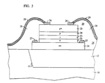
- FIG. 3 is a schematic cross section of an indium gallium arsenide surface emitting LED fabricated on a heterolayer.
- the LED 20 is fabricated on a heterostructure comprising a Ge x Si 1-x layer 12 grown within a large area tub 11 on a silicon substrate 10.
- the heterostructure is fabricated essentially as described above, except that the Ge x Si 1-x is doped with p-type impurities, such as Be, to a concentration of 1018cm ⁇ 3.
- the LED 20 is fabricated on the Ge x Si 1-x using conventional processes such as chemical beam epitaxy to form the constituent layers 21-25 whose thicknesses, constituency and doping are set forth in table 2 below:
- Ohmic contact 26 is formed to contact p-doped layer 25 by depositing a layer of gold-zinc alloy and photolithographically patterning the metal to form a annular ring.
- the portion of layers 22-25 outside the metal contact ring 26 can be etched away.
- a mesa is etched around ring 26 terminating on n-doped layer 21.
- etching is by reactive ion etching in order to obtain a mesa with vertical side walls around the periphery of ring 26.
- Next ohmic contact 27 is made with the now exposed n-doped layer 21 as by depositing a layer of gold-germanium alloy and photolithographically defining annular contact ring 27 around the mesa. For further isolation, a mesa concentric with ring 27 can be chemically etched through layer 21.
- the final steps involve depositing passivating insulating layers 28 and forming metal interconnects 29 to contacts 26 and 27 in accordance with techniques well known in the art.
- the interconnects can advantageously extend to integrated electronic circuitry (not shown) formed on the silicon substrate.
- a DC bias voltage applied between contacts 26 and 27 induces emission of light through the center of ring 26.
- a particular advantage of this embodiment is that the composition of the Ge x Si 1-x layer can be chosen to lattice match a variety of indium gallium phosphide compounds giving a wide choice of emission wavelengths. For example, when the indium gallium phosphide compound matches a Ge-Si buffer with 65-70% Ge, the emission is been whereas a compound lattice matched to 100% Ge emits red. Thus much of the visible range can be covered.
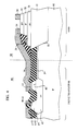
- FIG. 4 is a schematic cross section of a GaAs surface emitting LED fabricated on a heterolayer.
- the LED 30 is fabricated on a heterostructure comprising a Ge x Si 1-x layer 12 grown within a large area tub 11 on a silicon substrate 10.
- the LED is shown connected via a metal lead 36 to a drive transistor 40 integrally formed in silicon substrate 10.
- the Ge x Si 1-x layer is formed in tub 11 as described in Example 1 above.
- the Ge x Si 1-x is preferably undoped and achieves a final composition consisting essentially of pure germanium in order to lattice match the materials of LED 30.
- LED 30 comprises a layer of n-doped Al y Ga 1-y As 31 grown on the Ge surface, as by MBE, a layer of p-doped GaAs 32 grown on layer 31 and a layer 33 of p+ doped Al y Ga 1-y As grown on layer 32.
- the LED has an annular p-type ohmic contact 34 to layer 33 and an n-type ohmic contact 35 to layer 31.
- n-layer 31 can be doped with silicon to a concentration of 1018/cm3 and have a thickness of 0.5 micrometer
- p-layer 32 can be doped with Be to a concentration of 1016/cm3 and have a thickness of 0.6 micrometer
- P+ layer 32 can be doped with Be to 1019/cm3 and have a thickness of 0.5 micrometers
- the n-contact 35 can be a composite layer of nickel, titanium and gold
- the p-contact 34 can be AuBe alloy.
- the LED 30 can be connected to transistor 40 with aluminum interconnects 36.
- Drive transistor 40 consists essentially of an n-type emitter 41, a p-type base 42 and an n-turn collector 43 integrally fabricated on silicon substrate 10 in accordance with conventional techniques well known in the art.
Landscapes
- Recrystallisation Techniques (AREA)
- Physical Deposition Of Substances That Are Components Of Semiconductor Devices (AREA)
Applications Claiming Priority (2)
| Application Number | Priority Date | Filing Date | Title |
|---|---|---|---|
| US07/690,429 US5221413A (en) | 1991-04-24 | 1991-04-24 | Method for making low defect density semiconductor heterostructure and devices made thereby |
| US690429 | 1991-04-24 |
Publications (2)
| Publication Number | Publication Date |
|---|---|
| EP0514018A2 true EP0514018A2 (de) | 1992-11-19 |
| EP0514018A3 EP0514018A3 (en) | 1994-06-29 |
Family
ID=24772416
Family Applications (1)
| Application Number | Title | Priority Date | Filing Date |
|---|---|---|---|
| EP19920303475 Withdrawn EP0514018A3 (en) | 1991-04-24 | 1992-04-16 | Method for making low defect density semiconductor heterostructure and devices made thereby |
Country Status (3)
| Country | Link |
|---|---|
| US (1) | US5221413A (de) |
| EP (1) | EP0514018A3 (de) |
| JP (1) | JP2792785B2 (de) |
Cited By (57)
| Publication number | Priority date | Publication date | Assignee | Title |
|---|---|---|---|---|
| DE4438380C1 (de) * | 1994-10-27 | 1996-01-25 | Inst Halbleiterphysik Gmbh | Verfahren zur Abscheidung von einkristallinen Mischkristallschichten aus Ge¶x¶Si¶1¶¶-¶¶x¶ für Halbleiterbauelemente |
| WO1998059365A1 (en) * | 1997-06-24 | 1998-12-30 | Massachusetts Institute Of Technology | CONTROLLING THREADING DISLOCATION DENSITIES IN Ge ON Si USING GRADED GeSi LAYERS AND PLANARIZATION |
| WO1999014804A1 (en) * | 1997-09-16 | 1999-03-25 | Massachusetts Institute Of Technology | CO-PLANAR Si AND Ge COMPOSITE SUBSTRATE AND METHOD OF PRODUCING SAME |
| WO2001022482A1 (en) * | 1999-09-20 | 2001-03-29 | Amberwave Systems Corporation | Method of producing relaxed silicon germanium layers |
| US6392257B1 (en) | 2000-02-10 | 2002-05-21 | Motorola Inc. | Semiconductor structure, semiconductor device, communicating device, integrated circuit, and process for fabricating the same |
| US6410941B1 (en) | 2000-06-30 | 2002-06-25 | Motorola, Inc. | Reconfigurable systems using hybrid integrated circuits with optical ports |
| US6427066B1 (en) | 2000-06-30 | 2002-07-30 | Motorola, Inc. | Apparatus and method for effecting communications among a plurality of remote stations |
| US6462360B1 (en) | 2001-08-06 | 2002-10-08 | Motorola, Inc. | Integrated gallium arsenide communications systems |
| US6472694B1 (en) | 2001-07-23 | 2002-10-29 | Motorola, Inc. | Microprocessor structure having a compound semiconductor layer |
| US6477285B1 (en) | 2000-06-30 | 2002-11-05 | Motorola, Inc. | Integrated circuits with optical signal propagation |
| WO2002048434A3 (en) * | 2000-12-14 | 2003-01-16 | Nitronex Corp | Gallium nitride materials and methods for forming layers thereof |
| WO2002063665A3 (en) * | 2001-02-08 | 2003-01-23 | Amberwave Systems Corp | RELAXED InXGa1-xAs LAYERS INTEGRATED WITH Si |
| US6563118B2 (en) | 2000-12-08 | 2003-05-13 | Motorola, Inc. | Pyroelectric device on a monocrystalline semiconductor substrate and process for fabricating same |
| US6583034B2 (en) | 2000-11-22 | 2003-06-24 | Motorola, Inc. | Semiconductor structure including a compliant substrate having a graded monocrystalline layer and methods for fabricating the structure and semiconductor devices including the structure |
| US6589856B2 (en) | 2001-08-06 | 2003-07-08 | Motorola, Inc. | Method and apparatus for controlling anti-phase domains in semiconductor structures and devices |
| US6589335B2 (en) | 2001-02-08 | 2003-07-08 | Amberwave Systems Corporation | Relaxed InxGa1-xAs layers integrated with Si |
| US6594293B1 (en) | 2001-02-08 | 2003-07-15 | Amberwave Systems Corporation | Relaxed InxGa1-xAs layers integrated with Si |
| WO2003069657A1 (fr) * | 2002-02-15 | 2003-08-21 | Centre National De La Recherche Scientifique | Procede de formation de couche de carbure de silicium ou de nitrure d'element iii sur un substrat adapte |
| WO2003054256A3 (de) * | 2001-12-21 | 2003-10-23 | Aixtron Ag | Verfahren und vorrichtung zum abscheiden kristalliner schichten auf kristallinen substraten |
| US6638838B1 (en) | 2000-10-02 | 2003-10-28 | Motorola, Inc. | Semiconductor structure including a partially annealed layer and method of forming the same |
| US6639249B2 (en) | 2001-08-06 | 2003-10-28 | Motorola, Inc. | Structure and method for fabrication for a solid-state lighting device |
| US6646293B2 (en) | 2001-07-18 | 2003-11-11 | Motorola, Inc. | Structure for fabricating high electron mobility transistors utilizing the formation of complaint substrates |
| US6649480B2 (en) | 2000-12-04 | 2003-11-18 | Amberwave Systems Corporation | Method of fabricating CMOS inverter and integrated circuits utilizing strained silicon surface channel MOSFETs |
| US6667196B2 (en) | 2001-07-25 | 2003-12-23 | Motorola, Inc. | Method for real-time monitoring and controlling perovskite oxide film growth and semiconductor structure formed using the method |
| US6673667B2 (en) | 2001-08-15 | 2004-01-06 | Motorola, Inc. | Method for manufacturing a substantially integral monolithic apparatus including a plurality of semiconductor materials |
| FR2842217A1 (fr) * | 2002-07-12 | 2004-01-16 | St Microelectronics Sa | Croissance d'une region monocristalline d'un compose iii-v sur un substrat de silicium monocristallin |
| US6693033B2 (en) | 2000-02-10 | 2004-02-17 | Motorola, Inc. | Method of removing an amorphous oxide from a monocrystalline surface |
| US6703144B2 (en) | 2000-01-20 | 2004-03-09 | Amberwave Systems Corporation | Heterointegration of materials using deposition and bonding |
| US6703688B1 (en) | 2001-03-02 | 2004-03-09 | Amberwave Systems Corporation | Relaxed silicon germanium platform for high speed CMOS electronics and high speed analog circuits |
| US6713326B2 (en) | 2000-08-16 | 2004-03-30 | Masachusetts Institute Of Technology | Process for producing semiconductor article using graded epitaxial growth |
| US6724008B2 (en) | 2001-03-02 | 2004-04-20 | Amberwave Systems Corporation | Relaxed silicon germanium platform for high speed CMOS electronics and high speed analog circuits |
| US6723661B2 (en) | 2001-03-02 | 2004-04-20 | Amberwave Systems Corporation | Relaxed silicon germanium platform for high speed CMOS electronics and high speed analog circuits |
| US6864115B2 (en) | 2000-01-20 | 2005-03-08 | Amberwave Systems Corporation | Low threading dislocation density relaxed mismatched epilayers without high temperature growth |
| GB2411047A (en) * | 2004-02-13 | 2005-08-17 | Iqe Silicon Compounds Ltd | Semiconductor device comprising graded composition SiGe layer |
| US6933518B2 (en) | 2001-09-24 | 2005-08-23 | Amberwave Systems Corporation | RF circuits including transistors having strained material layers |
| US6940089B2 (en) | 2001-04-04 | 2005-09-06 | Massachusetts Institute Of Technology | Semiconductor device structure |
| US6995430B2 (en) | 2002-06-07 | 2006-02-07 | Amberwave Systems Corporation | Strained-semiconductor-on-insulator device structures |
| US7046719B2 (en) | 2001-03-08 | 2006-05-16 | Motorola, Inc. | Soft handoff between cellular systems employing different encoding rates |
| US7049627B2 (en) | 2002-08-23 | 2006-05-23 | Amberwave Systems Corporation | Semiconductor heterostructures and related methods |
| US7060632B2 (en) | 2002-03-14 | 2006-06-13 | Amberwave Systems Corporation | Methods for fabricating strained layers on semiconductor substrates |
| US7109516B2 (en) | 2002-06-07 | 2006-09-19 | Amberwave Systems Corporation | Strained-semiconductor-on-insulator finFET device structures |
| US7214598B2 (en) | 2002-05-31 | 2007-05-08 | Advancesis Limited | Formation of lattice-tuning semiconductor substrates |
| US7217603B2 (en) | 2002-06-25 | 2007-05-15 | Amberwave Systems Corporation | Methods of forming reacted conductive gate electrodes |
| US7227176B2 (en) | 1998-04-10 | 2007-06-05 | Massachusetts Institute Of Technology | Etch stop layer system |
| US7229866B2 (en) | 2004-03-15 | 2007-06-12 | Velox Semiconductor Corporation | Non-activated guard ring for semiconductor devices |
| US7436039B2 (en) | 2005-01-06 | 2008-10-14 | Velox Semiconductor Corporation | Gallium nitride semiconductor device |
| US7504704B2 (en) | 2003-03-07 | 2009-03-17 | Amberwave Systems Corporation | Shallow trench isolation process |
| US7615829B2 (en) | 2002-06-07 | 2009-11-10 | Amberwave Systems Corporation | Elevated source and drain elements for strained-channel heterojuntion field-effect transistors |
| US7655090B2 (en) | 2000-08-04 | 2010-02-02 | The Regents Of The University Of California | Method of controlling stress in gallium nitride films deposited on substrates |
| US8169003B2 (en) | 2007-03-20 | 2012-05-01 | Power Integrations, Inc. | Termination and contact structures for a high voltage GaN-based heterojunction transistor |
| US8629525B2 (en) | 2005-11-15 | 2014-01-14 | Power Integrations, Inc. | Second contact schottky metal layer to improve GaN schottky diode performance |
| US8633094B2 (en) | 2011-12-01 | 2014-01-21 | Power Integrations, Inc. | GaN high voltage HFET with passivation plus gate dielectric multilayer structure |
| US8916929B2 (en) | 2004-06-10 | 2014-12-23 | Power Integrations, Inc. | MOSFET having a JFET embedded as a body diode |
| US8928037B2 (en) | 2013-02-28 | 2015-01-06 | Power Integrations, Inc. | Heterostructure power transistor with AlSiN passivation layer |
| WO2014151012A3 (en) * | 2013-03-15 | 2015-01-08 | Nthdegree Technologies Worldwide Inc. | Active led module with led and transistor formed on same substrate |
| US8940620B2 (en) | 2011-12-15 | 2015-01-27 | Power Integrations, Inc. | Composite wafer for fabrication of semiconductor devices |
| US11469333B1 (en) | 2020-02-19 | 2022-10-11 | Semiq Incorporated | Counter-doped silicon carbide Schottky barrier diode |
Families Citing this family (90)
| Publication number | Priority date | Publication date | Assignee | Title |
|---|---|---|---|---|
| CA2062134C (en) * | 1991-05-31 | 1997-03-25 | Ibm | Low Defect Densiry/Arbitrary Lattice Constant Heteroepitaxial Layers |
| US5273930A (en) * | 1992-09-03 | 1993-12-28 | Motorola, Inc. | Method of forming a non-selective silicon-germanium epitaxial film |
| US6039803A (en) * | 1996-06-28 | 2000-03-21 | Massachusetts Institute Of Technology | Utilization of miscut substrates to improve relaxed graded silicon-germanium and germanium layers on silicon |
| US6154475A (en) * | 1997-12-04 | 2000-11-28 | The United States Of America As Represented By The Secretary Of The Air Force | Silicon-based strain-symmetrized GE-SI quantum lasers |
| US6350993B1 (en) | 1999-03-12 | 2002-02-26 | International Business Machines Corporation | High speed composite p-channel Si/SiGe heterostructure for field effect devices |
| US7041170B2 (en) * | 1999-09-20 | 2006-05-09 | Amberwave Systems Corporation | Method of producing high quality relaxed silicon germanium layers |
| US6750130B1 (en) | 2000-01-20 | 2004-06-15 | Amberwave Systems Corporation | Heterointegration of materials using deposition and bonding |
| US6555839B2 (en) * | 2000-05-26 | 2003-04-29 | Amberwave Systems Corporation | Buried channel strained silicon FET using a supply layer created through ion implantation |
| KR20030011083A (ko) | 2000-05-31 | 2003-02-06 | 모토로라 인코포레이티드 | 반도체 디바이스 및 이를 제조하기 위한 방법 |
| US6501973B1 (en) | 2000-06-30 | 2002-12-31 | Motorola, Inc. | Apparatus and method for measuring selected physical condition of an animate subject |
| US6555946B1 (en) | 2000-07-24 | 2003-04-29 | Motorola, Inc. | Acoustic wave device and process for forming the same |
| AU2001277001A1 (en) | 2000-07-24 | 2002-02-05 | Motorola, Inc. | Heterojunction tunneling diodes and process for fabricating same |
| JP2003158075A (ja) * | 2001-08-23 | 2003-05-30 | Sumitomo Mitsubishi Silicon Corp | 半導体基板の製造方法及び電界効果型トランジスタの製造方法並びに半導体基板及び電界効果型トランジスタ |
| JP4269541B2 (ja) | 2000-08-01 | 2009-05-27 | 株式会社Sumco | 半導体基板と電界効果型トランジスタ並びにSiGe層の形成方法及びこれを用いた歪みSi層の形成方法と電界効果型トランジスタの製造方法 |
| JP4207548B2 (ja) | 2002-11-28 | 2009-01-14 | 株式会社Sumco | 半導体基板の製造方法及び電界効果型トランジスタの製造方法並びに半導体基板及び電界効果型トランジスタ |
| ATE346410T1 (de) | 2000-08-04 | 2006-12-15 | Amberwave Systems Corp | Siliziumwafer mit monolithischen optoelektronischen komponenten |
| US20020100942A1 (en) * | 2000-12-04 | 2002-08-01 | Fitzgerald Eugene A. | CMOS inverter and integrated circuits utilizing strained silicon surface channel MOSFETs |
| US20020096683A1 (en) | 2001-01-19 | 2002-07-25 | Motorola, Inc. | Structure and method for fabricating GaN devices utilizing the formation of a compliant substrate |
| US6673646B2 (en) | 2001-02-28 | 2004-01-06 | Motorola, Inc. | Growth of compound semiconductor structures on patterned oxide films and process for fabricating same |
| US6830976B2 (en) | 2001-03-02 | 2004-12-14 | Amberwave Systems Corproation | Relaxed silicon germanium platform for high speed CMOS electronics and high speed analog circuits |
| WO2002082551A1 (en) | 2001-04-02 | 2002-10-17 | Motorola, Inc. | A semiconductor structure exhibiting reduced leakage current |
| US6709989B2 (en) | 2001-06-21 | 2004-03-23 | Motorola, Inc. | Method for fabricating a semiconductor structure including a metal oxide interface with silicon |
| US6992321B2 (en) | 2001-07-13 | 2006-01-31 | Motorola, Inc. | Structure and method for fabricating semiconductor structures and devices utilizing piezoelectric materials |
| US7019332B2 (en) | 2001-07-20 | 2006-03-28 | Freescale Semiconductor, Inc. | Fabrication of a wavelength locker within a semiconductor structure |
| US6693298B2 (en) | 2001-07-20 | 2004-02-17 | Motorola, Inc. | Structure and method for fabricating epitaxial semiconductor on insulator (SOI) structures and devices utilizing the formation of a compliant substrate for materials used to form same |
| US6855992B2 (en) | 2001-07-24 | 2005-02-15 | Motorola Inc. | Structure and method for fabricating configurable transistor devices utilizing the formation of a compliant substrate for materials used to form the same |
| US6585424B2 (en) | 2001-07-25 | 2003-07-01 | Motorola, Inc. | Structure and method for fabricating an electro-rheological lens |
| US6594414B2 (en) | 2001-07-25 | 2003-07-15 | Motorola, Inc. | Structure and method of fabrication for an optical switch |
| EP1447839B1 (de) * | 2001-08-06 | 2019-05-22 | Sumco Corporation | Halbleitersubstrat, feldeffekttransistor und verfahren zu ihrer herstellung |
| AU2002319801A1 (en) | 2001-08-09 | 2003-02-24 | Amberwave Systems Corporation | Optimized buried-channel fets based on sige heterostructures |
| US20030034491A1 (en) | 2001-08-14 | 2003-02-20 | Motorola, Inc. | Structure and method for fabricating semiconductor structures and devices for detecting an object |
| JP2005504436A (ja) | 2001-09-21 | 2005-02-10 | アンバーウェーブ システムズ コーポレイション | 画定された不純物勾配を有するひずみ材料層を使用する半導体構造、およびその構造を製作するための方法。 |
| US20030071327A1 (en) | 2001-10-17 | 2003-04-17 | Motorola, Inc. | Method and apparatus utilizing monocrystalline insulator |
| US6515335B1 (en) * | 2002-01-04 | 2003-02-04 | International Business Machines Corporation | Method for fabrication of relaxed SiGe buffer layers on silicon-on-insulators and structures containing the same |
| US6723622B2 (en) | 2002-02-21 | 2004-04-20 | Intel Corporation | Method of forming a germanium film on a semiconductor substrate that includes the formation of a graded silicon-germanium buffer layer prior to the formation of a germanium layer |
| US6916717B2 (en) | 2002-05-03 | 2005-07-12 | Motorola, Inc. | Method for growing a monocrystalline oxide layer and for fabricating a semiconductor device on a monocrystalline substrate |
| JP2003347229A (ja) | 2002-05-31 | 2003-12-05 | Renesas Technology Corp | 半導体装置の製造方法および半導体装置 |
| US7335545B2 (en) | 2002-06-07 | 2008-02-26 | Amberwave Systems Corporation | Control of strain in device layers by prevention of relaxation |
| US20030227057A1 (en) | 2002-06-07 | 2003-12-11 | Lochtefeld Anthony J. | Strained-semiconductor-on-insulator device structures |
| US7307273B2 (en) | 2002-06-07 | 2007-12-11 | Amberwave Systems Corporation | Control of strain in device layers by selective relaxation |
| US6946371B2 (en) | 2002-06-10 | 2005-09-20 | Amberwave Systems Corporation | Methods of fabricating semiconductor structures having epitaxially grown source and drain elements |
| US6936869B2 (en) * | 2002-07-09 | 2005-08-30 | International Rectifier Corporation | Heterojunction field effect transistors using silicon-germanium and silicon-carbon alloys |
| US7594967B2 (en) * | 2002-08-30 | 2009-09-29 | Amberwave Systems Corporation | Reduction of dislocation pile-up formation during relaxed lattice-mismatched epitaxy |
| US6787882B2 (en) * | 2002-10-02 | 2004-09-07 | The United States Of America As Represented By The Secretary Of The Navy | Semiconductor varactor diode with doped heterojunction |
| JP4949628B2 (ja) * | 2002-10-30 | 2012-06-13 | 台湾積體電路製造股▲ふん▼有限公司 | Cmosプロセス中に歪み半導基板層を保護する方法 |
| US7169619B2 (en) | 2002-11-19 | 2007-01-30 | Freescale Semiconductor, Inc. | Method for fabricating semiconductor structures on vicinal substrates using a low temperature, low pressure, alkaline earth metal-rich process |
| US6885065B2 (en) | 2002-11-20 | 2005-04-26 | Freescale Semiconductor, Inc. | Ferromagnetic semiconductor structure and method for forming the same |
| US7453129B2 (en) * | 2002-12-18 | 2008-11-18 | Noble Peak Vision Corp. | Image sensor comprising isolated germanium photodetectors integrated with a silicon substrate and silicon circuitry |
| DE10260853A1 (de) * | 2002-12-23 | 2004-07-08 | Robert Bosch Gmbh | Piezoaktor und ein Verfahren zu dessen Herstellung |
| US7332417B2 (en) | 2003-01-27 | 2008-02-19 | Amberwave Systems Corporation | Semiconductor structures with structural homogeneity |
| US7020374B2 (en) | 2003-02-03 | 2006-03-28 | Freescale Semiconductor, Inc. | Optical waveguide structure and method for fabricating the same |
| US6965128B2 (en) | 2003-02-03 | 2005-11-15 | Freescale Semiconductor, Inc. | Structure and method for fabricating semiconductor microresonator devices |
| JP4306266B2 (ja) * | 2003-02-04 | 2009-07-29 | 株式会社Sumco | 半導体基板の製造方法 |
| US7682947B2 (en) * | 2003-03-13 | 2010-03-23 | Asm America, Inc. | Epitaxial semiconductor deposition methods and structures |
| US7238595B2 (en) | 2003-03-13 | 2007-07-03 | Asm America, Inc. | Epitaxial semiconductor deposition methods and structures |
| US20060225642A1 (en) * | 2003-03-31 | 2006-10-12 | Yoshihiko Kanzawa | Method of forming semiconductor crystal |
| KR100679737B1 (ko) | 2003-05-19 | 2007-02-07 | 도시바세라믹스가부시키가이샤 | 왜곡층을 가지는 실리콘기판의 제조방법 |
| JP4557505B2 (ja) * | 2003-05-19 | 2010-10-06 | コバレントマテリアル株式会社 | 半導体基板の製造方法 |
| US7049660B2 (en) * | 2003-05-30 | 2006-05-23 | International Business Machines Corporation | High-quality SGOI by oxidation near the alloy melting temperature |
| KR20060039915A (ko) * | 2003-07-30 | 2006-05-09 | 에이에스엠 아메리카, 인코포레이티드 | 완화된 실리콘 게르마늄 층의 에피택셜 성장 |
| TWI237908B (en) * | 2003-08-29 | 2005-08-11 | Ind Tech Res Inst | A method for manufacturing a strained Si having few threading dislocations |
| US20050132952A1 (en) * | 2003-12-17 | 2005-06-23 | Michael Ward | Semiconductor alloy with low surface roughness, and method of making the same |
| US20060124961A1 (en) * | 2003-12-26 | 2006-06-15 | Canon Kabushiki Kaisha | Semiconductor substrate, manufacturing method thereof, and semiconductor device |
| JP2005210062A (ja) * | 2003-12-26 | 2005-08-04 | Canon Inc | 半導体部材とその製造方法、及び半導体装置 |
| US7247583B2 (en) | 2004-01-30 | 2007-07-24 | Toshiba Ceramics Co., Ltd. | Manufacturing method for strained silicon wafer |
| JP2005244187A (ja) * | 2004-01-30 | 2005-09-08 | Toshiba Ceramics Co Ltd | 歪みシリコンウエハおよびその製造方法 |
| TWI263709B (en) * | 2004-02-17 | 2006-10-11 | Ind Tech Res Inst | Structure of strain relaxed thin Si/Ge epitaxial layer and fabricating method thereof |
| PT1745165E (pt) * | 2004-04-30 | 2011-06-30 | Dichroic Cell S R L | Método para produzir substratos virtuais de ge para integração de iii/v sobre si(001) |
| JP2006080278A (ja) * | 2004-09-09 | 2006-03-23 | Toshiba Ceramics Co Ltd | 歪みシリコンウエハおよびその製造方法 |
| US7682952B2 (en) * | 2004-11-30 | 2010-03-23 | Massachusetts Institute Of Technology | Method for forming low defect density alloy graded layers and structure containing such layers |
| US7393733B2 (en) | 2004-12-01 | 2008-07-01 | Amberwave Systems Corporation | Methods of forming hybrid fin field-effect transistor structures |
| JP4654710B2 (ja) * | 2005-02-24 | 2011-03-23 | 信越半導体株式会社 | 半導体ウェーハの製造方法 |
| US8324660B2 (en) | 2005-05-17 | 2012-12-04 | Taiwan Semiconductor Manufacturing Company, Ltd. | Lattice-mismatched semiconductor structures with reduced dislocation defect densities and related methods for device fabrication |
| US9153645B2 (en) | 2005-05-17 | 2015-10-06 | Taiwan Semiconductor Manufacturing Company, Ltd. | Lattice-mismatched semiconductor structures with reduced dislocation defect densities and related methods for device fabrication |
| US20060292719A1 (en) | 2005-05-17 | 2006-12-28 | Amberwave Systems Corporation | Lattice-mismatched semiconductor structures with reduced dislocation defect densities and related methods for device fabrication |
| CN101326646B (zh) * | 2005-11-01 | 2011-03-16 | 麻省理工学院 | 单片集成的半导体材料和器件 |
| US20070252223A1 (en) * | 2005-12-05 | 2007-11-01 | Massachusetts Institute Of Technology | Insulated gate devices and method of making same |
| US8063397B2 (en) * | 2006-06-28 | 2011-11-22 | Massachusetts Institute Of Technology | Semiconductor light-emitting structure and graded-composition substrate providing yellow-green light emission |
| US7795605B2 (en) * | 2007-06-29 | 2010-09-14 | International Business Machines Corporation | Phase change material based temperature sensor |
| US20110017127A1 (en) * | 2007-08-17 | 2011-01-27 | Epispeed Sa | Apparatus and method for producing epitaxial layers |
| US8237126B2 (en) * | 2007-08-17 | 2012-08-07 | Csem Centre Suisse D'electronique Et De Mictrotechnique Sa | X-ray imaging device and method for the manufacturing thereof |
| CN102227801A (zh) * | 2008-11-28 | 2011-10-26 | 住友化学株式会社 | 半导体基板、电子器件、及半导体基板的制造方法 |
| JP2010141272A (ja) | 2008-12-15 | 2010-06-24 | Sumco Corp | エピタキシャルウェーハとその製造方法 |
| TWI562195B (en) | 2010-04-27 | 2016-12-11 | Pilegrowth Tech S R L | Dislocation and stress management by mask-less processes using substrate patterning and methods for device fabrication |
| US9127345B2 (en) | 2012-03-06 | 2015-09-08 | Asm America, Inc. | Methods for depositing an epitaxial silicon germanium layer having a germanium to silicon ratio greater than 1:1 using silylgermane and a diluent |
| US9171715B2 (en) | 2012-09-05 | 2015-10-27 | Asm Ip Holding B.V. | Atomic layer deposition of GeO2 |
| WO2014140082A1 (en) | 2013-03-13 | 2014-09-18 | Pilegrowth Tech S.R.L. | High efficiency solar cells on silicon substrates |
| US20150090180A1 (en) * | 2013-09-27 | 2015-04-02 | Ultratech, Inc. | Epitaxial growth of compound semiconductors using lattice-tuned domain-matching epitaxy |
| US9218963B2 (en) | 2013-12-19 | 2015-12-22 | Asm Ip Holding B.V. | Cyclical deposition of germanium |
| CN119836677A (zh) * | 2022-07-27 | 2025-04-15 | 应用材料公司 | 用于超晶格临界厚度改良的基板修饰 |
Family Cites Families (11)
| Publication number | Priority date | Publication date | Assignee | Title |
|---|---|---|---|---|
| US3615855A (en) * | 1969-04-03 | 1971-10-26 | Gen Motors Corp | Radiant energy photovoltalic device |
| US3935040A (en) * | 1971-10-20 | 1976-01-27 | Harris Corporation | Process for forming monolithic semiconductor display |
| US4357183A (en) * | 1980-08-13 | 1982-11-02 | Massachusetts Institute Of Technology | Heteroepitaxy of germanium silicon on silicon utilizing alloying control |
| JPS5753927A (en) * | 1980-09-18 | 1982-03-31 | Oki Electric Ind Co Ltd | Compound semiconductor device |
| US4529455A (en) * | 1983-10-28 | 1985-07-16 | At&T Bell Laboratories | Method for epitaxially growing Gex Si1-x layers on Si utilizing molecular beam epitaxy |
| JPS6164118A (ja) * | 1984-09-05 | 1986-04-02 | Matsushita Electric Ind Co Ltd | 半導体装置の製造方法 |
| DE3542482A1 (de) * | 1985-11-30 | 1987-06-04 | Licentia Gmbh | Modulationsdotierter feldeffekttransistor |
| US4711857A (en) * | 1986-08-28 | 1987-12-08 | The United States Of America As Represented By The Administrator Of The National Aeronautics And Space Administration | Tailorable infrared sensing device with strain layer superlattice structure |
| US4876210A (en) * | 1987-04-30 | 1989-10-24 | The University Of Delaware | Solution growth of lattice mismatched and solubility mismatched heterostructures |
| JPS63285923A (ja) * | 1987-05-19 | 1988-11-22 | Komatsu Denshi Kinzoku Kk | シリコン−ゲルマニウム合金の製造方法 |
| DE3830102A1 (de) * | 1987-09-16 | 1989-03-30 | Licentia Gmbh | Si/sige-halbleiterkoerper |
-
1991
- 1991-04-24 US US07/690,429 patent/US5221413A/en not_active Expired - Lifetime
-
1992
- 1992-04-16 EP EP19920303475 patent/EP0514018A3/en not_active Withdrawn
- 1992-04-17 JP JP4122818A patent/JP2792785B2/ja not_active Expired - Lifetime
Cited By (83)
| Publication number | Priority date | Publication date | Assignee | Title |
|---|---|---|---|---|
| DE4438380C1 (de) * | 1994-10-27 | 1996-01-25 | Inst Halbleiterphysik Gmbh | Verfahren zur Abscheidung von einkristallinen Mischkristallschichten aus Ge¶x¶Si¶1¶¶-¶¶x¶ für Halbleiterbauelemente |
| WO1998059365A1 (en) * | 1997-06-24 | 1998-12-30 | Massachusetts Institute Of Technology | CONTROLLING THREADING DISLOCATION DENSITIES IN Ge ON Si USING GRADED GeSi LAYERS AND PLANARIZATION |
| US6107653A (en) * | 1997-06-24 | 2000-08-22 | Massachusetts Institute Of Technology | Controlling threading dislocation densities in Ge on Si using graded GeSi layers and planarization |
| US6291321B1 (en) | 1997-06-24 | 2001-09-18 | Massachusetts Institute Of Technology | Controlling threading dislocation densities in Ge on Si using graded GeSi layers and planarization |
| US7081410B2 (en) * | 1997-06-24 | 2006-07-25 | Massachusetts Institute Of Technology | Controlling threading dislocation densities in Ge on Si using graded GeSi layers and planarization |
| WO1999014804A1 (en) * | 1997-09-16 | 1999-03-25 | Massachusetts Institute Of Technology | CO-PLANAR Si AND Ge COMPOSITE SUBSTRATE AND METHOD OF PRODUCING SAME |
| US6171936B1 (en) | 1997-09-16 | 2001-01-09 | Massachusetts Institute Of Technology | Method of producing co-planar Si and Ge composite substrate |
| US7227176B2 (en) | 1998-04-10 | 2007-06-05 | Massachusetts Institute Of Technology | Etch stop layer system |
| WO2001022482A1 (en) * | 1999-09-20 | 2001-03-29 | Amberwave Systems Corporation | Method of producing relaxed silicon germanium layers |
| US6703144B2 (en) | 2000-01-20 | 2004-03-09 | Amberwave Systems Corporation | Heterointegration of materials using deposition and bonding |
| US6864115B2 (en) | 2000-01-20 | 2005-03-08 | Amberwave Systems Corporation | Low threading dislocation density relaxed mismatched epilayers without high temperature growth |
| US6392257B1 (en) | 2000-02-10 | 2002-05-21 | Motorola Inc. | Semiconductor structure, semiconductor device, communicating device, integrated circuit, and process for fabricating the same |
| US6693033B2 (en) | 2000-02-10 | 2004-02-17 | Motorola, Inc. | Method of removing an amorphous oxide from a monocrystalline surface |
| US6427066B1 (en) | 2000-06-30 | 2002-07-30 | Motorola, Inc. | Apparatus and method for effecting communications among a plurality of remote stations |
| US6477285B1 (en) | 2000-06-30 | 2002-11-05 | Motorola, Inc. | Integrated circuits with optical signal propagation |
| US6410941B1 (en) | 2000-06-30 | 2002-06-25 | Motorola, Inc. | Reconfigurable systems using hybrid integrated circuits with optical ports |
| US9691712B2 (en) | 2000-08-04 | 2017-06-27 | The Regents Of The University Of California | Method of controlling stress in group-III nitride films deposited on substrates |
| US7816764B2 (en) | 2000-08-04 | 2010-10-19 | The Regents Of The University Of California | Method of controlling stress in gallium nitride films deposited on substrates |
| US9129977B2 (en) | 2000-08-04 | 2015-09-08 | The Regents Of The University Of California | Method of controlling stress in group-III nitride films deposited on substrates |
| US7655090B2 (en) | 2000-08-04 | 2010-02-02 | The Regents Of The University Of California | Method of controlling stress in gallium nitride films deposited on substrates |
| US8525230B2 (en) | 2000-08-04 | 2013-09-03 | The Regents Of The University Of California | Field-effect transistor with compositionally graded nitride layer on a silicaon substrate |
| US7687888B2 (en) | 2000-08-04 | 2010-03-30 | The Regents Of The University Of California | Method of controlling stress in gallium nitride films deposited on substrates |
| US6921914B2 (en) | 2000-08-16 | 2005-07-26 | Massachusetts Institute Of Technology | Process for producing semiconductor article using graded epitaxial growth |
| US6713326B2 (en) | 2000-08-16 | 2004-03-30 | Masachusetts Institute Of Technology | Process for producing semiconductor article using graded epitaxial growth |
| US6737670B2 (en) | 2000-08-16 | 2004-05-18 | Massachusetts Institute Of Technology | Semiconductor substrate structure |
| US6638838B1 (en) | 2000-10-02 | 2003-10-28 | Motorola, Inc. | Semiconductor structure including a partially annealed layer and method of forming the same |
| US6583034B2 (en) | 2000-11-22 | 2003-06-24 | Motorola, Inc. | Semiconductor structure including a compliant substrate having a graded monocrystalline layer and methods for fabricating the structure and semiconductor devices including the structure |
| US6881632B2 (en) | 2000-12-04 | 2005-04-19 | Amberwave Systems Corporation | Method of fabricating CMOS inverter and integrated circuits utilizing strained surface channel MOSFETS |
| US6649480B2 (en) | 2000-12-04 | 2003-11-18 | Amberwave Systems Corporation | Method of fabricating CMOS inverter and integrated circuits utilizing strained silicon surface channel MOSFETs |
| US6563118B2 (en) | 2000-12-08 | 2003-05-13 | Motorola, Inc. | Pyroelectric device on a monocrystalline semiconductor substrate and process for fabricating same |
| WO2002048434A3 (en) * | 2000-12-14 | 2003-01-16 | Nitronex Corp | Gallium nitride materials and methods for forming layers thereof |
| US6617060B2 (en) | 2000-12-14 | 2003-09-09 | Nitronex Corporation | Gallium nitride materials and methods |
| US6649287B2 (en) | 2000-12-14 | 2003-11-18 | Nitronex Corporation | Gallium nitride materials and methods |
| US8105921B2 (en) | 2000-12-14 | 2012-01-31 | International Rectifier Corporation | Gallium nitride materials and methods |
| WO2002063665A3 (en) * | 2001-02-08 | 2003-01-23 | Amberwave Systems Corp | RELAXED InXGa1-xAs LAYERS INTEGRATED WITH Si |
| US6589335B2 (en) | 2001-02-08 | 2003-07-08 | Amberwave Systems Corporation | Relaxed InxGa1-xAs layers integrated with Si |
| US6594293B1 (en) | 2001-02-08 | 2003-07-15 | Amberwave Systems Corporation | Relaxed InxGa1-xAs layers integrated with Si |
| US6724008B2 (en) | 2001-03-02 | 2004-04-20 | Amberwave Systems Corporation | Relaxed silicon germanium platform for high speed CMOS electronics and high speed analog circuits |
| US6723661B2 (en) | 2001-03-02 | 2004-04-20 | Amberwave Systems Corporation | Relaxed silicon germanium platform for high speed CMOS electronics and high speed analog circuits |
| US6703688B1 (en) | 2001-03-02 | 2004-03-09 | Amberwave Systems Corporation | Relaxed silicon germanium platform for high speed CMOS electronics and high speed analog circuits |
| US7046719B2 (en) | 2001-03-08 | 2006-05-16 | Motorola, Inc. | Soft handoff between cellular systems employing different encoding rates |
| US6940089B2 (en) | 2001-04-04 | 2005-09-06 | Massachusetts Institute Of Technology | Semiconductor device structure |
| US6646293B2 (en) | 2001-07-18 | 2003-11-11 | Motorola, Inc. | Structure for fabricating high electron mobility transistors utilizing the formation of complaint substrates |
| US6472694B1 (en) | 2001-07-23 | 2002-10-29 | Motorola, Inc. | Microprocessor structure having a compound semiconductor layer |
| US6667196B2 (en) | 2001-07-25 | 2003-12-23 | Motorola, Inc. | Method for real-time monitoring and controlling perovskite oxide film growth and semiconductor structure formed using the method |
| US6589856B2 (en) | 2001-08-06 | 2003-07-08 | Motorola, Inc. | Method and apparatus for controlling anti-phase domains in semiconductor structures and devices |
| US6462360B1 (en) | 2001-08-06 | 2002-10-08 | Motorola, Inc. | Integrated gallium arsenide communications systems |
| US6639249B2 (en) | 2001-08-06 | 2003-10-28 | Motorola, Inc. | Structure and method for fabrication for a solid-state lighting device |
| US6673667B2 (en) | 2001-08-15 | 2004-01-06 | Motorola, Inc. | Method for manufacturing a substantially integral monolithic apparatus including a plurality of semiconductor materials |
| US7906776B2 (en) | 2001-09-24 | 2011-03-15 | Taiwan Semiconductor Manufacturing Company, Ltd. | RF circuits including transistors having strained material layers |
| US7709828B2 (en) | 2001-09-24 | 2010-05-04 | Taiwan Semiconductor Manufacturing Company, Ltd. | RF circuits including transistors having strained material layers |
| US6933518B2 (en) | 2001-09-24 | 2005-08-23 | Amberwave Systems Corporation | RF circuits including transistors having strained material layers |
| US7033921B2 (en) | 2001-12-21 | 2006-04-25 | Aixtron Ag | Method and device for depositing crystalline layers on crystalline substrates |
| WO2003054256A3 (de) * | 2001-12-21 | 2003-10-23 | Aixtron Ag | Verfahren und vorrichtung zum abscheiden kristalliner schichten auf kristallinen substraten |
| WO2003069657A1 (fr) * | 2002-02-15 | 2003-08-21 | Centre National De La Recherche Scientifique | Procede de formation de couche de carbure de silicium ou de nitrure d'element iii sur un substrat adapte |
| FR2836159A1 (fr) * | 2002-02-15 | 2003-08-22 | Centre Nat Rech Scient | Procede de formation de couche de carbure de silicium ou de nitrure d'element iii sur un substrat adapte |
| US7060632B2 (en) | 2002-03-14 | 2006-06-13 | Amberwave Systems Corporation | Methods for fabricating strained layers on semiconductor substrates |
| US7214598B2 (en) | 2002-05-31 | 2007-05-08 | Advancesis Limited | Formation of lattice-tuning semiconductor substrates |
| US7615829B2 (en) | 2002-06-07 | 2009-11-10 | Amberwave Systems Corporation | Elevated source and drain elements for strained-channel heterojuntion field-effect transistors |
| US6995430B2 (en) | 2002-06-07 | 2006-02-07 | Amberwave Systems Corporation | Strained-semiconductor-on-insulator device structures |
| US7109516B2 (en) | 2002-06-07 | 2006-09-19 | Amberwave Systems Corporation | Strained-semiconductor-on-insulator finFET device structures |
| US8129821B2 (en) | 2002-06-25 | 2012-03-06 | Taiwan Semiconductor Manufacturing Co., Ltd. | Reacted conductive gate electrodes |
| US7217603B2 (en) | 2002-06-25 | 2007-05-15 | Amberwave Systems Corporation | Methods of forming reacted conductive gate electrodes |
| EP1427000A1 (de) * | 2002-07-12 | 2004-06-09 | STMicroelectronics S.A. | Züchtung von einem einkristallinen Bereich einer III-V-Verbindung auf einem einkristallinen Siliciumsubstrat |
| FR2842217A1 (fr) * | 2002-07-12 | 2004-01-16 | St Microelectronics Sa | Croissance d'une region monocristalline d'un compose iii-v sur un substrat de silicium monocristallin |
| US7368308B2 (en) | 2002-08-23 | 2008-05-06 | Amberwave Systems Corporation | Methods of fabricating semiconductor heterostructures |
| US7049627B2 (en) | 2002-08-23 | 2006-05-23 | Amberwave Systems Corporation | Semiconductor heterostructures and related methods |
| US7504704B2 (en) | 2003-03-07 | 2009-03-17 | Amberwave Systems Corporation | Shallow trench isolation process |
| GB2411047B (en) * | 2004-02-13 | 2008-01-02 | Iqe Silicon Compounds Ltd | Compound semiconductor device and method of producing the same |
| GB2411047A (en) * | 2004-02-13 | 2005-08-17 | Iqe Silicon Compounds Ltd | Semiconductor device comprising graded composition SiGe layer |
| US7229866B2 (en) | 2004-03-15 | 2007-06-12 | Velox Semiconductor Corporation | Non-activated guard ring for semiconductor devices |
| US8916929B2 (en) | 2004-06-10 | 2014-12-23 | Power Integrations, Inc. | MOSFET having a JFET embedded as a body diode |
| US7436039B2 (en) | 2005-01-06 | 2008-10-14 | Velox Semiconductor Corporation | Gallium nitride semiconductor device |
| US7863172B2 (en) | 2005-01-06 | 2011-01-04 | Power Integrations, Inc. | Gallium nitride semiconductor device |
| US8629525B2 (en) | 2005-11-15 | 2014-01-14 | Power Integrations, Inc. | Second contact schottky metal layer to improve GaN schottky diode performance |
| US8169003B2 (en) | 2007-03-20 | 2012-05-01 | Power Integrations, Inc. | Termination and contact structures for a high voltage GaN-based heterojunction transistor |
| US8633094B2 (en) | 2011-12-01 | 2014-01-21 | Power Integrations, Inc. | GaN high voltage HFET with passivation plus gate dielectric multilayer structure |
| US8940620B2 (en) | 2011-12-15 | 2015-01-27 | Power Integrations, Inc. | Composite wafer for fabrication of semiconductor devices |
| US9177992B2 (en) | 2013-01-09 | 2015-11-03 | Nthdegree Technologies Worldwide Inc. | Active LED module with LED and transistor formed on same substrate |
| US9577007B2 (en) | 2013-01-09 | 2017-02-21 | Nthdegree Technologies Worldwide Inc. | Active LED module with LED and transistor formed on same substrate |
| US8928037B2 (en) | 2013-02-28 | 2015-01-06 | Power Integrations, Inc. | Heterostructure power transistor with AlSiN passivation layer |
| WO2014151012A3 (en) * | 2013-03-15 | 2015-01-08 | Nthdegree Technologies Worldwide Inc. | Active led module with led and transistor formed on same substrate |
| US11469333B1 (en) | 2020-02-19 | 2022-10-11 | Semiq Incorporated | Counter-doped silicon carbide Schottky barrier diode |
Also Published As
| Publication number | Publication date |
|---|---|
| JP2792785B2 (ja) | 1998-09-03 |
| US5221413A (en) | 1993-06-22 |
| JPH06252046A (ja) | 1994-09-09 |
| EP0514018A3 (en) | 1994-06-29 |
Similar Documents
| Publication | Publication Date | Title |
|---|---|---|
| US5221413A (en) | Method for making low defect density semiconductor heterostructure and devices made thereby | |
| US5442205A (en) | Semiconductor heterostructure devices with strained semiconductor layers | |
| US5659188A (en) | Capped anneal | |
| US4876219A (en) | Method of forming a heteroepitaxial semiconductor thin film using amorphous buffer layers | |
| US5757024A (en) | Buried porous silicon-germanium layers in monocrystalline silicon lattices | |
| US5144379A (en) | Semiconductor device having a group iii-v epitaxial semiconductor layer on a substrate | |
| US5256550A (en) | Fabricating a semiconductor device with strained Si1-x Gex layer | |
| US7777250B2 (en) | Lattice-mismatched semiconductor structures and related methods for device fabrication | |
| US4876210A (en) | Solution growth of lattice mismatched and solubility mismatched heterostructures | |
| EP0186460B1 (de) | Halbleiterphotodetektor | |
| US4771326A (en) | Composition double heterojunction transistor | |
| JPH0766366A (ja) | 半導体積層構造体およびそれを用いた半導体装置 | |
| US20160079370A1 (en) | Semiconductor device, semiconductor wafer, and semiconductor device manufacturing method | |
| JP3024584B2 (ja) | 半導体装置の製造方法 | |
| JPH08293505A (ja) | 化合物半導体装置及びその製造方法 | |
| US5084409A (en) | Method for patterned heteroepitaxial growth | |
| EP0430562B1 (de) | Halbleiterheterostruktur und Verfahren zu ihrer Herstellung | |
| WO1980001624A1 (en) | Reduction of surface recombination current in gaas devices | |
| US5549749A (en) | Substrate with a compound semiconductor surface layer and method for preparing the same | |
| EP0405832B1 (de) | Dotierungsverfahren für Halbleiterbauelemente | |
| US4939102A (en) | Method of growing III-V semiconductor layers with high effective hole concentration | |
| EP0388733A1 (de) | Verfahren zur Herstellung von Halbleiterbauelementen | |
| JP2000133654A (ja) | バイポーラトランジスタの製造方法 | |
| JPH04199507A (ja) | 3―V族化合物半導体へのn型不純物固相拡散方法 | |
| JP2592929B2 (ja) | 光電子集積回路の製造方法 |
Legal Events
| Date | Code | Title | Description |
|---|---|---|---|
| PUAI | Public reference made under article 153(3) epc to a published international application that has entered the european phase |
Free format text: ORIGINAL CODE: 0009012 |
|
| AK | Designated contracting states |
Kind code of ref document: A2 Designated state(s): DE FR GB |
|
| PUAL | Search report despatched |
Free format text: ORIGINAL CODE: 0009013 |
|
| RAP3 | Party data changed (applicant data changed or rights of an application transferred) |
Owner name: AT&T CORP. |
|
| AK | Designated contracting states |
Kind code of ref document: A3 Designated state(s): DE FR GB |
|
| 17P | Request for examination filed |
Effective date: 19941208 |
|
| 17Q | First examination report despatched |
Effective date: 19950601 |
|
| STAA | Information on the status of an ep patent application or granted ep patent |
Free format text: STATUS: THE APPLICATION IS DEEMED TO BE WITHDRAWN |
|
| 18D | Application deemed to be withdrawn |
Effective date: 19951212 |