EP0514080B1 - Übergangssignalisierende Datenkommunikationen - Google Patents
Übergangssignalisierende Datenkommunikationen Download PDFInfo
- Publication number
- EP0514080B1 EP0514080B1 EP92304102A EP92304102A EP0514080B1 EP 0514080 B1 EP0514080 B1 EP 0514080B1 EP 92304102 A EP92304102 A EP 92304102A EP 92304102 A EP92304102 A EP 92304102A EP 0514080 B1 EP0514080 B1 EP 0514080B1
- Authority
- EP
- European Patent Office
- Prior art keywords
- control signal
- transition
- data
- slave unit
- unit
- Prior art date
- Legal status (The legal status is an assumption and is not a legal conclusion. Google has not performed a legal analysis and makes no representation as to the accuracy of the status listed.)
- Expired - Lifetime
Links
Images


Classifications
-
- G—PHYSICS
- G06—COMPUTING OR CALCULATING; COUNTING
- G06F—ELECTRIC DIGITAL DATA PROCESSING
- G06F13/00—Interconnection of, or transfer of information or other signals between, memories, input/output devices or central processing units
- G06F13/14—Handling requests for interconnection or transfer
- G06F13/36—Handling requests for interconnection or transfer for access to common bus or bus system
- G06F13/368—Handling requests for interconnection or transfer for access to common bus or bus system with decentralised access control
Definitions
- This invention is concerned with data communications and specifically is concerned with a mode of data transfer known as transition signalling.
- This mode of data transfer may be employed over a data communications bus structure between a master unit, such as a central processing unit, and a slave unit, such as a peripheral device. More particularly the need arises for the transfer of data between a central processing unit and a plurality of peripheral devices.
- transition signalling has advantages in high speed data communications.
- the present invention relates to aspects of a communication system in which a master unit is operable to generate a transition between two logic states of a control signal as an indication to the slave unit of a request for data transfer. Aspects of the invention lie in a communication system, a method of operation, a master unit and a slave unit respectively.
- the slave unit prefferably to generate a transition between two logic states of another control signal as an indication to the master unit of the acceptance of the request for data transfer.
- the first mentioned control signal generated by the master unit is designated REQ and the just-mentioned signal generated by the slave unit is designated ACK.
- REQ the first mentioned control signal generated by the master unit
- ACK the just-mentioned signal generated by the slave unit
- data and address signals are placed on the data bus by the bus controller, or bus master. Thereafter a control signal indicating readiness for a data transfer is signalled to the peripheral (slave unit) device.
- the peripheral device may either acknowledge the transfer by an acknowledge return signal, or otherwise indicate a busy condition by a return control signal, if unable to complete the data transfer.
- the control signal between master and slave units can be either an absolute logic level, or a transition signal, as is known in the prior art.
- Absolute logic level signalling means that a given logic level, say a logic 1, indicates a readiness to transfer data.
- transition signalling the indication of readiness is the signal transition, i.e. the transition from one logic level to another, rather than the absolute logic level.
- Transition signalling speeds up a data bus because twice as many operations can occur in a given time interval. That is, for a maximum signal rate of 30 Mhz for example, a maximum transfer of 30 Mhz is possible using logic level signal indication.
- a maximum transfer of 30 Mhz is possible using logic level signal indication.
- the same limitation arises if only one edge of the control signals, i.e. the rising edge or the falling edge, is utilized.
- transition signalling data can be transferred on both the rising and falling transitions of the control signals. Therefore, using transition signalling, a maximum data transfer rate of 60 Mhz is possible.
- transition signalling for a communication channel
- the usual way of using transition signalling for a communication channel is the two-phase interface.
- the control wires are called REQ and ACK, for request and acknowledge, respectively.
- REQ signal is controlled by the sender, and the ACK by the receiver.
- the state of the communication channel is in one of two phases.
- the REQ signal is allowed to transition, but the ACK is not. This is the "idle" phase.
- the channel remains in the first phase until the sender is ready to send a word of data, at which point it places the word on the data wires and transitions REQ. This causes the channel to enter the second phase.
- the REQ signal is not allowed to transition, but the ACK is.
- the REQ signal is not allowed to transition, but the ACK is.
- one word of data is presented on the data lines.
- the channel will remain in the second phase until the receiver is ready to accept the word, at which point it will transition ACK, and the channel reverts to the first phase.
- the two-phase interface is very straightforward when there is communication when there is only one sender and one receiver.
- the present invention is an enhanced version that is usable on a bus with more than two devices.
- Transition signalling is fairly straight forward when there is only one master and one slave communicating.
- transition signalling is considerably more difficult.
- the logic is either tri-state or open collector. If a previous data transfer leaves a control signal in logic low condition it is difficult for another peripheral device to transition signal on that control line and force to a high condition. It is not impossible, and one way is use a capacitor on the control line. However, use of a capacitor has two problems. First, high load capacitance on the control line slows down operation considerably. Second, the circuit would be dynamic and not work down to 0Hz, probably causing software problems.
- a method of operating a communication system comprising a master unit and a slave unit between which data is transferable, which method comprises the steps of:
- the above-recited method further comprises the step of said slave unit generating a transition between two logic states of a third control signal as an indication to said master unit of the acceptance of said request, characterized by: said slave unit generating, prior to said transition of the third control signal, a fourth control signal whose state serves as an indication to said master unit whether or not said transition of the third control signal is a valid indication of acceptance.
- the method of the invention is applicable to transfer of data inputted to the master unit that is output from the slave unit and to transfer of data inputted to the slave unit that is output from the master unit.
- the master unit provides a signal (DIR in the embodiment to be described) to the slave unit to indicate the direction of transfer between the units of the data that was the subject of the request from the master unit.
- the method of the invention is applicable in a communication system in which the slave unit is one of a plurality of slave units operable in like manner and selectable for the transfer of data between a selected slave unit and the master unit.
- the method may be implemented by having the master unit generate a signal (ADDR in the embodiment to be described) for selection of one of the plurality of slave units to request data transfer therewith. More particularly it is preferred that each of the plurality of slave units has an individual address and the just-mentioned selection signal comprises the address of the slave unit to be selected.
- a high speed communication data bus structure embodying the invention includes a first control signal for signalling an indication based upon the transition of said first control signal, and a second control signal for signalling an indication whether said first control signal transition is valid. Specifically, in the embodiment shown, when the first transition control signal is valid, the second control signal is at logic level 0, and when the first transition control signal is invalid, the second control signal is at logic level 1.
- a master control unit provides a first control signal, REQ, which by a transition signals the initiation of a data transfer.
- the master control unit also provides a second control signal, REQINVALID, which indicates whether the REQ signal is valid.
- the slave unit on the same bus includes a third control signal, ACK, which by a transition signals the acknowledgment the data transfer request, REQ, initiated by the master.
- the slave unit further includes a fourth control signal, ACKINVALID, for signalling an indication whether or not the ACK transition signal is valid.
- the master unit initiates a data transfer by placing the address on the data bus and transition signalling the REQ control line. Then, the slave unit recognizes its address, accepts the data transfer, and acknowledges the REQ signal with an ACK signal. So long as the slave unit is able to accept each data transfer, the ACKINVALID signal is low. If the slave unit cannot accept a given data word, the ACKINVALID signal is set high to indicate to the master that the slave is not ready for the data transfer. However, the ACK signal transition is still transmitted to the master, permitting the master to carry out other concurrent tasks. The master will attempt to complete the data transfer at a later time.
- the bus address can change when the REQ control line is high, but not when the REQ control line is low. If the master unit wants to change address while the REQ control line is low, it must first bring the REQ control line high. To bring the REQ control line high, the REQINVALID line is first set high, and then the REQ line is toggled from low to high. The slave acknowledges the transition signal of the REQ line by bringing its ACK line high, while utilizing the REQINVALID line to ignore the transition of the REQ line.
- transition signalling on a multiple user communication bus is facilitated. So long as the master communicates with the same peripheral unit, data transfer can occur at a maximum rate. If the master communicates with a different slave unit each successive data transfer, there will be only half the maximum throughput. However, in most cases the master will choose to communicate a series of data transfers to the same slave unit, in which case the data transfer rate will approach the maximum data transfer rate.
- FIG. 1 is a block diagram of a high speed data communication bus in accordance with the present invention.
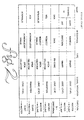
- Figure 2 is a signal chart setting forth the name, description, and signal characteristics for a high speed data communication bus in accordance with the present invention.
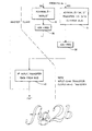
- Figures 2A and 2B illustrate a flow chart indicating the sequence of operation of a high speed data communication bus in accordance with the present invention.
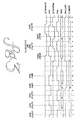
- Figure 3 is timing diagram illustrating the waveform of the signals described in the signal chart of figure 2.
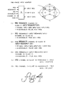
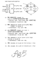
- Figure 4 is a state transition diagram for an embodiment of a two phase input adapter for an input data interface, including logic equations for the transitions between states, for a high speed data communication bus in accordance with the present invention.
- Figure 5 is a state transition diagram for an embodiment of a two phase output adapter for an output data interface, including logic equations for the transitions between states, for a high speed data communication bus in accordance with the present invention.
- a data communication bus 10 provides for high speed data communication between a master 12, typically a central processing unit (cpu), and a slave unit 14, typically a peripheral unit serving the central processing unit.
- the slave peripheral unit 14 includes a two phase input adapter 16 and two phase output adapter 18, which provide respective data input and data output interface between the bus 10 and the slave peripheral 14.
- the CHANNEL ID lines generated by the master are used to identify the communication channel.
- the CHANNEL ID is defined as the ADDRESS bits and the direction bit, DIR.
- the CHANNEL ID may contain 8 individual lines, or bits, allowing access to 256 communication channels.
- the CHANNEL ID includes one bit, DIR, to signify direction of the data transfer, either output or input.
- the remaining 7 data lines are address bits designating one of 128 channels, each of which can be used for both input and output, depending up on the state of direction control line DIR.
- DIR is equal to logic level low to indicate an output, and logic level high to indicate an input.
- the data lines are bi-directional, and can be any number of bits. Typically, the number of data lines are a multiple of 8 bits.
- the REQ signal which indicates a request for a data transfer, is generated by the master.
- the ACK signal which indicates acknowledgment of a request for a data transfer, is generated by the slave.
- the REQINVALID and ACKINVALID signals generated by the master and slave, respectively, indicate whether a respective REQ or ACK signal is valid or invalid.
- the REQINVALID signal which is generated by the master, is a logic 0 when the REQ signal is valid, and a logic 1 when the REQ signal is invalid.
- the ACKINVALID signal which is generated by the slave, is a logic 0 when the ACK signal is valid, and a logic 1 when the ACK signal is invalid.
- the REQ and ACK signals provide an indication by a transition between logic levels, either high to low, or low to high.
- the DATA lines are typically tri-state to provide for data transfer in either direction.
- open collector drivers are used to facilitate the connection of multiple slave devices to common control lines.
- the REQ and REQINVALID control lines originate from a dedicated master unit.
- the REQ and REQINVALID lines are open collector drivers. That is, where the bus master is not dedicated, but is selected among competing devices suitable contention mechanism, the REQ and REQINVALID lines can be open collector of tri-state so the more than one devices can share the control lines.
- a flow chart indicating the communication sequence between master and slave units is shown in figures 2A and 2B.
- the program is entered at step 20 whenever the master unit is to transfer data, either input or output. If the CHANNEL ID is unchanged from the last data transfer or the REQ line is high, then the master skips step 22 and proceeds to step 26 where the bus address and direction lines are set to the CHANNEL ID value, and, if the requested data transfer is a data output, then the bus DATA lines are set equal to the output data values.
- the REQ signal is toggled to the opposite value at step 28.
- the transition of the REQ signal is the indication that the master is requesting a data transfer.
- the REQINVALID line is set to "invalid", and the REQ signal is toggled at step 22, i.e. from low to high.
- the slave unit responds to the REQINVALID signal being high by setting the ACKINVALID signal to high i.e. "invalid", at step 24 indicating that the returning ACK signal is to be considered invalid.
- the ACK signal is set equal to the REQ signal. Since the ACK line was previously low, the ACK transition is from low to high. The bus is now in a reset state and ready for the new data transfer initiated at steps 26 and 28.
- the master signals a data transfer request REQ, at step 28.
- the slave receives the transition of the REQ signal generated at step 28 and decides whether or not it can accept the data transfer at step 30. If the data transfer cannot be accepted, the ACKINVALID line is set to "invalid" at step 32, and the ACK signal is set equal to the REQ signal at step 36.
- the ACK signal generated at step 36 by the slave indicates to the master that the slave cannot accept the data transfer, and that the master can now carry out other concurrent tasks. However, the master will eventually attempt to re-initiate the data transfer at a later time.
- the slave If at step 30 the slave is able to accept the data transfer, then the ACKINVALID line is set to "valid" at step 34, and the input or output data is transferred to or from the data bus respectively. Thereafter the ACK signal is set equal to the REQ signal at step 38. The transition of the ACK signal at step 38 at a time when ACKINVALID is low, indicates to the master that the data transfer is successful. If the data transfer is an input operation, the master transfers data from the bus at step 40.
- a failsafe timer to prevent the bus from coming to a halt when a peripheral unit fails to signal ACK through malfunction or absence, would function as follows:
- Figures 2a and 2b represent the programming performed in the master as well as the programming performed in the slave.
- the portion of the flow chart of figures 2a and 2b to the left of the dotted line is carried out by the master unit.
- the portion of the flow chart of figures 2a and 2b to the right half of the dotted line is carried out by the slave unit.
- the master unit is typically a central processing unit of a computer system, it is desirable that the program for the operation of the bus be embodied in microcode. An input or output operation by the bus master would then be accomplished in a single instruction of the main processing unit.
- the following program fragments, expressed in a pseudo code, similar to the Pascal programming language, may be used to implement super input or super output instructions for use on the communication bus of the present embodiment.
- a timing diagram illustrating the operation of the communication bus is shown in figure 3.
- the master sets the CHANNEL ID onto the address and direction lines at time A. Also at time A, the master places the data onto the DATA lines. Then, at time B, the master signals REQ by toggling the current value of REQ (high) to the opposite value (low). Then, at time C, the slave sets ACKINVALID equal to "valid", and signals back to the master indicating that the transfer was successful by a transition of the ACK signal (also from high to low).
- the next data transfer over the bus is to a different device, i.e. to a different address.
- the REQ and the ACK signal are low.
- the next device at the new address will not be able to easily bring the ACK line high because the former device which shares the ACK line, is holding it low.
- the master sets the REQINVALID line to "invalid”, and toggles the REQ line from low to high at time D.
- the slave sets its ACKINVALID line to "invalid” and toggles the ACK line from low to high at time E.
- the bus is now in a reset state.
- the bus can proceed to initiate an output data transfer.
- New address and data are placed on the ADDRESS, DIR and DATA lines at time F.
- the slave device is assumed to be busy or otherwise not ready to accept data at time F, and communicates such condition by setting the ACKINVALID high to "invalid". Therefore, at time G when the slave device signals its ACK line, the ACKINVALID is indicating to the master that the second peripheral device could not accept the output data. The master will later attempt to re-transmit the output data. In the meantime, the master is free to work on other concurrent tasks.
- the next data transfer over the bus is a data input from a different device. Since the REQ line and the ACK line just after point G are low, it is necessary to bring the bus to a reset conditions at time I, in the same manner as the bus was reset at time E.
- the new address is placed on the ADDRESS lines at time J, at which point the direction of data transfer ,DIR, is changed from output to input.
- the master signals a request, REQ at time K, and the designated slave unit places data on the DATA lines at time L. Thereafter, the slave unit provides an ACK transaction at time M in response to which data is input to the master.
- the description of the operation of the communication bus from time A to time M illustrates the operation of the data bus when the CHANNEL ID changes and the REQ line is low in between consecutive data transfers. Under the illustrated conditions thus far, the operation of the data bus is somewhat slower because of the need to condition the bus into a reset state between data transfers. However, so long as the CHANNEL ID remains the same or REQ line is high (even if the CHANNEL ID changes), then there is no need to reset the data bus, and the data transfer rate can continue at full bus speed.
- the interface between the central processing unit and the bus is best embodied in a microcoded instruction set for super input and output.
- the interface between the peripheral unit and the data bus may be implemented by the use of a two phase input adaptor 16 and a two phase output adaptor 18 as shown in block form in Figure 1.
- the two phase input adaptor 16 includes an initial state SO, and three other internal states S1, S2 and S3. Transitions between the four states is governed by transition control signals C0, C1, C2, C3, C4, and C5. For each of the logic equations given in Figure 4, the indicated transition takes place when the logical value given by the equations in Figure 4 indicate a true condition. Also at that time, when one of the conditions C0 through C5 become true, the lines to the right of the arrow indicate the desired operation of the interface with respect to the data bus.
- the two phase output adaptor 18 includes an initial state S0, and three other internal states S1, S2 and S3. Transitions between the four states is governed by transition control signals C0, C1, C2, C3, C4, and C5.
- the indicated transition takes place when the logical value given by the equations in Figure 5 indicate a true condition.
- the lines to the right of the arrow indicate the desired operation of the interface with respect to the data bus.
- the input adaptor 16 and two phase output adaptor 18 may be implemented by one skilled in the art using custom logic, programmable logic arrays or a general purpose embedded programmable microprocessor.
- the input adaptor interfaces to the bus of the present invention, and also acts as a receiver in the standard two-phase interface, as described above.
- the output adaptor interfaces to the present bus, and also acts as a sender for the standard two-phase interface.
Landscapes
- Engineering & Computer Science (AREA)
- Theoretical Computer Science (AREA)
- Physics & Mathematics (AREA)
- General Engineering & Computer Science (AREA)
- General Physics & Mathematics (AREA)
- Information Transfer Systems (AREA)
- Small-Scale Networks (AREA)
- Communication Control (AREA)
Claims (26)
- Verfahren zum Betreiben eines Kommunikationssystems, umfassend eine Master-Einheit (12) und eine Slave-Einheit (14), zwischen denen Daten übertragen werden können, wobei das Verfahren die folgenden Schritte umfaßt:Erzeugen, mit der genannten Master-Einheit (12), eines Übergangs zwischen zwei logischen Zuständen eines ersten Steuersignals (REQ) als Anzeige einer Datenübertragungsanforderung für die genannte Slave-Einheit, dadurch gekennzeichnet, daß:die genannte Master-Einheit vor dem genannten Übergang des ersten Steuersignals ein zweites Steuersignal (REQINVALID) erzeugt, dessen Zustand als Anzeige für die genannte Slave-Einheit dient, ob der genannte Übergang des ersten Steuersignals (REQ) eine gültige Anzeige ist oder nicht.
- Verfahren nach Anspruch 1, ferner umfassend den Schritt, bei dem die genannte Slave-Einheit (14) einen Übergang zwischen zwei logischen Zuständen eines dritten Steuersignals (ACK) als Anzeige der Annahme der genannten Anforderung für die genannte Master-Einheit (12) erzeugt, dadurch gekennzeichnet, daß:
die genannte Slave-Einheit vor dem genannten Übergang des dritten Steuersignals (ACK) ein viertes Steuersignal (ACKINVALID) erzeugt, dessen Zustand als Anzeige für die genannte Master-Einheit dient, ob der genannte Übergang des dritten Steuersignals (ACK) eine gültige Annahmeanzeige ist oder nicht. - Verfahren nach Anspruch 2, umfassend den Schritt des Eingebens von Daten in die genannte Master-Einheit, die von der genannten Slave-Einheit nach dem genannten Übergang des dritten Steuersignals (ACK) ausgegeben wurden, vorausgesetzt, daß das genannte vierte Steuersignal (ACKINVALID) eine gültige Annahmeanzeige anzeigt.
- Verfahren nach Anspruch 2, umfassend den Schritt des Eingebens von Daten in die genannte Slave-Einheit (14), die von der genannten Master-Einheit (12) nach dem genannten Übergang des genannten ersten Steuersignals (REQ) ausgegeben wurden, vorausgesetzt, daß das genannte zweite Steuersignal (REQINVALID) eine gültige Anforderung anzeigt.
- Verfahren nach Anspruch 1, 2, 3 oder 4, umfassend den Schritt, daß die genannte Master-Einheit (12) ein Signal (DIR) an die genannte Slave-Einheit (14) anlegt, um die Übertragungsrichtung der das Subjekt der genannten Anforderung darstellenden Daten zwischen den Einheiten anzuzeigen.
- Verfahren nach einem der vorherigen Ansprüche, angewandt in einem Kommunikationssystem, bei dem die genannte Slave-Einheit (14) eine aus einer Mehrzahl von Slave-Einheiten ist, die auf gleichartige Weise betrieben und für die Übertragung von Daten zwischen einer ausgewählten Slave-Einheit und der genannten Master-Einheit (12) ausgewählt werden können, und umfassend den Schritt, daß die genannte Master-Einheit (12) ein Signal (ADDR) für die Auswahl einer aus der genannten Mehrzahl von Slave-Einheiten erzeugt, um eine Datenübertragung damit anzufordern.
- Verfahren nach Anspruch 6, bei dem jede aus der genannten Mehrzahl von Slave-Einheiten eine individuelle Adresse hat und das von der genannten Master-Einheit (12) erzeugte Signal (ADDR) für die Auswahl einer Slave-Einheit deren Adresse umfaßt.
- Kommunikationssystem, umfassend eine Master-Einheit (12) und eine Slave-Einheit (14), zwischen denen Daten übertragen werden können, wobei die genannte Master-Einheit (12) betrieben werden kann, um einen Übergang zwischen zwei logischen Zuständen eines ersten Steuersignals (REQ) als Anzeige einer Datenübertragungsanforderung für die genannte Slave-Einheit (14) zu erzeugen, dadurch gekennzeichnet, daß:
die genannte Master-Einheit (12) betrieben werden kann, um vor dem Übergang des ersten Steuersignals (REQ) ein zweites Steuersignal (REQINVALID) zu erzeugen, dessen Zustand als Anzeige für die genannte Slave-Einheit (14) dient, ob der genannte Übergang des ersten Steuersignals eine gültige Anzeige ist oder nicht. - System nach Anspruch 8, bei dem die genannte Slave-Einheit (14) betrieben werden kann, um einen Übergang zwischen zwei logischen Zuständen eines dritten Steuersignals (ACK) als Anzeige der Annahme der genannten Anforderung für die genannte Master-Einheit (12) zu erzeugen, dadurch gekennzeichnet, daß:
die genannte Slave-Einheit (14) betrieben werden kann, um vor dem genannten Übergang des dritten Steuersignals (ACK) ein viertes Steuersignal (ACKINVALID) zu erzeugen, dessen Zustand als Anzeige für die genannte Master-Einheit (12) dient, ob der genannte Übergang des dritten Steuersignals (ACK) eine gültige Annahmeanzeige ist oder nicht. - System nach Anspruch 9, bei dem Daten, die von der genannten Slave-Einheit (14) ausgegeben wurden, von der genannten Master-Einheit (12) nach dem Übergang des genannten dritten Steuersignals (ACK) eingegeben werden, vorausgesetzt, daß das genannte vierte Steuersignal (ACKINVALID) eine gültige Annahmeanzeige anzeigt.
- System nach Anspruch 9, bei dem Daten, die von der genannten Master-Einheit (12) ausgegeben wurden, von der genannten Slave-Einheit (14) nach dem genannten Übergang des genannten ersten Steuersignals (REQ) eingegeben werden, vorausgesetzt, daß das genannte zweite Steuersignal (REQINVALID) eine gültige Anforderung anzeigt.
- System nach Anspruch 8, 9, 10 oder 11, bei dem die genannte Master-Einheit (12) betrieben werden kann, um ein Signal (DIR) an die genannte Slave-Einheit (14) anzulegen, das die Übertragungsrichtung der das Subjekt der genannten Anforderung darstellenden Daten zwischen den Einheiten anzeigt.
- System nach einem der Ansprüche 8 bis 12, bei dem die genannte Slave-Einheit (14) eine aus einer Mehrzahl von Slave-Einheiten ist, die auf gleichartige Weise betrieben und für die Übertragung von Daten zwischen einer ausgewählten Slave-Einheit und der genannten Master-Einheit (12) ausgewählt werden können, wobei die genannte Master-Einheit (12) so betrieben werden kann, daß sie ein Signal (ADDR) für die Auswahl einer aus der genannten Mehrzahl von Slave-Einheiten erzeugt.
- System nach Anspruch 13, bei dem jede aus der genannten Mehrzahl von Slave-Einheiten eine individuelle Adresse hat und die genannte Master-Einheit (12) so betrieben werden kann, daß sie die Adresse (RDDR) einer Slave-Einheit für deren Auswahl erzeugt.
- Master-Einheit (12) für die Verwendung mit einer Slave-Einheit (14) in einem Kommunikationssystem, bei dem Daten zwischen der Master-Einheit (12) und der Slave-Einheit (14) übertragen werden können, wobei die genannte Master-Einheit (12) betrieben werden kann, um einen Übergang zwischen zwei logischen Zuständen eines ersten Steuersignals (REQ) als Anzeige einer Datenübertragungsanforderung dazwischen für eine Slave-Einheit (14) zu erzeugen, dadurch gekennzeichnet, daß:
die genannte Master-Einheit (12) betrieben werden kann, um vor dem genannten Übergang des genannten Steuersignals (REQ) ein zweites Steuersignal (REQINVALID) als Anzeige für eine Slave-Einheit (14) zu erzeugen, daß der genannte Übergang des ersten Steuersignals (REQ) eine gültige Anzeige ist. - Master-Einheit (12) nach Anspruch 15, die betrieben werden kann, um Daten zur Übertragung zu einer Slave-Einheit auszugeben, und um einen Übergang des genannten ersten Steuersignals (REQ) zu erzeugen, der durch den Zustand des genannten zweiten Steuersignals (REQINVALID) als gültig angezeigt wird, wobei die Master-Einheit ferner dazu betrieben werden kann, um auf den Eingang eines Übergangs zwischen zwei logischen Zuständen eines dritten Steuersignals (ACK) in Anwesenheit des Eingangs eines vierten Steuersignals (ACKINVALID) anzusprechen, dessen Zustand als Anzeige dafür dient, ob der genannte Übergang des dritten Steuersignals (ACK) gültig ist oder nicht, um zu erkennen, ob die Datenübertragung erfolgte oder nicht.
- Master-Einheit (12) nach Anspruch 15, die betrieben werden kann, um Daten in Reaktion auf den Eingang eines Übergangs eines dritten Steuersignals (ACK) in Anwesenheit des Eingangs eines vierten Steuersignals (ACKINVALID) einzugeben, dessen Zustand eine Anzeige dafür gibt, ob der genannte Übergang des dritten Steuersignals (ACK) eine gültige Anzeige ist oder nicht, wobei die Master-Einheit (12) die genannten Daten nur in Anwesenheit einer gültigen Anzeige eingibt.
- Master-Einheit nach Anspruch 13, 14, 15 oder 16, die betrieben werden kann, um ein Ausgangssignal anzulegen, das die Übertragungsrichtung von Daten zwischen der Master-Einheit und einer in Kommunikation mit dieser stehenden Slave-Einheit anzuzeigen.
- Master-Einheit nach einem der Ansprüche 15 bis 18, die betrieben werden kann, um ein Auswahlsignal (ADDR) zum Auswählen einer aus einer Mehrzahl von Slave-Einheiten in einem Kommunikationssystem zu erzeugen.
- Master-Einheit nach Anspruch 19, bei der das genannte Auswahlsignal (ADDR) eine ausgewählte eine aus einer Mehrzahl von Adressen umfaßt.
- Slave-Einheit (14) zur Verwendung mit einer Master-Einheit (12) in einem Kommunikationssystem, bei dem Daten zwischen der Slave-Einheit (14) und der Master-Einheit (12) übertragen werden können, wobei die genannte Slave-Einheit (14) auf den Übergang zwischen zwei logischen Zuständen eines ersten Steuersignals (REQ) anspricht, das als Anzeige einer Anforderung für die Übertragung von Daten daran angelegt wird, und die so betrieben werden kann, daß sie einen Übergang zwischen zwei logischen Pegeln eines zweiten Steuersignals (ACK) ausgibt, um die Annahme der genannten Anforderung anzuzeigen, dadurch gekennzeichnet, daß:
die genannte Slave-Einheit betrieben werden kann, um ein drittes Steuersignal (ACKINVALID) vor der Ausgabe des genannten Übergangs des zweiten Steuersignals (ACK) auszugeben, dessen Zustand eine Anzeige dafür ist, ob der genannte Übergang des zweiten Steuersignals (ACK) eine gültige Annahmeanzeige ist oder nicht. - Slave-Einheit (14) nach Anspruch 21, die auf ein viertes Steuersignal (REQINVALID) anspricht, dessen Zustand zum Zeitpunkt des genannten Übergangs des ersten Steuersignals (REQ) anzeigt, ob der genannte Übergang des ersten Steuersignals (REQ) eine gültige Anforderung anzeigt oder nicht.
- Slave-Einheit (12) nach Anspruch 22, die betrieben werden kann, um Daten zum Zeitpunkt des Übergangs des genannten ersten Steuersignals (REQ) einzugeben oder auszugeben, vorausgesetzt, daß der Zustand des genannten vierten Steuersignals (REQINVALID) eine gültige Anforderung anzeigt.
- Slave-Einheit (14) nach Anspruch 21, 22 oder 23, die auf ein Eingangssignal (DIR) anspricht, das die Datenübertragungsrichtung zwischen der Slave-Einheit (14) und einer Master-Einheit (12) anzeigt.
- Slave-Einheit (14) nach einem der Ansprüche 18 bis 22, die auf den Eingang eines Auswahlsignals (ADDR) anspricht, um die Slave-Einheit (14) zu befähigen, auf einen Übergang des daran angelegten genannten ersten Steuersignals (REQ) anzusprechen.
- Slave-Einheit nach Anspruch 25, die eine individuelle Adresse beinhaltet und auf ein Auswahlsignal reagiert, das die Adresse der Slave-Einheit trägt.
Applications Claiming Priority (2)
| Application Number | Priority Date | Filing Date | Title |
|---|---|---|---|
| US697863 | 1991-05-09 | ||
| US07/697,863 US5404137A (en) | 1991-05-09 | 1991-05-09 | High speed transition signalling communication system |
Publications (3)
| Publication Number | Publication Date |
|---|---|
| EP0514080A2 EP0514080A2 (de) | 1992-11-19 |
| EP0514080A3 EP0514080A3 (en) | 1994-06-22 |
| EP0514080B1 true EP0514080B1 (de) | 1999-12-01 |
Family
ID=24802897
Family Applications (1)
| Application Number | Title | Priority Date | Filing Date |
|---|---|---|---|
| EP92304102A Expired - Lifetime EP0514080B1 (de) | 1991-05-09 | 1992-05-07 | Übergangssignalisierende Datenkommunikationen |
Country Status (5)
| Country | Link |
|---|---|
| US (1) | US5404137A (de) |
| EP (1) | EP0514080B1 (de) |
| JP (1) | JPH05153192A (de) |
| CA (1) | CA2066020A1 (de) |
| DE (1) | DE69230353T2 (de) |
Families Citing this family (9)
| Publication number | Priority date | Publication date | Assignee | Title |
|---|---|---|---|---|
| US6256694B1 (en) * | 1994-06-30 | 2001-07-03 | Compaq Computer Corporation | Distributed early arbitration |
| CA2158588C (en) * | 1994-09-21 | 2003-01-14 | Belwinder Singh Barn | Multiple channel terminal server communications network |
| EP0738096B1 (de) * | 1994-10-31 | 2006-03-01 | Daikin Industries, Ltd. | Sender |
| EP0752666A3 (de) * | 1995-07-06 | 2004-04-28 | Sun Microsystems, Inc. | Verfahren und Vorrichtung zur Beschleunigung von Sklave-Anforderungen in einem paketvermittelten Computersystem |
| US5909369A (en) * | 1996-07-24 | 1999-06-01 | Network Machines, Inc. | Coordinating the states of a distributed finite state machine |
| US6275883B1 (en) | 1999-01-15 | 2001-08-14 | Advanced Memory International, Inc. | Contention-free signaling scheme for shared control signals |
| US7043577B2 (en) * | 2002-08-27 | 2006-05-09 | General Electric Company | Auto-detecting universal appliance communication controller |
| JP4650566B2 (ja) * | 2008-12-22 | 2011-03-16 | 株式会社デンソー | 制御システム及び電子制御装置 |
| JP5152258B2 (ja) * | 2010-06-21 | 2013-02-27 | 株式会社デンソー | 制御システム及び通信機能付センサ装置及び電子制御装置 |
Family Cites Families (13)
| Publication number | Priority date | Publication date | Assignee | Title |
|---|---|---|---|---|
| US3886524A (en) * | 1973-10-18 | 1975-05-27 | Texas Instruments Inc | Asynchronous communication bus |
| US3993981A (en) * | 1975-06-30 | 1976-11-23 | Honeywell Information Systems, Inc. | Apparatus for processing data transfer requests in a data processing system |
| US4085448A (en) * | 1976-10-04 | 1978-04-18 | International Business Machines Corporation | Data communication bus structure |
| US4300193A (en) * | 1979-01-31 | 1981-11-10 | Honeywell Information Systems Inc. | Data processing system having data multiplex control apparatus |
| US4300194A (en) * | 1979-01-31 | 1981-11-10 | Honeywell Information Systems Inc. | Data processing system having multiple common buses |
| US4495571A (en) * | 1979-01-31 | 1985-01-22 | Honeywell Information Systems Inc. | Data processing system having synchronous bus wait/retry cycle |
| EP0087664B1 (de) * | 1980-02-04 | 1985-09-11 | Xerox Corporation | Phasendekodierer für Datenübermittlungssysteme |
| US4370712A (en) * | 1980-10-31 | 1983-01-25 | Honeywell Information Systems Inc. | Memory controller with address independent burst mode capability |
| US4558429A (en) * | 1981-12-17 | 1985-12-10 | Honeywell Information Systems Inc. | Pause apparatus for a memory controller with interleaved queuing apparatus |
| US4967344A (en) * | 1985-03-26 | 1990-10-30 | Codex Corporation | Interconnection network for multiple processors |
| FR2586118B1 (fr) * | 1985-08-06 | 1990-01-05 | Bull Sems | Procede d'echange de donnees entre un microprocesseur et une memoire et dispositif permettant la mise en oeuvre du procede |
| US4969121A (en) * | 1987-03-02 | 1990-11-06 | Altera Corporation | Programmable integrated circuit logic array device having improved microprocessor connectability |
| US4962378A (en) * | 1987-11-09 | 1990-10-09 | Ncr Corporation | Multi-user serial bus system |
-
1991
- 1991-05-09 US US07/697,863 patent/US5404137A/en not_active Expired - Fee Related
-
1992
- 1992-04-14 CA CA002066020A patent/CA2066020A1/en not_active Abandoned
- 1992-05-07 DE DE69230353T patent/DE69230353T2/de not_active Expired - Fee Related
- 1992-05-07 EP EP92304102A patent/EP0514080B1/de not_active Expired - Lifetime
- 1992-05-08 JP JP4115784A patent/JPH05153192A/ja active Pending
Also Published As
| Publication number | Publication date |
|---|---|
| EP0514080A3 (en) | 1994-06-22 |
| US5404137A (en) | 1995-04-04 |
| DE69230353T2 (de) | 2000-07-27 |
| JPH05153192A (ja) | 1993-06-18 |
| CA2066020A1 (en) | 1992-11-10 |
| EP0514080A2 (de) | 1992-11-19 |
| DE69230353D1 (de) | 2000-01-05 |
Similar Documents
| Publication | Publication Date | Title |
|---|---|---|
| EP0165600B1 (de) | Ein-/Ausgabebus für Rechner | |
| US5233692A (en) | Enhanced interface permitting multiple-byte parallel transfers of control information and data on a small computer system interface (SCSI) communication bus and a mass storage system incorporating the enhanced interface | |
| EP0476990B1 (de) | Dynamische Busarbitrierung | |
| US4868742A (en) | Input/output bus for system which generates a new header parcel when an interrupted data block transfer between a computer and peripherals is resumed | |
| US5019966A (en) | Dual processors using busy signal for controlling transfer for predetermined length data when receiving processor is processing previously received data | |
| EP0386935B1 (de) | Gerät, das fähig ist, die Anzahl von Wartezuständen für den Zugriff zu variieren | |
| EP0030978B1 (de) | Steuersystem für datenübertragung | |
| JPH0619755B2 (ja) | アービトレーシヨンを制御するための方法及び装置 | |
| US4120029A (en) | Method and apparatus for recovering a signal transferred over a common bus in a data processing system | |
| JPH0217818B2 (de) | ||
| US5404137A (en) | High speed transition signalling communication system | |
| US6175887B1 (en) | Deterministic arbitration of a serial bus using arbitration addresses | |
| US3999170A (en) | Multiple access interconnect system | |
| JPS586177B2 (ja) | インタ−フエ−ス回路の選択システム | |
| US5797040A (en) | Computer system having system bus which couples adapter and processing units and requires acquisition for data transmission thereover | |
| JP3399776B2 (ja) | コンピュータおよびコンピュータにおける周辺デバイス制御データの転送方法 | |
| US5303345A (en) | Method for controlling data sending and receiving operations of a microprocessor | |
| JPH05282242A (ja) | バス制御方式 | |
| JP2000244585A (ja) | バスインタフェース回路 | |
| JPS61251252A (ja) | デ−タ転送処理方法 | |
| JP2752456B2 (ja) | チャネル装置 | |
| JPS60183659A (ja) | 情報転送制御方式 | |
| JP2924232B2 (ja) | コマンドチェック装置 | |
| JP2615815B2 (ja) | 優先順位制御方式 | |
| JP3423376B2 (ja) | 情報処理装置及びその制御方法 |
Legal Events
| Date | Code | Title | Description |
|---|---|---|---|
| PUAI | Public reference made under article 153(3) epc to a published international application that has entered the european phase |
Free format text: ORIGINAL CODE: 0009012 |
|
| AK | Designated contracting states |
Kind code of ref document: A2 Designated state(s): DE FR GB IT |
|
| PUAL | Search report despatched |
Free format text: ORIGINAL CODE: 0009013 |
|
| AK | Designated contracting states |
Kind code of ref document: A3 Designated state(s): DE FR GB IT |
|
| 17P | Request for examination filed |
Effective date: 19941221 |
|
| 17Q | First examination report despatched |
Effective date: 19970623 |
|
| GRAG | Despatch of communication of intention to grant |
Free format text: ORIGINAL CODE: EPIDOS AGRA |
|
| GRAG | Despatch of communication of intention to grant |
Free format text: ORIGINAL CODE: EPIDOS AGRA |
|
| GRAH | Despatch of communication of intention to grant a patent |
Free format text: ORIGINAL CODE: EPIDOS IGRA |
|
| GRAH | Despatch of communication of intention to grant a patent |
Free format text: ORIGINAL CODE: EPIDOS IGRA |
|
| GRAA | (expected) grant |
Free format text: ORIGINAL CODE: 0009210 |
|
| AK | Designated contracting states |
Kind code of ref document: B1 Designated state(s): DE FR GB IT |
|
| PG25 | Lapsed in a contracting state [announced via postgrant information from national office to epo] |
Ref country code: IT Free format text: LAPSE BECAUSE OF FAILURE TO SUBMIT A TRANSLATION OF THE DESCRIPTION OR TO PAY THE FEE WITHIN THE PRE;WARNING: LAPSES OF ITALIAN PATENTS WITH EFFECTIVE DATE BEFORE 2007 MAY HAVE OCCURRED AT ANY TIME BEFORE 2007. THE CORRECT EFFECTIVE DATE MAY BE DIFFERENT FROM THE ONE RECORDED.SCRIBED TIME-LIMIT Effective date: 19991201 Ref country code: FR Free format text: LAPSE BECAUSE OF FAILURE TO SUBMIT A TRANSLATION OF THE DESCRIPTION OR TO PAY THE FEE WITHIN THE PRESCRIBED TIME-LIMIT Effective date: 19991201 |
|
| REF | Corresponds to: |
Ref document number: 69230353 Country of ref document: DE Date of ref document: 20000105 |
|
| EN | Fr: translation not filed | ||
| PG25 | Lapsed in a contracting state [announced via postgrant information from national office to epo] |
Ref country code: GB Free format text: LAPSE BECAUSE OF NON-PAYMENT OF DUE FEES Effective date: 20000507 |
|
| PLBE | No opposition filed within time limit |
Free format text: ORIGINAL CODE: 0009261 |
|
| STAA | Information on the status of an ep patent application or granted ep patent |
Free format text: STATUS: NO OPPOSITION FILED WITHIN TIME LIMIT |
|
| 26N | No opposition filed | ||
| GBPC | Gb: european patent ceased through non-payment of renewal fee |
Effective date: 20000507 |
|
| PG25 | Lapsed in a contracting state [announced via postgrant information from national office to epo] |
Ref country code: DE Free format text: LAPSE BECAUSE OF NON-PAYMENT OF DUE FEES Effective date: 20010301 |