EP0514818B1 - Dispositif amplificateur programmable - Google Patents
Dispositif amplificateur programmable Download PDFInfo
- Publication number
- EP0514818B1 EP0514818B1 EP92108371A EP92108371A EP0514818B1 EP 0514818 B1 EP0514818 B1 EP 0514818B1 EP 92108371 A EP92108371 A EP 92108371A EP 92108371 A EP92108371 A EP 92108371A EP 0514818 B1 EP0514818 B1 EP 0514818B1
- Authority
- EP
- European Patent Office
- Prior art keywords
- gain
- stage
- circuit
- stages
- transistor
- Prior art date
- Legal status (The legal status is an assumption and is not a legal conclusion. Google has not performed a legal analysis and makes no representation as to the accuracy of the status listed.)
- Expired - Lifetime
Links
- 102220128896 rs376207606 Human genes 0.000 claims description 9
- 102200126521 rs4498440 Human genes 0.000 claims description 4
- 102220473072 Chemerin-like receptor 2_R14Q_mutation Human genes 0.000 claims description 3
- 238000006243 chemical reaction Methods 0.000 claims description 2
- 102220605470 Coilin_R15A_mutation Human genes 0.000 claims 1
- 102220503972 Endogenous retrovirus group K member 6 Rec protein_R16A_mutation Human genes 0.000 claims 1
- 230000003321 amplification Effects 0.000 description 7
- 238000003199 nucleic acid amplification method Methods 0.000 description 7
- 102220465933 Beta-1,3-glucuronyltransferase LARGE2_R15A_mutation Human genes 0.000 description 6
- 230000006835 compression Effects 0.000 description 6
- 238000007906 compression Methods 0.000 description 6
- 230000033228 biological regulation Effects 0.000 description 5
- 230000000694 effects Effects 0.000 description 5
- 230000006978 adaptation Effects 0.000 description 3
- 238000002513 implantation Methods 0.000 description 3
- 238000009413 insulation Methods 0.000 description 3
- 230000010355 oscillation Effects 0.000 description 3
- 239000000758 substrate Substances 0.000 description 3
- 238000002955 isolation Methods 0.000 description 2
- 238000000034 method Methods 0.000 description 2
- 230000007704 transition Effects 0.000 description 2
- 238000013519 translation Methods 0.000 description 2
- JBRZTFJDHDCESZ-UHFFFAOYSA-N AsGa Chemical compound [As]#[Ga] JBRZTFJDHDCESZ-UHFFFAOYSA-N 0.000 description 1
- 229910017214 AsGa Inorganic materials 0.000 description 1
- 230000000712 assembly Effects 0.000 description 1
- 238000000429 assembly Methods 0.000 description 1
- 239000003990 capacitor Substances 0.000 description 1
- 239000000470 constituent Substances 0.000 description 1
- 238000013461 design Methods 0.000 description 1
- 235000021183 entrée Nutrition 0.000 description 1
- 230000006641 stabilisation Effects 0.000 description 1
- 238000011105 stabilization Methods 0.000 description 1
- 230000003797 telogen phase Effects 0.000 description 1
- 238000012360 testing method Methods 0.000 description 1
- 238000012546 transfer Methods 0.000 description 1
Images


Classifications
-
- H—ELECTRICITY
- H03—ELECTRONIC CIRCUITRY
- H03G—CONTROL OF AMPLIFICATION
- H03G3/00—Gain control in amplifiers or frequency changers
- H03G3/001—Digital control of analog signals
-
- H—ELECTRICITY
- H03—ELECTRONIC CIRCUITRY
- H03G—CONTROL OF AMPLIFICATION
- H03G1/00—Details of arrangements for controlling amplification
- H03G1/0005—Circuits characterised by the type of controlling devices operated by a controlling current or voltage signal
- H03G1/0088—Circuits characterised by the type of controlling devices operated by a controlling current or voltage signal using discontinuously variable devices, e.g. switch-operated
Definitions
- the invention relates to a programmable amplifier which can, in particular, be produced in the form of an integrated circuit of the type Analog ASIC (Application Specific Integrated circuit) for amplification applications in the telecommunications sector spatial.
- Analog ASIC Application Specific Integrated circuit
- the object of the device of the invention is to allow gain amplification of between 2 n and 2 n-1 in steps of 2 p with p ⁇ n; n being the number of bits of the gain control.
- Another solution is to cascade several amplifiers; the first amplifier with a high gain for get the best signal-to-noise ratio. But then the bandwidth is greatly reduced.
- the device of the invention includes an input stage which has a fixed gain and stages amplification having two switchable gain values; a floor output adapter; two current regulation circuits allowing to use a current variation law allowing to compensate for the gain variations of the different floors; the first circuit never being inhibited, and the second being controlled by the On / Off command.
- the entrance floor includes two branches arranged in parallel between supply voltage and ground; each branch comprising in series a resistor, a transistor, two transistors in parallel receiving a signal delivered by the first circuit of current regulation, two resistors in the middle of which is an entry point.
- Each switchable gain amplifier stage includes two branches arranged in parallel, each branch each comprising a resistor, a first transistor and a second transistor with two transmitters; these two branches being connected to the two inputs of a switching circuit through two resistors; himself being connected to ground through a third transistor which receives a signal from the second current regulation circuit operating as a DC generator; input interface circuits connected respectively to the base of each second transistor two transmitters for level translation for cascade the floors between them; a voltage comparator circuit which receives a signal from the first current regulation circuit allowing to select the gain of the stage.
- Such a device makes it possible to meet the gain objectives, bandwidth, noise factor defined above.
- the factor of noise in particular, is greatly improved for low gains.
- the device of the invention comprises several amplifier stages, here 7 in number, Ao, A1, A2, A3, A4, A5, A6 each with two inputs and two outputs allowing operation in symmetrical mode.
- Each of these stages Ao to A6 is supplied between a voltage Vc and mass.
- the stages A1 to A6 have two switchable gain values thanks to an external command Ci: here bits C3, C2, C42, C41, C1 and Co.
- Ci an external command
- the first stage Ao has a fixed gain. Two floors per example A3 and A4 are identical in winning states.
- An output of stage A6 is connected to an adapter stage of output A7 followed by a resistor R7, for example of value 50 OHMS.
- Transistors To to T6 each connected to ground through of a resistance Ro to R6 allow compensation to be made by temperature of the gain variation of each of the stages Ao to A6, in delivering them an appropriate tension.
- Two regulation circuits stream 10 and 11, like “Bandgap" for example, allow to use a current variation law making it possible to carry out this compensation for temperature variations of the gains of these different floors.
- the first of these two circuits can be called “master” and the second "slave”.
- the master circuit 10 generates a signal V2 serving reference voltage of the input stage Ao and threshold voltages for the comparator circuits 12 which exist in stages A1 to A6 as shown in FIG. 3. This circuit 10 is never inhibited.
- the slave circuit 11 generates a signal V3 serving as a voltage reference of stages A1 to A6, and driving the current generators of these stages, which are the T14 transistors shown in the figure 3.
- This circuit can be inhibited by the M / A (On / Off) command.
- the stages A1 to A6 are no longer supplied. They don't therefore work more; which allows both to isolate the inputs El, E2 of the output S.
- the input and output impedances remain, however, maintained at 50 OHMS, stages Ao and A7 still being powered.
- this device is produced in the form of an ASIC.
- the stage Ao has a fixed gain to improve the factor noise from the complete chain.
- This stage is optimized in gain and frequency.
- the gain value of this stage compensates for both the attenuation provided by stages A3 and A4 (-6 dB) and by the stage A6 which is due to the transition from the symmetrical mode at the input thereof to an asymmetric mode at the input of the output stage A7, and by the impedance matching between this stage A7 and the output load, for example 50 OHMS.
- such a device achieves a maximum gain value of 47 dB at output asymmetrical with 6 control bits as shown in the table I at the end of the description.
- the device of the invention is such that its maximum gain is greater than the maximum gain obtained with 5 bits of external control, but less than the gain maximum obtained with 6 bits.
- the device of the invention has a gain of between 2 n and 2 n-1 , n being the number of bits of the gain control.
- Each stage, including the entrance stage, has a maximum gain of less than 2 n-1 .
- the maximum value of the gain of stages A1 to A6 is 13 dB which makes it possible to obtain a passband of 440 MHz for the stage of 13 dB.
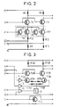
- FIG. 2 An exemplary embodiment of the input stage Ao is shown in FIG. 2.
- This stage then comprises two branches arranged in parallel between the supply voltage Vc and the ground; each branch each comprising in series a resistor R8 (R9) a transistor T8 (T9) which receives a bias voltage on its base continuous VP, two transistors in parallel T10, T10 '(T11, T11'), two resistors R10 and R11 (R12 and R13).
- This structure is optimized to obtain the best response in frequency (bandwidth), the best noise factor and for minimize the effects, due to the necessary adaptation between transistors ("Matching"), on the continuous offset of the floor.
- the transistors T10 and T11 are chosen for their low resistance rbb 'and their low resistance of transmitter access RE; these values being reduced by the fact of doubling the transistors (Transistors T10 and T10 'in parallel: transistors T11 and T11 'in parallel) which also has the effect of improving adaptation ("Matching") between transistors T10 and T11 by probability.
- transistors T10 (T10 ') and T11 (T11') are used continuously to current generators for the transistors T8 and T9 so as to obtain currents which vary in temperature adequately to keep the gain of the floor constant. This is obtained in applying a "bandgap" voltage of 1.2 volts on the bases of the transistors T10 and T11.
- the noise of a voltage-controlled common base assembly is important because the noise generated by the resistors rbb 'and RE and the collector current IC find a path through the source herself. But the transistors T10 (T10 ') and T11 (T11') are followed transistors T8 and T9 also mounted in common base. The load resistors R8 and R9 of these transistors, of higher values strong (for example 567 OHMS), are necessary to achieve the gain upstairs. The frequency effects of the Cjs and Cjc abilities are more important and require the use of faster transistors for example of type QN1 whose characteristics are given on the table II at the end of the description. The control of these transistors being this time a current command therefore a source of strong resistance internal. The noises generated by the resistors rbb ', RE and the current collector can no longer find a path and remain inactive. Only the base current generates noise at the output.
- resistors R10 and R12 associated with the resistors RE and dynamic transmitter access re transistors T10 (T10 ') and T11 (T11 '), allow to obtain an input impedance of 50 OHMS and improve the linearity of the input stage.
- the gain of this floor is the ratio between the load resistance R8 (or R9) and the sum of the resistance R10, (R12) and (RE + re + (rbb '/ BETA)) of transistors T10 and T11.
- This circuit removes the noises from transistors T8 and T9, reducing the stray capacitances collector / substrate.
- variable gain stages A1 to A6 An embodiment of the variable gain stages A1 to A6 is shown in Figure 3.
- Such a stage comprises two branches arranged in parallel, each branch each comprising a resistor R14A (R14B), a transistor T12A (T12B) and a transistor with two transmitters T13A (T13B); these two branches being connected to the two inputs of a switching circuit 13 through two resistors R15A and R16A (R15B and R16B); itself being connected to ground at through a T14 transistor operating as a generator direct current.
- Input interface circuits 14, 15 make it possible to produce a level translation to cascade the floors between them.
- the circuit 12 is a voltage comparator which allows to select the floor gain.
- Transistor T14 allows stabilization in temperature of the gain of the stage.
- T12A and T12B transistors limit the effects capacitive of transistors T13A and T13B (Cjs and Cjc). These transistors T12A and T12B do not contribute to increasing the noise figure of the floor.
- the resistances are all less than 1KILOHM. They are chosen to optimize the problems of "Matching".
- such a device makes it possible to produce a amplification function in the VHF domain with programming of the gain from 0 dB to 47 dB in 1 dB steps.
- Noise factor and point compression which represents a difference of 1 dB towards the bottom of the output signal / input signal transfer function with respect to an ideal linearity line, are very good.
- Impedances input and output are 50 OHMS, control inputs are TTL and CMOS compatible.
- the circuit can be put in a phase rest with sufficient input-output insulation; impedances entry-exit accesses keeping their initial values.
- the device of the invention has been produced in the form of an analog ASIC using bipolar technology so as to operate at VHF frequencies. But it could be increased in frequency up to a few tens of GHz in monolithic technology of the AsGa type.
- External controls Gain adjustment C0 C1 C2 C3 C41 C42 0 0 0 0 0 0 0 Reference 1 0 0 0 0 0 1 dB 0 1 0 0 0 0 2 dB 0 0 1 0 0 0 4 dB 0 0 0 1 0 0 8 dB 0 0 0 0 0 1 0 16 dB 0 0 0 0 0 0 1 16 dB
- QN1 QN2 Ft transition frequency
- 2.5 GHz 2.5 GHz re 24 ohms 21 ohms rbb ' 260 ohms 150 ohms Cjc 128 fF (1fF 10 -15 F
Landscapes
- Amplifiers (AREA)
- Tone Control, Compression And Expansion, Limiting Amplitude (AREA)
- Control Of Amplification And Gain Control (AREA)
Description
- la précision des résistances ;
- la bande passante ;
- les composants de commutation.
- la bande passante ;
- le facteur de bruit ;
- le point de compression ;
- le "matching" (adaptation) entre transistors.
- la figure 1 représente une réalisation du dispositif selon l'invention ;
- les figures 2 et 3 représentent deux réalisations de circuit du dispositif selon l'invention ;
- la figure 4 représente un jeu de courbes de réponse du dispositif selon l'invention.
| Ao | 18 dB |
| A1 | 8 dB ou 0 dB |
| A2 | 4 dB ou 0 dB |
| A3 = A4 | 13 dB ou - 3 dB |
| A5 | 2 dB ou 0 dB |
| A6 | 1 dB ou 0 dB. |
- de la résistance rbb' (résistance d'accès base);
- des capacités collecteur-substrat Cjs et collecteur-base Cjc. La charge de ces transistors étant la résistance dynamique re des transistors T8 et T9 qui est faible ( par exemple 24 OHMS). Cet effet est donc limité.
- avec les composants T13A, T13B, R15A, R15B on obtient une valeur minimun du gain, par exemple ;
- avec les composants T13A, T13B, R16A, R16B on obtient une valeur maximum du gain.
- Les masses des étages d'entrée et de sortie pour éviter tout rebouclage à cause de la résistance et de la self des fils de liaison ;
- Les tensions d'alimentation VC et VCS : on a connecté tous les "caissons" des résistances à la tension VC et non à la tension VCS pour éviter un rebouclage des signaux présents sur la ligne VCS vers la masse à cause de la capacité caisson-substrat et des fils de liaison. Ceci entraínerait sinon une oscillation HF pour les fortes valeurs de gain ainsi qu'une mauvaise isolation entrée-sortie en phase de repos.
- une bande passante de 270 MHz pour un gain maximum de 47 dB soit un produit gain-bande passante de l'ordre de 60 GHz ;
- un facteur de bruit au gain maximum de 10 dB environ ;
- un point de compression de l'ordre de 0 dBM.
| Commandes extérieures | Réglage du gain | |||||
| C0 | C1 | C2 | C3 | C41 | C42 | |
| 0 | 0 | 0 | 0 | 0 | 0 | Référence |
| 1 | 0 | 0 | 0 | 0 | 0 | 1 dB |
| 0 | 1 | 0 | 0 | 0 | 0 | 2 dB |
| 0 | 0 | 1 | 0 | 0 | 0 | 4 dB |
| 0 | 0 | 0 | 1 | 0 | 0 | 8 dB |
| 0 | 0 | 0 | 0 | 1 | 0 | 16 dB |
| 0 | 0 | 0 | 0 | 0 | 1 | 16 dB |
| Autres combinaisons | Tous les bits sont sélectionnés |
| QN1 | QN2 | |
| Ft (fréquence de transition) | 2,5 GHz | 2,5 GHz |
| re | 24 ohms | 21 ohms |
| rbb' | 260 ohms | 150 ohms |
| Cjc | 128 fF (1fF = 10-15F) | 205 fF |
| Cjs | 150 fF | 230 fF |
| Tension d'alimentation | 5 V |
| Bande de fréquences | 0 à 270 MHz |
| Courant continu | 29 mA |
| Précision du gain référence | +/- 2 dB |
| Précision du pas de gain | +/ - 0,3 dB |
| Valeur de bruit à gain maximum | 11 dB |
| Isolation entrée/sortie | < 45 dB |
Claims (5)
- Dispositif amplificateur programmable de gain dont le gain maximal evalué en decibels est compris entre 2n et 2n-1 par pas de 2p avec p<n ; n étant le nombre de bits de la commande de gain, ledit dispositif comprennant une pluralité d'étages (A1 à A6) d'amplification à deux valeurs de gain sélectionnées entre elles grâce à un bit de commande, chaque étage ayant un gain maximum inférieur à 2n-1 ; caractérisé en ce que ledit dispositif comprend en outre :un premier étage d'entrée (A0) qui possède un gain fixe,au moins deux étages de structures identiques (A3,A4) comportant chacun un bit de commande distinct ;un étage adaptateur de sortie (A7) ; etdeux circuits de régulation de courant (10,11) permettant d'utiliser une loi de variation de courant permettant de réaliser une compensation des variations de gain des différents étages ; le premier circuit n'étant jamais inhibé, et le second circuit étant piloté par une commande Marche/Arrêt.
- Dispositif selon la revendication 1, réalisé sous la forme d'un circuit intégré de type ASIC.
- Dispositif selon l'une quelconque des revendications précédentes, caracterisé en ce que lesdits au moins deux étages de structures identiques (A3,A4) sont placés au milieu de ladite pluralité d'étages d'amplification.
- Dispositif selon l'une quelconque des revendications précédentes, caracterisé en ce que ledit étage d'entrée (A0) comprend deux branches disposées en parallèle entre la tension d'alimentation (Vc) et la masse ; chaque branche comprenant en série une résistance (R8 ; R9) un premier transistor (T8 ; T9), deux transitors en parallèle (T10 ; T10' ; T11 ; T11') recevant un signal délivré par le premier circuit de régulation de courant (10), deux résistances (R10 et R11 ; R12 et R13) au milieu desquelles se trouve un point d'entrée (E1 ; E2).
- Dispositif selon l'une quelconque des revendications précédentes, caracterisé en ce que chaque étage de ladite pluralité d'etages d'amplification à gain commutable (A1 à A6) comprend deux branches disposées en parallèle, chaque branche comprenant une résistance (R14A ; R14B), un premier transistor (T12A ; T12B) et un second transitor à deux émetteurs (T13A ; T13B) ; ces deux branches étant réliées aux deux entrées d'un circuit de commutation (13) au travers de deux résistances (R15A et R16A ; R15B et R16B) ; lui-même étant connecté à la masse au travers d'un troisième transistor (T14) qui reçoit un signal du second circuit de régulation de courant (11) fonctionnant comme un générateur de courant continu ; des circuits interfaces d'entrée (14,15) reliés respectivement à la base de chaque second transistor à deux émetteurs permettant de réaliser une translation de niveau pour cascader les étages entre eux ; un circuit comparateur de tension (12) qui reçoit un signal du premier circuit de régulation de courant (10) permettant de sélectionner le gain de l'étage.
Applications Claiming Priority (2)
| Application Number | Priority Date | Filing Date | Title |
|---|---|---|---|
| FR9106276A FR2676875B1 (fr) | 1991-05-24 | 1991-05-24 | Dispositif amplificateur programmable. |
| FR9106276 | 1991-05-24 |
Publications (2)
| Publication Number | Publication Date |
|---|---|
| EP0514818A1 EP0514818A1 (fr) | 1992-11-25 |
| EP0514818B1 true EP0514818B1 (fr) | 1998-03-11 |
Family
ID=9413099
Family Applications (1)
| Application Number | Title | Priority Date | Filing Date |
|---|---|---|---|
| EP92108371A Expired - Lifetime EP0514818B1 (fr) | 1991-05-24 | 1992-05-18 | Dispositif amplificateur programmable |
Country Status (6)
| Country | Link |
|---|---|
| US (1) | US5216384A (fr) |
| EP (1) | EP0514818B1 (fr) |
| JP (1) | JP3311017B2 (fr) |
| CA (1) | CA2069123A1 (fr) |
| DE (1) | DE69224677T2 (fr) |
| FR (1) | FR2676875B1 (fr) |
Families Citing this family (27)
| Publication number | Priority date | Publication date | Assignee | Title |
|---|---|---|---|---|
| US5313172A (en) * | 1992-12-11 | 1994-05-17 | Rockwell International Corporation | Digitally switched gain amplifier for digitally controlled automatic gain control amplifier applications |
| US5451895A (en) * | 1993-10-22 | 1995-09-19 | Lumisys, Inc. | Wideband amplifier with logarithmic output characteristic |
| EP0691735B1 (fr) * | 1994-07-08 | 2000-11-29 | Infineon Technologies AG | Montage amplificateur et circuit récepteur avec un tel montage d'amplificateur |
| US5546050A (en) * | 1995-03-14 | 1996-08-13 | The Boeing Company | Radio frequency bus leveling system |
| GB2307806A (en) * | 1995-11-28 | 1997-06-04 | Plessey Semiconductors Ltd | Automatic gain control using a cascade of amplifiers and feed-forward |
| EP0813297B1 (fr) * | 1996-06-14 | 2002-11-27 | Koninklijke Philips Electronics N.V. | Dispositif d'amplification à gain commandé numeériquement et caméra mettant en oeuvre un tel dispositif |
| JPH1127068A (ja) * | 1997-06-30 | 1999-01-29 | Nec Ic Microcomput Syst Ltd | 利得制御増幅器及びその制御方法 |
| US5977828A (en) * | 1997-12-12 | 1999-11-02 | Nortel Networks Corporation | Multiple-tail transconductance switchable gain amplifer |
| US5999044A (en) * | 1998-04-13 | 1999-12-07 | Credence Systems Corporation | Differential driver having multiple output voltage ranges |
| US6011437A (en) * | 1998-05-04 | 2000-01-04 | Marvell Technology Group, Ltd. | High precision, high bandwidth variable gain amplifier and method |
| US6114910A (en) * | 1998-12-14 | 2000-09-05 | Raytheon Company | Temperature compensated amplifier and operating method |
| US6525606B1 (en) * | 2001-03-21 | 2003-02-25 | Analog Devices, Inc. | Variable gain amplifier |
| JP3770819B2 (ja) * | 2001-09-28 | 2006-04-26 | 株式会社ルネサステクノロジ | 無線通信受信装置 |
| US6842071B1 (en) * | 2002-06-21 | 2005-01-11 | Analog Devices, Inc. | Variable gain amplifier |
| DE10231181A1 (de) * | 2002-07-10 | 2004-01-29 | Infineon Technologies Ag | Verstärkerschaltung mit einstellbarer Verstärkung und Sendeanordnung mit der Verstärkerschaltung |
| US7010057B2 (en) * | 2003-09-04 | 2006-03-07 | Nokia Corporation | Dual mode multi-slot EGPRS transmitter |
| US7045760B2 (en) * | 2003-12-19 | 2006-05-16 | Searete Llc | Intensity detector circuitry |
| US7053998B2 (en) * | 2003-12-22 | 2006-05-30 | Searete Llc | Photo-detector filter |
| US7999214B2 (en) * | 2003-12-19 | 2011-08-16 | The Invention Science Fund I, Llc | Photo-detector filter having a cascaded low noise amplifier |
| US7053809B2 (en) * | 2003-12-19 | 2006-05-30 | Searete Llc | Analog-to-digital converter circuitry having a cascade |
| US7515082B2 (en) * | 2003-12-19 | 2009-04-07 | Searete, Llc | Photo-detector filter having a cascaded low noise amplifier |
| US7250595B2 (en) * | 2004-01-14 | 2007-07-31 | Searete, Llc | Photo-detector filter having a cascaded low noise amplifier |
| US7511254B2 (en) * | 2003-12-19 | 2009-03-31 | Searete, Llc | Photo-detector filter having a cascaded low noise amplifier |
| US7542133B2 (en) * | 2003-12-22 | 2009-06-02 | Searete, Llc | Photo-detector filter |
| DE102004031603B4 (de) * | 2004-06-30 | 2008-04-17 | Eads Deutschland Gmbh | Verfahren zur Formung von Signalspektren und Schaltung zur Durchführung des Verfahrens |
| DE102004039830B4 (de) * | 2004-08-17 | 2007-11-08 | Infineon Technologies Ag | Verstärkerschaltung mit einstellbarer wertdiskreter Verstärkung, Verwendung der Verstärkerschaltung und Verfahren zum Betreiben eines wertdiskret einstellbaren Verstärkers |
| FR2965130B1 (fr) * | 2010-09-17 | 2013-05-24 | Thales Sa | Generateur de courant, notamment de l'ordre des nano-amperes et regulateur de tension utilisant un tel generateur |
Family Cites Families (5)
| Publication number | Priority date | Publication date | Assignee | Title |
|---|---|---|---|---|
| US3919657A (en) * | 1973-11-12 | 1975-11-11 | Texaco Inc | Wide dynamic range amplifier system with slew rate control |
| FR2291642A1 (fr) * | 1974-11-13 | 1976-06-11 | Cit Alcatel | Amplificateur a gains commutables, a reseau de compensation en frequence |
| CA1063717A (fr) * | 1975-03-12 | 1979-10-02 | Chih C. Yu | Amplificateur binaire programmable |
| US4213097A (en) * | 1978-10-19 | 1980-07-15 | Racal-Milgo, Inc. | Hybrid automatic gain control circuit |
| US4554511A (en) * | 1982-09-29 | 1985-11-19 | Tetra Tech, Inc. | Offset voltage correction network for instantaneous floating point amplifier |
-
1991
- 1991-05-24 FR FR9106276A patent/FR2676875B1/fr not_active Expired - Fee Related
-
1992
- 1992-05-18 EP EP92108371A patent/EP0514818B1/fr not_active Expired - Lifetime
- 1992-05-18 DE DE69224677T patent/DE69224677T2/de not_active Expired - Fee Related
- 1992-05-21 US US07/886,162 patent/US5216384A/en not_active Expired - Fee Related
- 1992-05-21 CA CA002069123A patent/CA2069123A1/fr not_active Abandoned
- 1992-05-22 JP JP13107192A patent/JP3311017B2/ja not_active Expired - Fee Related
Also Published As
| Publication number | Publication date |
|---|---|
| JP3311017B2 (ja) | 2002-08-05 |
| EP0514818A1 (fr) | 1992-11-25 |
| FR2676875B1 (fr) | 1997-01-03 |
| DE69224677D1 (de) | 1998-04-16 |
| CA2069123A1 (fr) | 1992-11-25 |
| US5216384A (en) | 1993-06-01 |
| FR2676875A1 (fr) | 1992-11-27 |
| DE69224677T2 (de) | 1998-07-02 |
| JPH05218770A (ja) | 1993-08-27 |
Similar Documents
| Publication | Publication Date | Title |
|---|---|---|
| EP0514818A1 (fr) | Dispositif amplificateur programmable | |
| EP0731562B1 (fr) | Circuit logique à étage différentiel | |
| FR2606954A1 (fr) | Amplificateur de puissance operationnel cmos entierement differentiel | |
| FR2602380A1 (fr) | Circuit gyrateur simulant une inductance | |
| FR2667744A1 (fr) | Amplificateur operationnel a entrees et sorties differentielles. | |
| FR2669788A1 (fr) | Amplificateur de puissance cmos. | |
| FR2684252A1 (fr) | Amplificateur differentiel ultra-rapide. | |
| FR2585201A1 (fr) | Amplificateur operationnel tout differentiel pour circuits integres en technique mos | |
| FR2481539A1 (fr) | Amplificateur a gain regle et a impedance de charge variable | |
| FR2834394A1 (fr) | Amplificateur reparti ayant une architecture a transconductance biseautee | |
| FR2487605A1 (fr) | Circuit de commande de gain | |
| EP0230693B1 (fr) | Etage amplificateur différentiel pour hautes fréquences et amplificateur muni d'un tel étage amplificateur différentiel | |
| FR2712413A1 (fr) | Procédé et appareil pour intégrer une pluralité de signaux d'entrée. | |
| FR2677512A1 (fr) | Circuit amplificateur large bande a controle automatique de gain et de tension de decalage. | |
| EP1362417B1 (fr) | Amplificateur a entree et sortie differentielles a gain variable | |
| EP0645884B1 (fr) | Chaíne d'amplification en mode de courant, amplificateur opérationnel, cellule de gain et élément d'amplification correspondants | |
| FR2661290A1 (fr) | Amplificateur de puissance notamment pour signaux carres. | |
| EP0201964A1 (fr) | Amplificateur pour hautes fréquences | |
| FR2730363A1 (fr) | Amplificateur a gain eleve en hautes frequences et oscillateur a circuit resonant muni d'un tel amplificateur | |
| JPH08237062A (ja) | pnダイオードを用いた電圧制御アッテネータ | |
| US6628164B2 (en) | Method and apparatus for exponential gain variations with a linearly varying input code | |
| EP1315295B1 (fr) | Tuner comprenant un filtre sélectif | |
| EP1569332B1 (fr) | Circuit d'amplification de puissance et amplificateur operationnel l'incorporant | |
| FR2872648A1 (fr) | Amplificateur a transconductance rapide | |
| EP0012667A1 (fr) | Procédé de filtrage d'un signal électrique par transfert de charges dans un semi-conducteur et filtre à capacités commutées utilisant un tel procédé |
Legal Events
| Date | Code | Title | Description |
|---|---|---|---|
| PUAI | Public reference made under article 153(3) epc to a published international application that has entered the european phase |
Free format text: ORIGINAL CODE: 0009012 |
|
| AK | Designated contracting states |
Kind code of ref document: A1 Designated state(s): DE FR GB IT SE |
|
| 17P | Request for examination filed |
Effective date: 19930518 |
|
| RAP1 | Party data changed (applicant data changed or rights of an application transferred) |
Owner name: ALCATEL N.V. |
|
| 17Q | First examination report despatched |
Effective date: 19960123 |
|
| GRAG | Despatch of communication of intention to grant |
Free format text: ORIGINAL CODE: EPIDOS AGRA |
|
| GRAG | Despatch of communication of intention to grant |
Free format text: ORIGINAL CODE: EPIDOS AGRA |
|
| GRAH | Despatch of communication of intention to grant a patent |
Free format text: ORIGINAL CODE: EPIDOS IGRA |
|
| GRAH | Despatch of communication of intention to grant a patent |
Free format text: ORIGINAL CODE: EPIDOS IGRA |
|
| GRAA | (expected) grant |
Free format text: ORIGINAL CODE: 0009210 |
|
| RAP1 | Party data changed (applicant data changed or rights of an application transferred) |
Owner name: ALCATEL ALSTHOM COMPAGNIE GENERALE D'ELECTRICITE |
|
| AK | Designated contracting states |
Kind code of ref document: B1 Designated state(s): DE FR GB IT SE |
|
| ITF | It: translation for a ep patent filed | ||
| GBT | Gb: translation of ep patent filed (gb section 77(6)(a)/1977) |
Effective date: 19980312 |
|
| REF | Corresponds to: |
Ref document number: 69224677 Country of ref document: DE Date of ref document: 19980416 |
|
| PLBE | No opposition filed within time limit |
Free format text: ORIGINAL CODE: 0009261 |
|
| STAA | Information on the status of an ep patent application or granted ep patent |
Free format text: STATUS: NO OPPOSITION FILED WITHIN TIME LIMIT |
|
| RAP4 | Party data changed (patent owner data changed or rights of a patent transferred) |
Owner name: ALCATEL |
|
| 26N | No opposition filed | ||
| REG | Reference to a national code |
Ref country code: FR Ref legal event code: CD |
|
| REG | Reference to a national code |
Ref country code: GB Ref legal event code: IF02 |
|
| PGFP | Annual fee paid to national office [announced via postgrant information from national office to epo] |
Ref country code: SE Payment date: 20020502 Year of fee payment: 11 Ref country code: GB Payment date: 20020502 Year of fee payment: 11 |
|
| PGFP | Annual fee paid to national office [announced via postgrant information from national office to epo] |
Ref country code: DE Payment date: 20020511 Year of fee payment: 11 |
|
| PGFP | Annual fee paid to national office [announced via postgrant information from national office to epo] |
Ref country code: FR Payment date: 20020513 Year of fee payment: 11 |
|
| PG25 | Lapsed in a contracting state [announced via postgrant information from national office to epo] |
Ref country code: GB Free format text: LAPSE BECAUSE OF NON-PAYMENT OF DUE FEES Effective date: 20030518 |
|
| PG25 | Lapsed in a contracting state [announced via postgrant information from national office to epo] |
Ref country code: SE Free format text: LAPSE BECAUSE OF NON-PAYMENT OF DUE FEES Effective date: 20030519 |
|
| PG25 | Lapsed in a contracting state [announced via postgrant information from national office to epo] |
Ref country code: DE Free format text: LAPSE BECAUSE OF NON-PAYMENT OF DUE FEES Effective date: 20031202 |
|
| EUG | Se: european patent has lapsed | ||
| GBPC | Gb: european patent ceased through non-payment of renewal fee |
Effective date: 20030518 |
|
| PG25 | Lapsed in a contracting state [announced via postgrant information from national office to epo] |
Ref country code: FR Free format text: LAPSE BECAUSE OF NON-PAYMENT OF DUE FEES Effective date: 20040130 |
|
| REG | Reference to a national code |
Ref country code: FR Ref legal event code: ST |
|
| PG25 | Lapsed in a contracting state [announced via postgrant information from national office to epo] |
Ref country code: IT Free format text: LAPSE BECAUSE OF NON-PAYMENT OF DUE FEES Effective date: 20050518 |