EP0516162A1 - Dispositif semi-conducteur émetteur de lumière - Google Patents
Dispositif semi-conducteur émetteur de lumière Download PDFInfo
- Publication number
- EP0516162A1 EP0516162A1 EP92109119A EP92109119A EP0516162A1 EP 0516162 A1 EP0516162 A1 EP 0516162A1 EP 92109119 A EP92109119 A EP 92109119A EP 92109119 A EP92109119 A EP 92109119A EP 0516162 A1 EP0516162 A1 EP 0516162A1
- Authority
- EP
- European Patent Office
- Prior art keywords
- light emitting
- active layer
- emitting device
- clad layer
- clad
- Prior art date
- Legal status (The legal status is an assumption and is not a legal conclusion. Google has not performed a legal analysis and makes no representation as to the accuracy of the status listed.)
- Granted
Links
Images



Classifications
-
- H—ELECTRICITY
- H10—SEMICONDUCTOR DEVICES; ELECTRIC SOLID-STATE DEVICES NOT OTHERWISE PROVIDED FOR
- H10H—INORGANIC LIGHT-EMITTING SEMICONDUCTOR DEVICES HAVING POTENTIAL BARRIERS
- H10H20/00—Individual inorganic light-emitting semiconductor devices having potential barriers, e.g. light-emitting diodes [LED]
- H10H20/80—Constructional details
- H10H20/81—Bodies
- H10H20/822—Materials of the light-emitting regions
- H10H20/824—Materials of the light-emitting regions comprising only Group III-V materials, e.g. GaP
- H10H20/8242—Materials of the light-emitting regions comprising only Group III-V materials, e.g. GaP characterised by the dopants
-
- H—ELECTRICITY
- H10—SEMICONDUCTOR DEVICES; ELECTRIC SOLID-STATE DEVICES NOT OTHERWISE PROVIDED FOR
- H10H—INORGANIC LIGHT-EMITTING SEMICONDUCTOR DEVICES HAVING POTENTIAL BARRIERS
- H10H20/00—Individual inorganic light-emitting semiconductor devices having potential barriers, e.g. light-emitting diodes [LED]
- H10H20/80—Constructional details
- H10H20/81—Bodies
- H10H20/811—Bodies having quantum effect structures or superlattices, e.g. tunnel junctions
-
- H—ELECTRICITY
- H10—SEMICONDUCTOR DEVICES; ELECTRIC SOLID-STATE DEVICES NOT OTHERWISE PROVIDED FOR
- H10H—INORGANIC LIGHT-EMITTING SEMICONDUCTOR DEVICES HAVING POTENTIAL BARRIERS
- H10H20/00—Individual inorganic light-emitting semiconductor devices having potential barriers, e.g. light-emitting diodes [LED]
- H10H20/80—Constructional details
- H10H20/81—Bodies
- H10H20/822—Materials of the light-emitting regions
- H10H20/824—Materials of the light-emitting regions comprising only Group III-V materials, e.g. GaP
Definitions
- a light emitting device is a semiconductor device which emits visible or infrared light when a forward direction current is applied to its pn junction. It is used as a point light source for a pilot lamp and such, and also as a light source in optical communications, and its applications are increasing.
- the light emitting devices described above are made, for example, by growing a three-layer double hetero structure on a GaAs substrate using the epitaxial growth method. Either the gas phase growth method or the liquid phase growth method may be employed. However, the liquid phase growth method is mostly used because it provides growth layers with better crystallinity.
- a light emitting device comprises three layers which are:
- the luminance of the light emitting device is improved by making the carrier concentration in the first clad layer near the active layer 5 x 1016 cm ⁇ 3 or less.
- the carrier concentration in this clad layer was usually 5 x 1016 cm ⁇ 3 or more.
- the inventors of the invention have confirmed that the the luminance of a light emitting device increases under conditions in which the carrier concentration near the active layer is 5 x 1016 cm ⁇ 3 or less. It is thought that the reason for this is that lowering the added impurity concentration near the active layer has greater positive effects from reduced crystal defects than negative effects from a reduction of the carriers and such, resulting in the increase in luminance.
- Figure 1 is a cross-sectional view showing the depth-wise structure of an embodiment of the light emitting device of this invention.
- the three layers of the epitaxial growth layers composing the light emitting device of this invention are formed on the p-type GaAs ⁇ 100> substrate 10 with the added Zn concentration of approximately 1 to 3 x 1019 cm ⁇ 3 as the impurity.
- the p-type clad layer 11 of 150 ⁇ m thickness composed of Ga 0.25 Al 0.75 As mixed crystal compound semiconductor doped with Zn as the impurity to have the prescribed depth-wise profile, the p-type active layer 12 of 1 ⁇ m thickness composed of Ga 0.62 Al 0.38 As mixed crystal compound semiconductor doped with Zn as the impurity to have the prescribed concentration, and the p-type clad layer 13 of 50 ⁇ m thickness composed of Ga 0.25 Al 0.75 As mixed crystal compound semiconductor doped with Te as the impurity are consecutively formed on the p-type GaAs substrate 10 by the epitaxial growth method.
- the p-type GaAs substrate 10 will be removed by selective etching after the formation of the epitaxial growth layer described above.
- the light emitting device of this embodiment may be manufactured by growing each layer using the liquid phase growth method.
- an example of the slide-boat method using a slide-boat is shown.
- the gradual cooling method in which the growing is conducted by lowering the temperature gradually.
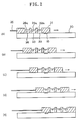
- the p-type GaAs substrate 10 is secured on a boat body 20 in such way that its top surface is flush with the top surface of the boat body 20.
- the first solution reservoir 22 which contains the p-type clad layer growth solution 22a, the second solution reservoir 23 which contains the p-type active layer growth solution 23a, and the third solution reservoir 24 which contains the n-type clad layer growth solution 24a are set up on the sliding solution reservoir 21.
- Each solution reservoir does not have a bottom, so that each solution directly soaks the top surface of the boat body 20.
- the sliding solution reservoir 21 is slidden, in the direction of the arrow, from the position indicated in Figure 2(a) to set the p-type clad layer growth solution 22a in the first reservoir 22 on the p-type GaAs substrate 10, and the p-type clad layer 11 is grown under the conditions where, for example, the temperature is lowered from 900°C to 800°C ( Figure 2(b)).
- the sliding solution reservoir 21 is slidden further in the direction of the arrow to set the p-type active layer growth solution 23a in the second reservoir 23 on the p-type GaAs substrate 10, and the p-type active layer is grown under the conditions where, for example, the temperature is lowered from 800°C to 795°C ( Figure 2(c)).
- the sliding solution reservoir 21 is then slidden further in the direction of the arrow to grow the n-type clad layer 13 under the conditions where, for example, the temperature is lowered from 795°C to 650°C ( Figure 2(d)).
- the sliding solution reservoir 21 is slidden further in the direction of the arrow to complete the growth process (Figure 2(e)).
- the amount of the p-type impurity Zn added to the p-type clad layer growth solution 22a is very small, or Zn is not added at all.
- the highly concentrated Zn added to the p-type GaAs substrate 10 diffuses into the clad layer, causing so-called "auto doping".
- the clad layer becomes the p-type clad layer 11 with the prescribed concentration profile, and an area with low carrier concentration (1 x 1016 cm ⁇ 3) is formed near the p-type active layer 12.
- the substrate is removed by etching and electrodes are formed on both sides of the three layer structure to obtain the light emitting device.
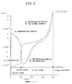
- Figure 3 shows a depth-wise carrier concentration profile of the light emitting device of this embodiment which was made as described above.
- the carrier concentration in the p-type clad layer 11 near the p-type GaAs substrate 10 is approximately equivalent to the carrier concentration in the substrate (1 to 3 x 1019 cm ⁇ 3).
- the carrier concentration in the p-type active layer is 1 x 1017 cm ⁇ 3.
- the carrier concentration in the n-clad layer 13 increases from 1 x 1017 cm ⁇ 3, which is equivalent to the carrier concentration in the p-type active layer, to approximately 6 x 1017 cm ⁇ 3 in the top region.
- Figure 4 shows the relationship between the carrier concentration in the p-type clad layer 11 near the p-type active layer 12 and the relative luminance of the light emitting device. It is shown that as the carrier concentration in the p-type clad layer 11 near the p-type active layer 12 decreases, the relative luminance of the light emitting device increases.
- Figure 5 shows the frequency distribution by relative luminance for the concentration range in the embodiment of this invention (1 to 2 x 1016 cm ⁇ 3) and the distribution for the conventional concentration range (1 to 2 x 1017 cm ⁇ 3). It is shown that the relative luminance for the concentration range in this embodiment (1 to 2 x 1016 cm ⁇ 3) is very high, approximately 400.
- a light emitting device comprising three layers, i.e., (a) a first clad layer composed of a mixed crystal compound semiconductor of first type conductivity, (b) an active layer composed of a mixed crystal compound semiconductor of second type conductivity which has the mixed crystal ratio required to emit the prescribed wavelength, and (c) a second clad layer composed of a mixed crystal compound semiconductor of second type conductivity which has a mixed crystal ratio equivalent to that of the first clad layer, wherein the active layer is sandwiched by the first and second clad layers and forms the double hetero structure with the first and second clad layers, it is possible to obtain higher luminance than that of conventional light emitting devices by keeping the carrier concentration in the first clad layer near the junction with the active layer at 5 x 1016 cm ⁇ 3 or less.
Landscapes
- Led Devices (AREA)
Applications Claiming Priority (2)
| Application Number | Priority Date | Filing Date | Title |
|---|---|---|---|
| JP157651/91 | 1991-05-31 | ||
| JP15765191 | 1991-05-31 |
Publications (2)
| Publication Number | Publication Date |
|---|---|
| EP0516162A1 true EP0516162A1 (fr) | 1992-12-02 |
| EP0516162B1 EP0516162B1 (fr) | 1995-12-27 |
Family
ID=15654389
Family Applications (1)
| Application Number | Title | Priority Date | Filing Date |
|---|---|---|---|
| EP92109119A Expired - Lifetime EP0516162B1 (fr) | 1991-05-31 | 1992-05-29 | Dispositif semi-conducteur émetteur de lumière |
Country Status (3)
| Country | Link |
|---|---|
| US (1) | US5323027A (fr) |
| EP (1) | EP0516162B1 (fr) |
| DE (1) | DE69207069T2 (fr) |
Cited By (1)
| Publication number | Priority date | Publication date | Assignee | Title |
|---|---|---|---|---|
| EP0704914A1 (fr) * | 1994-09-28 | 1996-04-03 | Shin-Etsu Handotai Company Limited | Dispositif émetteur de lumière |
Families Citing this family (6)
| Publication number | Priority date | Publication date | Assignee | Title |
|---|---|---|---|---|
| US5578839A (en) * | 1992-11-20 | 1996-11-26 | Nichia Chemical Industries, Ltd. | Light-emitting gallium nitride-based compound semiconductor device |
| US5442202A (en) * | 1993-10-29 | 1995-08-15 | Mitsubishi Cable Industries, Ltd. | Semiconductor light emitting element |
| US6996150B1 (en) | 1994-09-14 | 2006-02-07 | Rohm Co., Ltd. | Semiconductor light emitting device and manufacturing method therefor |
| JP3959434B2 (ja) * | 1995-08-29 | 2007-08-15 | 昭和電工株式会社 | 発光ダイオード素子 |
| US7184640B2 (en) * | 2004-02-25 | 2007-02-27 | Avago Technologies Fiber Ip (Singapore) Pte. Ltd. | Buried heterostructure device fabricated by single step MOCVD |
| US7440666B2 (en) * | 2004-02-25 | 2008-10-21 | Avago Technologies Fiber Ip (Singapore) Pte. Ltd. | Buried heterostucture device having integrated waveguide grating fabricated by single step MOCVD |
Citations (2)
| Publication number | Priority date | Publication date | Assignee | Title |
|---|---|---|---|---|
| EP0301893A2 (fr) * | 1987-07-31 | 1989-02-01 | Shin-Etsu Handotai Company, Limited | Dispositif semi-conducteur émetteur de lumière |
| EP0356037A2 (fr) * | 1988-08-26 | 1990-02-28 | Hewlett-Packard Company | Méthode de fabrication d'un dispositif électro-optique avec un substrat transparent inversé |
-
1992
- 1992-05-29 EP EP92109119A patent/EP0516162B1/fr not_active Expired - Lifetime
- 1992-05-29 US US07/889,372 patent/US5323027A/en not_active Expired - Fee Related
- 1992-05-29 DE DE69207069T patent/DE69207069T2/de not_active Expired - Fee Related
Patent Citations (2)
| Publication number | Priority date | Publication date | Assignee | Title |
|---|---|---|---|---|
| EP0301893A2 (fr) * | 1987-07-31 | 1989-02-01 | Shin-Etsu Handotai Company, Limited | Dispositif semi-conducteur émetteur de lumière |
| EP0356037A2 (fr) * | 1988-08-26 | 1990-02-28 | Hewlett-Packard Company | Méthode de fabrication d'un dispositif électro-optique avec un substrat transparent inversé |
Non-Patent Citations (1)
| Title |
|---|
| APPLIED PHYSICS LETTERS. vol. 50, no. 8, 23 February 1987, NEW YORK US pages 427 - 429; M. WATANABE ET AL.: 'optical tristability using a twin-stripe laser diode' * |
Cited By (2)
| Publication number | Priority date | Publication date | Assignee | Title |
|---|---|---|---|---|
| EP0704914A1 (fr) * | 1994-09-28 | 1996-04-03 | Shin-Etsu Handotai Company Limited | Dispositif émetteur de lumière |
| US5808324A (en) * | 1994-09-28 | 1998-09-15 | Shin-Etsu Handotai Co., Ltd | Light emitting device |
Also Published As
| Publication number | Publication date |
|---|---|
| DE69207069D1 (de) | 1996-02-08 |
| DE69207069T2 (de) | 1996-05-15 |
| EP0516162B1 (fr) | 1995-12-27 |
| US5323027A (en) | 1994-06-21 |
Similar Documents
| Publication | Publication Date | Title |
|---|---|---|
| JPH1154794A (ja) | 化合物半導体素子及びその製造方法 | |
| JPH05190898A (ja) | Led及びledの形成方法 | |
| JP2708165B2 (ja) | 半導体構造およびその製造方法 | |
| CA1049127A (fr) | Dispositifs a semiconducteur avec rayonnement thermique et concentration de courant ameliores | |
| EP0516162B1 (fr) | Dispositif semi-conducteur émetteur de lumière | |
| JP2681352B2 (ja) | 発光半導体素子 | |
| JP2781097B2 (ja) | 半導体装置およびその製造方法 | |
| JP2795195B2 (ja) | 発光素子 | |
| JP4233570B2 (ja) | 半導体材料およびこれを用いた半導体素子 | |
| JPH09129927A (ja) | 青色発光素子 | |
| JPH0691280B2 (ja) | 半導体発光ダイオード | |
| KR19980070852A (ko) | 에피택시얼 웨이퍼 및 이의 제조방법과 휘도가 증가된 발광다이오드 | |
| JPS6244717B2 (fr) | ||
| JP2681431B2 (ja) | 発光素子 | |
| US5585305A (en) | Method for fabricating a semiconductor device | |
| EP0529554A1 (fr) | Méthode pour la fabrication d'un dispositif semi-conducteur | |
| JP4156873B2 (ja) | エピタキシャルウエハの製造方法 | |
| JPH08293622A (ja) | 赤外発光ダイオードおよびその製造方法 | |
| JPS63213378A (ja) | 半導体発光素子の製造方法 | |
| JPH04260386A (ja) | 光半導体装置の製造方法 | |
| JP4319291B2 (ja) | 半導体発光素子用エピタキシャル基板及び発光素子 | |
| JP2002261321A (ja) | 半導体発光装置 | |
| JPH0351674B2 (fr) | ||
| JP2783580B2 (ja) | ダブルヘテロ型赤外光発光素子 | |
| JPH07211660A (ja) | GaAlAs系LED用エピタキシャルウェハ及びその製造方法 |
Legal Events
| Date | Code | Title | Description |
|---|---|---|---|
| PUAI | Public reference made under article 153(3) epc to a published international application that has entered the european phase |
Free format text: ORIGINAL CODE: 0009012 |
|
| AK | Designated contracting states |
Kind code of ref document: A1 Designated state(s): DE FR GB |
|
| 17P | Request for examination filed |
Effective date: 19930130 |
|
| 17Q | First examination report despatched |
Effective date: 19940705 |
|
| GRAA | (expected) grant |
Free format text: ORIGINAL CODE: 0009210 |
|
| AK | Designated contracting states |
Kind code of ref document: B1 Designated state(s): DE FR GB |
|
| REF | Corresponds to: |
Ref document number: 69207069 Country of ref document: DE Date of ref document: 19960208 |
|
| ET | Fr: translation filed | ||
| PLBE | No opposition filed within time limit |
Free format text: ORIGINAL CODE: 0009261 |
|
| STAA | Information on the status of an ep patent application or granted ep patent |
Free format text: STATUS: NO OPPOSITION FILED WITHIN TIME LIMIT |
|
| 26N | No opposition filed | ||
| PGFP | Annual fee paid to national office [announced via postgrant information from national office to epo] |
Ref country code: FR Payment date: 19990511 Year of fee payment: 8 |
|
| PGFP | Annual fee paid to national office [announced via postgrant information from national office to epo] |
Ref country code: GB Payment date: 19990526 Year of fee payment: 8 |
|
| PG25 | Lapsed in a contracting state [announced via postgrant information from national office to epo] |
Ref country code: GB Free format text: LAPSE BECAUSE OF NON-PAYMENT OF DUE FEES Effective date: 20000529 |
|
| GBPC | Gb: european patent ceased through non-payment of renewal fee |
Effective date: 20000529 |
|
| PG25 | Lapsed in a contracting state [announced via postgrant information from national office to epo] |
Ref country code: FR Free format text: LAPSE BECAUSE OF NON-PAYMENT OF DUE FEES Effective date: 20010131 |
|
| REG | Reference to a national code |
Ref country code: FR Ref legal event code: ST |
|
| PGFP | Annual fee paid to national office [announced via postgrant information from national office to epo] |
Ref country code: DE Payment date: 20030605 Year of fee payment: 12 |
|
| PG25 | Lapsed in a contracting state [announced via postgrant information from national office to epo] |
Ref country code: DE Free format text: LAPSE BECAUSE OF NON-PAYMENT OF DUE FEES Effective date: 20041201 |