EP0518667A1 - Connecteur traversant une plaque montée en surface - Google Patents
Connecteur traversant une plaque montée en surface Download PDFInfo
- Publication number
- EP0518667A1 EP0518667A1 EP92305370A EP92305370A EP0518667A1 EP 0518667 A1 EP0518667 A1 EP 0518667A1 EP 92305370 A EP92305370 A EP 92305370A EP 92305370 A EP92305370 A EP 92305370A EP 0518667 A1 EP0518667 A1 EP 0518667A1
- Authority
- EP
- European Patent Office
- Prior art keywords
- connector
- contacts
- circuits
- portions
- printed circuit
- Prior art date
- Legal status (The legal status is an assumption and is not a legal conclusion. Google has not performed a legal analysis and makes no representation as to the accuracy of the status listed.)
- Granted
Links
- 230000013011 mating Effects 0.000 claims description 9
- 229910000679 solder Inorganic materials 0.000 claims description 8
- 238000000034 method Methods 0.000 claims description 7
- 238000005476 soldering Methods 0.000 claims description 5
- 239000002184 metal Substances 0.000 claims description 3
- 229920003023 plastic Polymers 0.000 abstract description 3
- 238000004806 packaging method and process Methods 0.000 description 4
- 239000006071 cream Substances 0.000 description 3
- ATJFFYVFTNAWJD-UHFFFAOYSA-N Tin Chemical compound [Sn] ATJFFYVFTNAWJD-UHFFFAOYSA-N 0.000 description 1
- 238000010276 construction Methods 0.000 description 1
- 229920006351 engineering plastic Polymers 0.000 description 1
- 238000005516 engineering process Methods 0.000 description 1
- 230000004907 flux Effects 0.000 description 1
- 239000011888 foil Substances 0.000 description 1
- LQBJWKCYZGMFEV-UHFFFAOYSA-N lead tin Chemical compound [Sn].[Pb] LQBJWKCYZGMFEV-UHFFFAOYSA-N 0.000 description 1
- 239000000463 material Substances 0.000 description 1
- 230000000284 resting effect Effects 0.000 description 1
Images

Classifications
-
- H—ELECTRICITY
- H01—ELECTRIC ELEMENTS
- H01R—ELECTRICALLY-CONDUCTIVE CONNECTIONS; STRUCTURAL ASSOCIATIONS OF A PLURALITY OF MUTUALLY-INSULATED ELECTRICAL CONNECTING ELEMENTS; COUPLING DEVICES; CURRENT COLLECTORS
- H01R12/00—Structural associations of a plurality of mutually-insulated electrical connecting elements, specially adapted for printed circuits, e.g. printed circuit boards [PCB], flat or ribbon cables, or like generally planar structures, e.g. terminal strips, terminal blocks; Coupling devices specially adapted for printed circuits, flat or ribbon cables, or like generally planar structures; Terminals specially adapted for contact with, or insertion into, printed circuits, flat or ribbon cables, or like generally planar structures
- H01R12/70—Coupling devices
- H01R12/71—Coupling devices for rigid printing circuits or like structures
- H01R12/712—Coupling devices for rigid printing circuits or like structures co-operating with the surface of the printed circuit or with a coupling device exclusively provided on the surface of the printed circuit
- H01R12/716—Coupling device provided on the PCB
Definitions
- This invention relates to an electrical connector of a type adapted to extend through a printed circuit board and be interconnected to circuits on the lower surface of such board.
- SMT Surface mount technology
- U.S. patent No. 4,917,614 discloses such an SMT connector.
- SMT contrasts with earlier developed techniques wherein printed circuit boards contained holes with connectors and components having contacts with pins that were fitted in such holes with soldering to the printed circuit board occurring either on the bottom or within the holes by a suitable solder reflow.
- component and connector contacts are coated with a tin or tin lead material, compatible with the use of solder creams and/or reflowable in and of itself.
- weight and volume become important, and the overall height and volume of aninstalled component and/or connector and a printed circuit board can become critical.
- an object of the present invention to provide an electrical connector for use with a printed circuit board that allows a use of SMT with a reduced height and volume of the connector and printed circuit board for improved packaging. It is still a further object to provide an electrical connector having a housing and contacts oriented to maximize center-to-center spacing, and at the same time, facilitate soldering of such contacts to conventionally oriented circuit traces on printed circuit boards.
- the present invention achieves the foregoing objectives through the provision of an electrical connector having a plastic housing containing electrical contacts therein with the housing and contacts having a configuration to fit through an aperture in a printed circuit board and extend above and beneath the board upper and lower surfaces.
- the contacts include first portions oriented perpendicularly to the board surface and adapted to interconnect with the contacts of a mating connector and second portions that extend generally in a plane parallel to that of the printed circuit board with upper surfaces that engage circuits carried on the lower surface of the board. In this way, the overall height of board and connector is reduced by the thickness of the board through which the connector housing is fitted.
- the contacts of the invention connector are stamped and formed of thin, flat metal stock, preferably of a spring grade and hardness to allow for the provision of a resilient contact, provided in the upper portion of the contact.
- the upper portions of the contacts are formed to extend in a row or rows and parallel to an axis oblique to the length axis of the housing. This facilitates an improvement in density of contacts facing by reducing the effective width of the contacts in the housing.
- the contacts each include lower portions that extend at right angles to the length axis of the housing so as to be conventionally oriented relative to standard X and Y patterns of pads and traces on printed circuit boards. Contacts are set on edge to further minimize the allowable center-to-center spacing of such contacts in such housing.
- the upper surfaces of the second portions of the contacts are rounded to facilitate soldering to circuits on the underside surface of the printed circuit board.
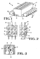
- Figure 1 is a perspective view of an electrical connector in accordance with the invention.
- Figure 2 is a partial plan view of the connector shown in Figure 1.
- Figure 3 is a side view taken through lines 3-3 of Figure 2.
- Figure 4 is a side, elevational view of a contact of the invention.
- Figure 5 is a plan view of a printed circuit board from the underside, showing circuits thereon and an aperture therein.
- Figure 6 is a side, elevational, and partially sectioned view showing the connector of the invention installed in a printed circuit board aperture.
- an electrical connector 10 of the SMT variety is shown to include a plastic housing 12 that has an upper portion 13 and a lower portion 14 in the form of wings that extend transversely of the housing 12.
- the mating axis with connector 10 is parallel to the height of the housing and transverse to the extension of projections 14.
- a mating connector, not shown, would be utilized to engage connector 10 and interconnect such connector to further circuits such as printed circuit boards or flexible circuits, or wires and cables.
- Housing 12 would typically be molded of an engineering plastic having suitable dielectric quality characteristics.
- Housing 12 includes, as is shown in Figure 2, a series of apertures 16 that extend through the height of the housing.
- the contacts 20, as shown in Figures 2 and 3, are bifurcated to include a U-shaped portion 22 having interiorly rounded surfaces 21, shown in Figure 4, with the surfaces 21 engaging post or pins of mating connectors and the arms 22 operating to provide a normal spring force adequate to ensure a low-resistance, stable electrical interface with such mating pin portions.
- the contacts 20 include a projection 23 that projects sideways to latch or lock the contacts within the housing by engaging internal surfaces of the housing not shown.
- the contacts have a base portion 24 and a narrowed neck portion 25 joining the upper portion 22.
- the neck portion 25 serves to facilitate slight movements caused by tolerance variations with respect to the contacts 20 and mating contacts.
- Extending from the base portion 24 is a lower contact portion 26 having a rounded upper surface 28, the portion 26 extending out from base portion at an angle in the manner shown in Figure 2 relative to upper portion 22.
- portions 26 extend through slots 15 in the wing portions 14 of housing 12. As can be seen from Figure 1, portions 26 extend above the projecting portions 14 of housing 12 so that rounded, or tapered, surfaces 28 extend in a parallel plane.
- a printed circuit board 30 is shown to include an aperture 32 extending therethrough with circuit pads 34 extended on the lower surface of the board 30, note Figure 6, outward from the edge surfaces of aperture 32.
- the cross-sectional profile of housing 12 of the connector is shown in phantom in Figure 5.
- pads 34 are to be understood to be connected to further circuit traces within board 30 or on the opposite sides thereof that extend to interconnect to components or other connectors or the like.
- the orientation of pads 34 transverse to the length axis of aperture 32 and therefore to the length axis of housing 12 as mounted within the aperture.
- the provision of the bulk of circuit traces and pads on printed circuit boards along conventional X and Y axes is thus accommodated by the arrangement of traces as shown in Figure 5.
- portions 26, oriented in a conventional manner, transverse to the length axis of the housing 12 and to the length axis of the aperture 32.
- the contacts 20, the upper portions thereof are oriented obliquely to such axis. This facilitates a stacking in side-by-side relationship that accommodates a closer center-to-center spacing, both in a sense relative to the width of the housing 12 or in relation to the length of the housing.
- the printed circuit board 30 includes an upper surface 31 and a lower surface 33 interconnected by aperture 32 with circuit pads 34 formed on the undersurface 33.
- Connector 10 is made to fit within the aperture, the upper portion 13 extending up through the aperture above the surface 31 and wing portions 14 carrying portions 26 of the contacts extending beneath the surface 33 to allow the upper surfaces 28 to engage pads 34 and be soldered thereto by a reflowing of solder cream applied either to the contacts or to the pads.
- Fastening means can be used to secure the connector to the circuit board prior to soldering contact portions 26 to pads 34, if desired.
- the invention contemplates an alternative potential use of the connector of the invention by extending the contact portions 26 below or beneath the portions 14.
- the connector 10 could be placed on the top surface of board 30 and soldered thereto with the contact portions 26 resting on such surface and on pads thereon.
- the same connector could be employed in certain areas on printed circuit boards to minimize overall package height and in other areas, placed on top of the board for configuration considerations; as for example, along an edge of the board to provide an I/O function.
- the bottom surfaces of portions 26 would be preferably rounded.
- the present invention thus provides an SMT connector that takes advantage of height by extending through the thickness of the board to reduce the overall packaging height required and through the provision of the contacts, and orientation thereof maximizes a density of contacts in terms of center-to-center spacing.
Landscapes
- Coupling Device And Connection With Printed Circuit (AREA)
- Multi-Conductor Connections (AREA)
Applications Claiming Priority (2)
| Application Number | Priority Date | Filing Date | Title |
|---|---|---|---|
| JP53173/91U | 1991-06-14 | ||
| JP1991053173U JP2555593Y2 (ja) | 1991-06-14 | 1991-06-14 | 表面実装型コネクタ |
Publications (2)
| Publication Number | Publication Date |
|---|---|
| EP0518667A1 true EP0518667A1 (fr) | 1992-12-16 |
| EP0518667B1 EP0518667B1 (fr) | 1996-10-23 |
Family
ID=12935471
Family Applications (1)
| Application Number | Title | Priority Date | Filing Date |
|---|---|---|---|
| EP92305370A Expired - Lifetime EP0518667B1 (fr) | 1991-06-14 | 1992-06-11 | Connecteur traversant une plaque montée en surface |
Country Status (4)
| Country | Link |
|---|---|
| US (1) | US5197891A (fr) |
| EP (1) | EP0518667B1 (fr) |
| JP (1) | JP2555593Y2 (fr) |
| DE (1) | DE69214727T2 (fr) |
Cited By (2)
| Publication number | Priority date | Publication date | Assignee | Title |
|---|---|---|---|---|
| ES2383746A1 (es) * | 2004-05-14 | 2012-06-26 | Tyco Electronics Japan G.K. | Conector electrico montado en placa |
| EP2139079B1 (fr) * | 2008-06-23 | 2016-03-23 | Tyco Electronics Corporation | Connecteur inversé traversant la carte |
Families Citing this family (26)
| Publication number | Priority date | Publication date | Assignee | Title |
|---|---|---|---|---|
| US5685726A (en) * | 1992-07-17 | 1997-11-11 | Berg Technology, Inc. | Flat back card connector |
| DE69326613T2 (de) * | 1992-07-17 | 2004-08-26 | Berg Electronics Manufacturing B.V. | Kartenverbinder mit flacher rückseite |
| US5713744A (en) * | 1994-09-28 | 1998-02-03 | The Whitaker Corporation | Integrated circuit socket for ball grid array and land grid array lead styles |
| US5525072A (en) * | 1995-01-10 | 1996-06-11 | Molex Incorporated | Electrical connector assembly for interconnecting a flat cable to a circuit board |
| US5938456A (en) * | 1995-04-19 | 1999-08-17 | Methode Electronics, Inc. | Low profile electrical connector |
| US6172590B1 (en) | 1996-01-22 | 2001-01-09 | Surgx Corporation | Over-voltage protection device and method for making same |
| US6013358A (en) * | 1997-11-18 | 2000-01-11 | Cooper Industries, Inc. | Transient voltage protection device with ceramic substrate |
| US5960537A (en) * | 1998-02-02 | 1999-10-05 | Samtec, Inc. | Fastener for an electrical connector |
| US6064094A (en) * | 1998-03-10 | 2000-05-16 | Oryx Technology Corporation | Over-voltage protection system for integrated circuits using the bonding pads and passivation layer |
| US6126489A (en) * | 1998-10-30 | 2000-10-03 | The Whitaker Corporation | Electrical connector for printed circuit boards |
| JP2000251989A (ja) * | 1999-03-01 | 2000-09-14 | Yazaki Corp | コネクタの基板接続構造及び基板接続方法 |
| US6373719B1 (en) | 2000-04-13 | 2002-04-16 | Surgx Corporation | Over-voltage protection for electronic circuits |
| JP3411904B2 (ja) * | 2000-12-25 | 2003-06-03 | 山一電機株式会社 | 実装コネクタおよびコンタクト端子 |
| US20060258192A1 (en) * | 2005-05-11 | 2006-11-16 | Hon Hai Precision Ind. Co., Ltd. | Bottom PCB surface mount electrical connector |
| JP4248555B2 (ja) * | 2006-02-21 | 2009-04-02 | 日本航空電子工業株式会社 | コネクタ |
| TWM340654U (en) * | 2008-01-07 | 2008-09-11 | Hon Hai Prec Ind Co Ltd | Electrical connector |
| US7850466B2 (en) * | 2008-06-23 | 2010-12-14 | Tyco Electronics Corporation | Through board inverted connector |
| CN101420089B (zh) * | 2008-12-01 | 2013-03-06 | 友达光电(厦门)有限公司 | 电子装置及其连接器固定结构 |
| US7892031B1 (en) * | 2009-07-30 | 2011-02-22 | Tyco Electronics Corporation | Quick insertion lamp assembly |
| CN201667411U (zh) * | 2010-03-31 | 2010-12-08 | 富士康(昆山)电脑接插件有限公司 | 电连接器 |
| JP5051796B2 (ja) * | 2010-04-20 | 2012-10-17 | 日本航空電子工業株式会社 | コネクタ |
| CN201797194U (zh) | 2010-05-18 | 2011-04-13 | 富士康(昆山)电脑接插件有限公司 | 电连接器及其组件 |
| JP2013122877A (ja) * | 2011-12-12 | 2013-06-20 | Tyco Electronics Japan Kk | コネクタ |
| DE102014102845A1 (de) * | 2014-03-04 | 2015-09-10 | Phoenix Contact Gmbh & Co. Kg | Elektrischer Klemmenblock |
| CN204696277U (zh) * | 2015-04-27 | 2015-10-07 | 富士康(昆山)电脑接插件有限公司 | 连接器及其组合 |
| CN205039288U (zh) * | 2015-08-27 | 2016-02-17 | 泰科电子(上海)有限公司 | 连接器 |
Citations (2)
| Publication number | Priority date | Publication date | Assignee | Title |
|---|---|---|---|---|
| GB2022337A (en) * | 1978-06-02 | 1979-12-12 | Nissan Motor | Electrical connector assenbly |
| US4750889A (en) * | 1987-02-27 | 1988-06-14 | Minnesota Mining & Manufacturing Company | Through-board electrical component header having integral solder mask |
Family Cites Families (8)
| Publication number | Priority date | Publication date | Assignee | Title |
|---|---|---|---|---|
| EP0404277B1 (fr) * | 1984-02-27 | 1994-09-28 | The Whitaker Corporation | Méthode d'insertion d'un contact de support de puce dans un boîtier |
| US4917614A (en) * | 1987-05-12 | 1990-04-17 | Amp Incorporated | Electrical connector for surface mounting onto circuit boards |
| JPH0290481A (ja) * | 1988-09-27 | 1990-03-29 | Matsushita Electric Works Ltd | コネクタ装置 |
| US4948030A (en) * | 1989-01-30 | 1990-08-14 | Motorola, Inc. | Bond connection for components |
| JPH0344995A (ja) * | 1989-07-12 | 1991-02-26 | Toshiba Corp | プリント配線基板 |
| JP2885379B2 (ja) * | 1989-08-23 | 1999-04-19 | 富士写真光機 株式会社 | テレビカメラ操作装置 |
| US5030107A (en) * | 1990-11-08 | 1991-07-09 | Molex Incorporated | LCD cluster connector |
| KR200214890Y1 (ko) * | 2000-09-01 | 2001-02-15 | 주식회사한국할로겐 | 할로겐 히터장치 |
-
1991
- 1991-06-14 JP JP1991053173U patent/JP2555593Y2/ja not_active Expired - Fee Related
-
1992
- 1992-05-15 US US07/884,092 patent/US5197891A/en not_active Expired - Fee Related
- 1992-06-11 DE DE69214727T patent/DE69214727T2/de not_active Expired - Fee Related
- 1992-06-11 EP EP92305370A patent/EP0518667B1/fr not_active Expired - Lifetime
Patent Citations (2)
| Publication number | Priority date | Publication date | Assignee | Title |
|---|---|---|---|---|
| GB2022337A (en) * | 1978-06-02 | 1979-12-12 | Nissan Motor | Electrical connector assenbly |
| US4750889A (en) * | 1987-02-27 | 1988-06-14 | Minnesota Mining & Manufacturing Company | Through-board electrical component header having integral solder mask |
Non-Patent Citations (1)
| Title |
|---|
| RESEARCH DISCLOSURE no. 269, September 1986, HAVANT GB page 516 ANONYM '26902 Molded Stackable Surface Mounted Connector' * |
Cited By (2)
| Publication number | Priority date | Publication date | Assignee | Title |
|---|---|---|---|---|
| ES2383746A1 (es) * | 2004-05-14 | 2012-06-26 | Tyco Electronics Japan G.K. | Conector electrico montado en placa |
| EP2139079B1 (fr) * | 2008-06-23 | 2016-03-23 | Tyco Electronics Corporation | Connecteur inversé traversant la carte |
Also Published As
| Publication number | Publication date |
|---|---|
| JPH04136876U (ja) | 1992-12-21 |
| JP2555593Y2 (ja) | 1997-11-26 |
| US5197891A (en) | 1993-03-30 |
| EP0518667B1 (fr) | 1996-10-23 |
| DE69214727T2 (de) | 1997-05-07 |
| DE69214727D1 (de) | 1996-11-28 |
Similar Documents
| Publication | Publication Date | Title |
|---|---|---|
| EP0518667A1 (fr) | Connecteur traversant une plaque montée en surface | |
| CA2267292C (fr) | Connecteur extra-plat | |
| US5709574A (en) | Surface-mountable socket connector | |
| US7931477B2 (en) | Low profile board-to-board connector mating pair with solder barrier | |
| US6241535B1 (en) | Low profile connector | |
| KR100432860B1 (ko) | 전자 패키지용 표면장착 소켓 및 이와 함께 사용되는 컨택트 | |
| US4679889A (en) | Solder-bearing leads | |
| EP0706240A1 (fr) | Connecteurs électriques entre deux plaquettes à circuits imprimés | |
| JPH10284194A (ja) | 一体化されたpcbアセンブリを有する表面実装コネクタ | |
| EP0017358B1 (fr) | Boîtier de connecteur électrique avec un plot d'enfischage | |
| KR950702752A (ko) | 배면 납작형 카드 커넥터(Flat Back Card Connector) | |
| JPH11514131A (ja) | 応力を分離したはんだテールを有する電気コネクタ | |
| US6135784A (en) | LIF PGA socket | |
| GB2242579A (en) | Electrical connectors for flat insulated boards | |
| JPH0668940A (ja) | Fpc接続用コネクタ | |
| JPH07211370A (ja) | プリント回路基板取付型電気コネクタ | |
| EP0299989B1 (fr) | Prise pour plaquette de circuit a haute densite | |
| US5407360A (en) | Connector for high density electronic assemblies | |
| US6769924B1 (en) | Electrical connector having a releasable cover | |
| JPH0617164U (ja) | 平板状接続部材のコネクタ装置 | |
| JPH0617165U (ja) | 平板状接続部材のコネクタ装置 | |
| KR930002845Y1 (ko) | 콘넥터 구조 | |
| JPH0611283U (ja) | カードコネクタ | |
| JP3342585B2 (ja) | Fpcコネクタのテーピング方法 | |
| KR100647154B1 (ko) | 전기 커넥터 |
Legal Events
| Date | Code | Title | Description |
|---|---|---|---|
| PUAI | Public reference made under article 153(3) epc to a published international application that has entered the european phase |
Free format text: ORIGINAL CODE: 0009012 |
|
| AK | Designated contracting states |
Kind code of ref document: A1 Designated state(s): DE FR GB |
|
| RAP1 | Party data changed (applicant data changed or rights of an application transferred) |
Owner name: THE WHITAKER CORPORATION |
|
| 17P | Request for examination filed |
Effective date: 19930513 |
|
| 17Q | First examination report despatched |
Effective date: 19941209 |
|
| GRAH | Despatch of communication of intention to grant a patent |
Free format text: ORIGINAL CODE: EPIDOS IGRA |
|
| GRAH | Despatch of communication of intention to grant a patent |
Free format text: ORIGINAL CODE: EPIDOS IGRA |
|
| GRAA | (expected) grant |
Free format text: ORIGINAL CODE: 0009210 |
|
| AK | Designated contracting states |
Kind code of ref document: B1 Designated state(s): DE FR GB |
|
| REF | Corresponds to: |
Ref document number: 69214727 Country of ref document: DE Date of ref document: 19961128 |
|
| ET | Fr: translation filed | ||
| PLBE | No opposition filed within time limit |
Free format text: ORIGINAL CODE: 0009261 |
|
| STAA | Information on the status of an ep patent application or granted ep patent |
Free format text: STATUS: NO OPPOSITION FILED WITHIN TIME LIMIT |
|
| 26N | No opposition filed | ||
| PGFP | Annual fee paid to national office [announced via postgrant information from national office to epo] |
Ref country code: GB Payment date: 19990504 Year of fee payment: 8 |
|
| PGFP | Annual fee paid to national office [announced via postgrant information from national office to epo] |
Ref country code: FR Payment date: 19990602 Year of fee payment: 8 |
|
| PG25 | Lapsed in a contracting state [announced via postgrant information from national office to epo] |
Ref country code: GB Free format text: LAPSE BECAUSE OF NON-PAYMENT OF DUE FEES Effective date: 20000611 |
|
| GBPC | Gb: european patent ceased through non-payment of renewal fee |
Effective date: 20000611 |
|
| PG25 | Lapsed in a contracting state [announced via postgrant information from national office to epo] |
Ref country code: FR Free format text: LAPSE BECAUSE OF NON-PAYMENT OF DUE FEES Effective date: 20010228 |
|
| REG | Reference to a national code |
Ref country code: FR Ref legal event code: ST |
|
| PGFP | Annual fee paid to national office [announced via postgrant information from national office to epo] |
Ref country code: DE Payment date: 20010627 Year of fee payment: 10 |
|
| PG25 | Lapsed in a contracting state [announced via postgrant information from national office to epo] |
Ref country code: DE Free format text: LAPSE BECAUSE OF NON-PAYMENT OF DUE FEES Effective date: 20030101 |