EP0519739A1 - Impulsflanke integrierender Phasendetektor - Google Patents
Impulsflanke integrierender Phasendetektor Download PDFInfo
- Publication number
- EP0519739A1 EP0519739A1 EP92305650A EP92305650A EP0519739A1 EP 0519739 A1 EP0519739 A1 EP 0519739A1 EP 92305650 A EP92305650 A EP 92305650A EP 92305650 A EP92305650 A EP 92305650A EP 0519739 A1 EP0519739 A1 EP 0519739A1
- Authority
- EP
- European Patent Office
- Prior art keywords
- signal
- edge
- sync
- locked loop
- phase locked
- Prior art date
- Legal status (The legal status is an assumption and is not a legal conclusion. Google has not performed a legal analysis and makes no representation as to the accuracy of the status listed.)
- Granted
Links
- 230000007704 transition Effects 0.000 claims description 9
- 238000005070 sampling Methods 0.000 claims description 7
- 230000003252 repetitive effect Effects 0.000 claims description 6
- 238000010586 diagram Methods 0.000 description 4
- 230000000694 effects Effects 0.000 description 3
- 230000010354 integration Effects 0.000 description 1
- 230000000630 rising effect Effects 0.000 description 1
Images

Classifications
-
- H—ELECTRICITY
- H03—ELECTRONIC CIRCUITRY
- H03L—AUTOMATIC CONTROL, STARTING, SYNCHRONISATION OR STABILISATION OF GENERATORS OF ELECTRONIC OSCILLATIONS OR PULSES
- H03L7/00—Automatic control of frequency or phase; Synchronisation
- H03L7/06—Automatic control of frequency or phase; Synchronisation using a reference signal applied to a frequency- or phase-locked loop
- H03L7/08—Details of the phase-locked loop
- H03L7/085—Details of the phase-locked loop concerning mainly the frequency- or phase-detection arrangement including the filtering or amplification of its output signal
- H03L7/091—Details of the phase-locked loop concerning mainly the frequency- or phase-detection arrangement including the filtering or amplification of its output signal the phase or frequency detector using a sampling device
Definitions
- the present invention relates to phase locked loops, and more particularly to an edge integrating phase detector for a phase lock loop that acts to minimize jitter due to noise of a timing system derived from an input signal while maintaining a relatively large bandwidth in the system to respond to timing variations in the input signal.
- a video waveform has a repetitive reference component, referred to as sync, that is used to generate timing for the system. To generate this timing it is necessary to lock a local oscillator to the sync component so that all processing within the system occurs at known timing relationships with the video waveform.
- a phase locked loop is used that compares the phase of a reference clock to a sync signal derived from the sync component and adjusts the frequency of the reference clock until the phase between the two signals has a predetermined value.
- the video waveform is input to a sync stripper that provides the derived sync signal as a train of pulses, each pulse having a leading edge corresponding to a timing reference point on the video waveform.
- the sync stripper compares the video waveform with a fixed level, with the leading edges of the pulses in the derived sync signal occurring when the video waveform level crosses the fixed level in a given direction. Noise in the video waveform causes this crossing point to vary on a random basis, producing jitter in the derived sync signal.
- the derived sync signal is input to a phase detector together with a clock signal derived from the video system clock.
- the difference in phase between the appropriate clock signal edge and the corresponding sync signal edge is converted into an error voltage that is applied to the system clock to adjust its frequency until the phase difference achieves the predetermined value. If there is noise on the video waveform that causes jitter in the derived sync signal, as described above the period between the pulses of the derived sync signal vary, and there is a constant correcting of the system clock such that the phase locked loop output has jitter relative to the input signal.
- a loop filter having a very low bandwidth is inserted into the phase locked loop so that only an average variation in the period between pulses affects the timing of the phase locked loop.
- the low bandwidth loop filter while effectively reducing jitter, reduces the response time to variations in the reference sync signal.
- phase locked loop that reduces jitter due to noise on a video waveform while maintaining the ability to respond rapidly to variations in the video waveform.
- the present invention provides an edge integrating phase detector for a phase lock loop that reduces jitter due to noise on an input video waveform by integrating an edge of a sync pulse contained within the video waveform.
- the input video waveform is buffered and input to a gated sampling circuit that passes the edge, or transition, of the sync pulse to an integrating circuit.
- a gate signal for the gated sampling circuit is derived from a system clock.
- the output of the integrating circuit is input to an error amplifier together with a reference signal that represents the timing reference level of the sync pulse to produce an error signal that is fed back to control the frequency of the system clock, and thus the position of the gate signal relative to the sync pulse edge.
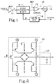
- Fig. 1 is a block diagram of a phase locked loop incorporating an edge integrating phase detector according to the present invention.
- Fig. 2 is a simplified schematic diagram of the edge integrating phase detector according to the present invention.
- Fig. 3 is a simplified block diagram of a gate generator for the edge integrating phase detector according to the present invention.
- Fig. 4 is a timing diagram for the phase locked loop incorporating the edge integrating phase detector according to the present invention.
- a phase locked loop 10 having a voltage controlled oscillator (VCO) 12 that provides a system clock signal CLOCK .
- VCO voltage controlled oscillator
- the gate strobe signal B is produced by a gate generator 18 that receives as an input the clock signal.
- the input signal is integrated by the edge integrating phase detector 16 during the gate strobe signal B .
- the integrated result from the edge integrating phase detector 16 is input as an essentially d.c.
- the d.c. signal is compared in the error amplifier 20 with a reference voltage REF that corresponds to the appropriate voltage level for the timing reference point of the input signal.
- REF reference voltage
- the voltage level for the sync point is ground, while for an NTSC video signal the voltage level for the sync point is -20 IRE.
- the output of the error amplifier 20 is an error signal that is applied to the VCO 12 to adjust the frequency of the VCO.
- the integration of the sync edge essentially removes jitter due to noise so that the loop filter of the error amplifier 20 may have a higher bandwidth, i.e., on the order of 50 times higher, than prior art loop filters.
- the gate strobe signal B is input to a sampling circuit 22 . Also input to the sampling circuit 22 is the input signal A . At the output C of the sampling circuit 22 the portion of the input signal A captured during the gate strobe signal B is passed to an integrating circuit 24 . Any suitable integrating circuit may be used, and in its most simplistic form is an RC circuit as shown. The integrating circuit 24 integrates about the sync point so that there is a negative and positive portion at the input.
- the gate strobe signal B is centered about the sync point, and the output of the integrating circuit 24 is at the reference level so that the output of the error amplifier 20 does not change the VCO 12 frequency.
- the gate strobe signal generator 18 is shown in Fig. 3 as having a counter 26 and a decoder 28 .
- the counter 26 counts the pulses of the clock signal CLOCK from the VCO 12 .
- the count from the counter 26 is input to the decoder 28 that provides the leading edge of the gate strobe signal B when the count reaches a predetermined value that is a function of the format of the input signal. If the phase locked loop 10 is locked, then the leading edge of the gate strobe signal B occurs shortly after the start of the transition of the sync edge from one level to another.
- the decoder 28 holds the gate strobe signal B for a range of counts from the counter 26 corresponding to a predetermined number of pulses of the clock signal CLOCK .
- an HDTV video signal A has a tri-level sync pattern with the sync point X occurring at the middle of the rising transition.
- the gate strobe signal B turns on the sampling circuit 22 and allows a portion C of the sync signal to drive the integrating circuit 24 .
- the gate strobe signal B is late so that the integrating circuit 24 receives unequal positive and negative inputs.
- the output of the integrating circuit 24 is proportional to the input unbalance, and thus through the error amplifier 20 drives the VCO 12 to correct the gate strobe signal timing. Noise that occurs within the gate strobe period is integrated and has little effect on the timing of the phase locked loop 10 .
- the VCO 12 may have a range of frequencies between 68-78 MHz.
- the rise time of the sync edge of the HDTV video signal is approximately 50 ns, while the fall time of the sync edge of an NTSC video signal is approximately 140 ns.
- the strobe width of the gate strobe signal B preferably is less than the transition times of the sync edges, i.e., strobe widths of 40 ns for HDTV and 110 ns for NTSC, but it may be longer so long as The width is substantially filled by the transition so that the error signal is essentially the integral of the sync edge transition.
- a variable delay circuit such as that described in Research Disclosure August 1990, pages 633-634, may be inserted in the gate strobe signal path to provide more precise timing for varying the phase of the system clock CLOCK relative to the input signal.
- the present invention provides an edge integrating phase detector for a phase locked loop that integrates the transition of a repetitive component in an input signal in order to generate an error signal for controlling the phase of a clock oscillator relative to the repetitive component while minimizing the effect of noise on the phase locked loop.
Landscapes
- Synchronizing For Television (AREA)
- Stabilization Of Oscillater, Synchronisation, Frequency Synthesizers (AREA)
- Television Signal Processing For Recording (AREA)
Applications Claiming Priority (2)
| Application Number | Priority Date | Filing Date | Title |
|---|---|---|---|
| US71744091A | 1991-06-19 | 1991-06-19 | |
| US717440 | 2000-11-21 |
Publications (2)
| Publication Number | Publication Date |
|---|---|
| EP0519739A1 true EP0519739A1 (de) | 1992-12-23 |
| EP0519739B1 EP0519739B1 (de) | 1997-10-01 |
Family
ID=24882048
Family Applications (1)
| Application Number | Title | Priority Date | Filing Date |
|---|---|---|---|
| EP19920305650 Expired - Lifetime EP0519739B1 (de) | 1991-06-19 | 1992-06-19 | Impulsflanke integrierender Phasendetektor |
Country Status (4)
| Country | Link |
|---|---|
| EP (1) | EP0519739B1 (de) |
| JP (1) | JP2533824B2 (de) |
| CA (1) | CA2067593A1 (de) |
| DE (1) | DE69222474T2 (de) |
Cited By (3)
| Publication number | Priority date | Publication date | Assignee | Title |
|---|---|---|---|---|
| WO1998007467A1 (en) * | 1996-08-23 | 1998-02-26 | Sulzer Intermedics Inc. | Method and apparatus for monitored biphasic cardiac impedance sensing |
| EP0952568A1 (de) * | 1998-04-23 | 1999-10-27 | THOMSON multimedia | Verfahren zur Taktrückgewinnung bei der Abtastung von digitalen Signalen |
| CN106909981A (zh) * | 2015-12-23 | 2017-06-30 | 阿里巴巴集团控股有限公司 | 模型训练、样本平衡方法及装置以及个人信用评分系统 |
Citations (4)
| Publication number | Priority date | Publication date | Assignee | Title |
|---|---|---|---|---|
| GB1141350A (en) * | 1965-08-16 | 1969-01-29 | Tektronix Inc | Phase lock circuit |
| US3852617A (en) * | 1973-01-02 | 1974-12-03 | Int Video Corp | Apparatus for level shifting independent of signal amplitude having a passive peak detector |
| EP0287311A2 (de) * | 1987-04-15 | 1988-10-19 | Sundstrand Corporation | Von der Einschaltdauerunabhängiger Phasendetektor |
| US5061904A (en) * | 1990-06-29 | 1991-10-29 | Radius Inc. | Phase locked loop having sampling gate phase detector |
-
1992
- 1992-04-29 CA CA 2067593 patent/CA2067593A1/en not_active Abandoned
- 1992-06-19 JP JP4186025A patent/JP2533824B2/ja not_active Expired - Fee Related
- 1992-06-19 DE DE1992622474 patent/DE69222474T2/de not_active Expired - Fee Related
- 1992-06-19 EP EP19920305650 patent/EP0519739B1/de not_active Expired - Lifetime
Patent Citations (4)
| Publication number | Priority date | Publication date | Assignee | Title |
|---|---|---|---|---|
| GB1141350A (en) * | 1965-08-16 | 1969-01-29 | Tektronix Inc | Phase lock circuit |
| US3852617A (en) * | 1973-01-02 | 1974-12-03 | Int Video Corp | Apparatus for level shifting independent of signal amplitude having a passive peak detector |
| EP0287311A2 (de) * | 1987-04-15 | 1988-10-19 | Sundstrand Corporation | Von der Einschaltdauerunabhängiger Phasendetektor |
| US5061904A (en) * | 1990-06-29 | 1991-10-29 | Radius Inc. | Phase locked loop having sampling gate phase detector |
Cited By (5)
| Publication number | Priority date | Publication date | Assignee | Title |
|---|---|---|---|---|
| WO1998007467A1 (en) * | 1996-08-23 | 1998-02-26 | Sulzer Intermedics Inc. | Method and apparatus for monitored biphasic cardiac impedance sensing |
| EP0952568A1 (de) * | 1998-04-23 | 1999-10-27 | THOMSON multimedia | Verfahren zur Taktrückgewinnung bei der Abtastung von digitalen Signalen |
| FR2778044A1 (fr) * | 1998-04-23 | 1999-10-29 | Thomson Multimedia Sa | Procede de recuperation d'horloge lors de l'echantillonnage des signaux de type informatique |
| US6317005B1 (en) | 1998-04-23 | 2001-11-13 | Thomson Licensing S.A. | Process of clock recovery during the sampling of digital-type signals |
| CN106909981A (zh) * | 2015-12-23 | 2017-06-30 | 阿里巴巴集团控股有限公司 | 模型训练、样本平衡方法及装置以及个人信用评分系统 |
Also Published As
| Publication number | Publication date |
|---|---|
| DE69222474D1 (de) | 1997-11-06 |
| JP2533824B2 (ja) | 1996-09-11 |
| EP0519739B1 (de) | 1997-10-01 |
| CA2067593A1 (en) | 1992-12-20 |
| DE69222474T2 (de) | 1998-04-02 |
| JPH05227451A (ja) | 1993-09-03 |
Similar Documents
| Publication | Publication Date | Title |
|---|---|---|
| JPH02166496A (ja) | パルス発生回路 | |
| JP3278744B2 (ja) | 位相検出回路 | |
| US5192915A (en) | Edge integrating phase detector | |
| US5157359A (en) | Carrier reset fm modulator and method of frequency modulating video signals | |
| JPS6123708B2 (de) | ||
| US5223931A (en) | Synchronized scanning at horizontal frequency | |
| EP0519739B1 (de) | Impulsflanke integrierender Phasendetektor | |
| US3978519A (en) | Digital time base correctors for television equipment | |
| GB2253749A (en) | Fast frequency acquisition in a phase locked loop | |
| US4496912A (en) | Phase locked loop with oscillator blocking for improved acquisition time | |
| DE69015392T2 (de) | Optischer Videoplattenspieler. | |
| US6034736A (en) | Digital horizontal flyback control circuit | |
| US5061904A (en) | Phase locked loop having sampling gate phase detector | |
| CA2038778C (en) | Synchronized horizontal scanning at horizontal frequency multiples | |
| US5206768A (en) | Method and apparatus for writing video signal in memory | |
| US5109285A (en) | Time base correction circuit for a reproduced video signal from a video tape recorder | |
| US4754330A (en) | Display deflection control loop | |
| JP3353919B2 (ja) | 同期パルス発生装置 | |
| WO1997005740A1 (en) | Method and apparatus for digitizing video signals especially for flat panel lcd displays | |
| JPH0715623A (ja) | ビデオ信号の黒レベルが予め決められた基準レベルに一致するように信号を調整するための装置 | |
| KR950012833B1 (ko) | 디지탈 컨버젼스시의 수평수직 위상조절장치 | |
| JPH0628382B2 (ja) | 垂直同期信号作成回路 | |
| CA2228838A1 (en) | Method and apparatus for digitizing video signals especially for flat panel lcd displays | |
| JPH0221738A (ja) | 位相ロック・ループ | |
| JPH01309514A (ja) | 位相同期信号発生回路 |
Legal Events
| Date | Code | Title | Description |
|---|---|---|---|
| PUAI | Public reference made under article 153(3) epc to a published international application that has entered the european phase |
Free format text: ORIGINAL CODE: 0009012 |
|
| AK | Designated contracting states |
Kind code of ref document: A1 Designated state(s): DE DK GB |
|
| 17P | Request for examination filed |
Effective date: 19930527 |
|
| 17Q | First examination report despatched |
Effective date: 19951024 |
|
| GRAG | Despatch of communication of intention to grant |
Free format text: ORIGINAL CODE: EPIDOS AGRA |
|
| GRAH | Despatch of communication of intention to grant a patent |
Free format text: ORIGINAL CODE: EPIDOS IGRA |
|
| GRAH | Despatch of communication of intention to grant a patent |
Free format text: ORIGINAL CODE: EPIDOS IGRA |
|
| GRAA | (expected) grant |
Free format text: ORIGINAL CODE: 0009210 |
|
| AK | Designated contracting states |
Kind code of ref document: B1 Designated state(s): DE DK GB |
|
| PG25 | Lapsed in a contracting state [announced via postgrant information from national office to epo] |
Ref country code: DK Free format text: LAPSE BECAUSE OF NON-PAYMENT OF DUE FEES Effective date: 19971001 |
|
| REF | Corresponds to: |
Ref document number: 69222474 Country of ref document: DE Date of ref document: 19971106 |
|
| PLBE | No opposition filed within time limit |
Free format text: ORIGINAL CODE: 0009261 |
|
| STAA | Information on the status of an ep patent application or granted ep patent |
Free format text: STATUS: NO OPPOSITION FILED WITHIN TIME LIMIT |
|
| 26N | No opposition filed | ||
| REG | Reference to a national code |
Ref country code: GB Ref legal event code: IF02 |
|
| PGFP | Annual fee paid to national office [announced via postgrant information from national office to epo] |
Ref country code: GB Payment date: 20020520 Year of fee payment: 11 |
|
| PGFP | Annual fee paid to national office [announced via postgrant information from national office to epo] |
Ref country code: DE Payment date: 20020523 Year of fee payment: 11 |
|
| PG25 | Lapsed in a contracting state [announced via postgrant information from national office to epo] |
Ref country code: GB Free format text: LAPSE BECAUSE OF NON-PAYMENT OF DUE FEES Effective date: 20030619 |
|
| PG25 | Lapsed in a contracting state [announced via postgrant information from national office to epo] |
Ref country code: DE Free format text: LAPSE BECAUSE OF NON-PAYMENT OF DUE FEES Effective date: 20040101 |
|
| GBPC | Gb: european patent ceased through non-payment of renewal fee |
Effective date: 20030619 |