EP0520357A2 - Festwertspeicher mit Vorladetransistor mit automatischer Stromergänzung am Eingangsknoten des Ausgangsinverters - Google Patents
Festwertspeicher mit Vorladetransistor mit automatischer Stromergänzung am Eingangsknoten des Ausgangsinverters Download PDFInfo
- Publication number
- EP0520357A2 EP0520357A2 EP92110515A EP92110515A EP0520357A2 EP 0520357 A2 EP0520357 A2 EP 0520357A2 EP 92110515 A EP92110515 A EP 92110515A EP 92110515 A EP92110515 A EP 92110515A EP 0520357 A2 EP0520357 A2 EP 0520357A2
- Authority
- EP
- European Patent Office
- Prior art keywords
- enhancement type
- coupled
- channel
- read
- memory device
- Prior art date
- Legal status (The legal status is an assumption and is not a legal conclusion. Google has not performed a legal analysis and makes no representation as to the accuracy of the status listed.)
- Granted
Links
Images



Classifications
-
- G—PHYSICS
- G11—INFORMATION STORAGE
- G11C—STATIC STORES
- G11C17/00—Read-only memories programmable only once; Semi-permanent stores, e.g. manually-replaceable information cards
- G11C17/08—Read-only memories programmable only once; Semi-permanent stores, e.g. manually-replaceable information cards using semiconductor devices, e.g. bipolar elements
- G11C17/10—Read-only memories programmable only once; Semi-permanent stores, e.g. manually-replaceable information cards using semiconductor devices, e.g. bipolar elements in which contents are determined during manufacturing by a predetermined arrangement of coupling elements, e.g. mask-programmable ROM
- G11C17/12—Read-only memories programmable only once; Semi-permanent stores, e.g. manually-replaceable information cards using semiconductor devices, e.g. bipolar elements in which contents are determined during manufacturing by a predetermined arrangement of coupling elements, e.g. mask-programmable ROM using field-effect devices
Definitions
- FIG. 1 of the drawings A typical example of the read only memory device is illustrated in Fig. 1 of the drawings, and comprises a memory cell array 1, a column selector unit 2, a p-channel enhancement type charging transistor 3 and an output inverting circuit 4.
- the memory cell array 1 has a plurality of addressable cell locations CL11, CL1n, CL21, CL2n, CLm1, CLmn, and is associated with a plurality of word lines WL1, WL2 and WLm and with a plurality of digit lines DL1, DL2 and DLn.
- the word lines WL1 to WLm and the digit lines DL1 to DLn define the plurality of addressable memory locations CL11 to CLmn, and n-channel enhancement type memory transistors Qn11, Qn12 and Qn13 are selectively assigned to the cell locations CL11 to CLmn.
- the word lines WL1 to WLm are coupled with a row address decoder 5, and the row address decoder 5 is responsive to row address bits so that one of the word lines WL1 to WLm goes up to active high voltage level. If the selected word line is coupled to a gate electrode of an n-channel enhancement type memory transistor, the n-channel enhancement type memory transistor turns on, and a current path is provided from the associated digit line to a ground voltage line. However, if any n-channel enhancement type memory transistor is not coupled with the selected word line, the digit lines DL1 to DLn are isolated from the ground voltage line.
- the column selector unit 2 is implemented by a plurality of n-channel enhancement type transfer transistors Qn21, Qn22 and Qn2n, and the n-channel enhancement type transfer transistors Qn21 to Qn2n are provided in association with the digit lines DL1 to DLn. Namely, the n-channel enhancement type transfer transistors Qn21 to Qn2n are coupled with the digit lines DL1 to DLn, and are selectively gated by a column address decoder unit 6.
- the column selector unit 2 is further coupled with the p-channel enhancement type charging transistor 3, and the p-channel enhancement type charging transistor 3 is responsive to a control signal CB so as to supply current from a power voltage line Vcc to the column selector unit 2.
- a cell location selected by a word line provides a current path from the selected digit line to the ground voltage line, the current passes through the column selector unit 2 and the current path in the selected cell location, and the voltage level at the drain node N1 of the p-channel enhancement type charging transistor 3 goes down. However, if any current path is established in the selected cell location, the voltage level at the drain node N1 of the p-channel enhancement type charging transistor 3 is maintained in the high voltage level.
- the output inverting circuit 4 is implemented by a series combination of a p-channel enhancement type field effect transistor Qp41 and an n-channel enhancement type field effect transistor Qn42 coupled between the power voltage line Vcc and the ground voltage line, and the drain node N1 of the p-channel enhancement type charging transistor 3 is coupled with the gate electrode of the p-channel enhancement type field effect transistor Qp41 and the gate electrode of the n-channel enhancement type field effect transistor Qn42.
- the common drain node N2 in the series combination is coupled with a data output pin DT, and an output data signal Dout is supplied from the output inverting circuit 4 to the data output pin DT.
- the drain node N1 Since the parasitic capacitance coupled with the drain node N1 is much smaller than that coupled with the digit line DL1, the drain node N1 initially goes down at high speed, and, thereafter, is slowly decayed together with the digit line DL1 depending upon the current driving capability of the n-channel enhancement type memory transistor Qn11. Then, the output inverting circuit 4 couples the power voltage line Vcc through the p-channel enhancement type field effect transistor Qp41 with the common drain node N2, and this results in the output data signal Dout of the high voltage level.
- the drain node N1 at the power voltage level Vcc causes the output inverting circuit 4 to couple the common drain node N2 through the n-channel enhancement type field effect transistor Qn42 with the ground voltage line, and the output data signal Dout remains in the low or ground voltage level.
- a read only memory device comprising: a) a memory cell array having a plurality of addressable cell locations arranged in rows and columns, enhancement type memory transistors of a first channel conductivity type being assigned to cell locations selected from the plurality of addressable cell locations; b) a plurality of word lines respectively associated with the rows of the addressable cell locations, and coupled with the gate electrodes of the enhancement type memory transistors of the associated rows, respectively, so that one of the rows is selected from the memory cell array; c) a plurality of digit lines respectively associated with the columns of the addressable cell locations, and connectable with a first constant voltage line through the enhancement type memory transistors in the aforesaid one of the rows selected from the memory cell array; d) a column selector unit having a common node, and a plurality of enhancement type transfer transistors of the first channel conductivity type coupled between the plurality of digit lines and the common node, one of the plurality of enhancement type transfer transistors turning on so as to
- the word lines WL1 to WLm and the digit lines DL1 to DLn define the plurality of addressable memory locations CL11 to CLmn, and n-channel enhancement type memory transistors Qn11, Qn12 and Qn13 are selectively assigned to the cell locations CL11 to CLmn.
- the word lines WL1 to WLm are coupled with a row address decoder 16, and the row address decoder 16 is responsive to row address bits so that one of the word lines WL1 to WLm goes up to active high voltage level. If the selected word line is coupled to a gate electrode of an n-channel enhancement type memory transistor, the n-channel enhancement type memory transistor turns on, and a current path is provided from the associated digit line to a ground voltage line. However, if any n-channel enhancement type memory transistor is not coupled with the selected word line, the digit lines DL1 to DLn are isolated from the ground voltage line.
- the column selector unit 12 is implemented by a plurality of n-channel enhancement type transfer transistors Qn21, Qn22 and Qn2n, and the n-channel enhancement type transfer transistors Qn21 to Qn2n are provided in association with the digit lines DL1 to DLn. Namely, the n-channel enhancement type transfer transistors Qn21 to Qn2n are coupled between the associated digit lines DL1 to DLn and a common node N11, and are selectively gated by a column address decoder unit 17.
- the column selector unit 12 is further coupled with the n-channel enhancement type charging transistor 13, and the n-channel enhancement type charging transistor 13 is responsive to a control signal CB supplied from a control signal generator 18 so as to supply current from a power voltage line Vcc to the column selector unit 12.
- a control signal CB supplied from a control signal generator 18 so as to supply current from a power voltage line Vcc to the column selector unit 12.
- a cell location selected by a word line provides a current path from the selected digit line to the ground voltage line
- the current flows from the n-channel enhancement type charging transistor 13 through the column selector unit 12 and the current path in the selected cell location, and the voltage level at the drain node N12 of the n-channel enhancement type charging transistor 13 goes down.
- the voltage level at the drain node N12 of the n-channel enhancement type charging transistor 13 is maintained in the high voltage level.
- the output inverting circuit 14 is implemented by a series combination of a p-channel enhancement type field effect transistor Qp41 and an n-channel enhancement type field effect transistor Qn42 coupled between the power voltage line Vcc and the ground voltage line, and the drain node N12 of the n-channel enhancement type charging transistor 13 is coupled with the gate electrode of the n-channel enhancement type field effect transistor Qn42 only.
- the connection between the drain node N12 and the output inverting circuit 14 is another difference from the prior art read only memory device.
- the gate electrode of the p-channel enhancement type field effect transistor Qp41 is coupled with the output node N14 of the constant voltage generating circuit 15. For this reason, the p-channel enhancement type field effect transistor Qp41 serves as a load element.
- the common drain node N13 in the series combination is coupled with a data output pin DT, and an output data signal Dout is supplied from the output inverting circuit 14 to the data output pin DT.
- the constant voltage generating circuit 15 comprises a series combination of a p-channel enhancement type load transistor Qp51 and an n-channel enhancement type load transistor Qn52 coupled between the power voltage line Vcc and the ground voltage line, and a series combination of an n-channel enhancement type load transistor Qn53 and a resistive element R54 also coupled between the power voltage line Vcc and the ground voltage line.
- the gate electrode of the n-channel enhancement type load transistor Qn53 is coupled with the power voltage line Vcc, and produces a constant step-down voltage level at the drain node thereof.
- the gate electrode of the p-channel enhancement type load transistor Qp51 is coupled with the output node N14 of the constant voltage generating circuit 15, and the drain node of the n-channel enhancement type load transistor Qn53 is coupled with the gate electrode of the n-channel enhancement type load transistor Qn52.
- the n-channel enhancement type load transistor Qn52 provides constant channel resistance against current passing therethrough, and keeps the voltage level at the output node N14 constant in cooperation with the p-channel enhancement type load transistor Qp51.
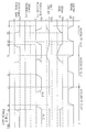
- Fig. 4 illustrates a read-out sequence of the prior art read only memory device, and the cell locations CL11 and CL21 are assumed to be sequentially accessed in the read-out sequence.
- the control signal CB is lifted to the power voltage level Vcc at time t11, and the n-channel enhancement type charging transistor 13 turns on so that the drain node N12 and, accordingly, the common node N11 are coupled with the power voltage line Vcc. Since the n-channel enhancement type transfer transistor Qn21 has turned on, the power voltage line Vcc is further coupled with the digit line DL1 through the n-channel enhancement type transfer transistor Qn21.
- All of the word lines WL1 to WLm are decayed to the low voltage level at time t12.
- the control signal CB remains in the power voltage level.
- the drain node N12 and, accordingly, the common node N11 go up to a predetermined intermediate voltage level V11 lower than the power voltage level Vcc by the threshold level of the charging transistor 13. Since the n-channel enhancement type transfer transistor Qn21 is approximately equal in threshold level to the n-channel enhancement type charging transistor 13, the digit line DL1 is also lifted to the predetermined intermediate voltage level V11, and is balanced with the drain node N12. Thus, the difference between the drain node N12 and the selected digit line DL1 is minimized in this instance.
- the drain node N12 of the predetermined intermediate voltage level V11 causes the n-channel enhancement type field effect transistor Qn42 to turn on, and the common drain node N13 is coupled through the n-channel enhancement type field effect transistor Qn42 with the ground voltage line. For this reason, the output data signal Dout goes down to the low voltage level at time t13.
- the control signal CB is recovered to the low or ground voltage level at time t14, and the n-channel enhancement type charging transistor 13 turns off.
- the row address bits causes the row address decoder unit 16 to lift the word line WL1 upon recovery of the control signal CB, and the n-channel enhancement type memory transistor Qn11 turns on to provide the current path from the associated digit line DL1 to the ground voltage line. Current flows from the digit line DL1 to the ground voltage line, and the digit line DL1 is decayed toward the ground voltage level. The digit line DL1 thus decayed allows the n-channel enhancement type transfer transistor Qn21 to turn on, and, accordingly, the drain node N12 goes down toward the ground voltage level.
- the output inverting circuit 14 couples the power voltage line Vcc through the p-channel enhancement type field effect transistor Qp41 with the common drain node N13, and this results in the output data signal Dout of the high voltage level at time t15.
- the control signal CB goes up at time t16, and the drain node N12 and the digit line DL1 are precharged to the predetermined intermediate voltage level V11 as similar to the access to the cell location CL11.
- the word line WL2 goes up at time t17; however, both of the digit line DL1 and the drain node N12 are kept at the predetermined intermediate voltage level V11, because any current path is not provided from the digit line DL1 to the ground voltage line.
- the drain node N12 at the predetermined intermediate voltage level V11 causes the output inverting circuit 14 to couple the common drain node N13 through the n-channel enhancement type field effect transistor Qn42 with the ground voltage line, and the output data signal Dout remains in the low voltage level.
- the voltage level on the digit line DL1 fluctuates due to the noise.
- the difference between the drain node N12 and the digit line DL1 has been balanced with one another, and the fluctuation on the digit line DL1 is less causative of fluctuation in voltage level at the drain node N12.
- the drain node N12 does not widely swing the voltage level, and, for this reason, the output inverting circuit 14 keeps the output data signal Dout in the low voltage level.
- FIG. 5 of the drawings another read only memory device embodying the present invention is illustrated, and the circuit components thereof are similar to those of the first embodiment except for connections between the drain node N12, the output inverting circuit 14 and the constant voltage generating circuit 15. For this reason, the component elements of the second embodiment are labeled with the same references as the first embodiment.
- the drain node N12 of the n-channel enhancement type charging transistor is coupled with the gate electrode of the p-channel enhancement type load transistor Qp41, and the output node N14 of the constant voltage generating circuit 15 is coupled with the gate electrode of the n-channel enhancement type load transistor Qn42.
- the connections are exchanged, and the connections between the circuit components Qp51 and Qn52 are modified in accordance therewith.
- the block decoder 51 is coupled through decoded signal lines BL1 to BLx with the n-channel enhancement type selecting transistors Qn61 to Qn6x, and selects one of the memory cell sub-arrays 111 to 11x from the memory cell array 11.
- the other circuit components behave on the selected memory cell sub-array as similar to those of the first embodiment, and no further description is incorporated hereinbelow.
- a boosted power voltage level may be supplied to some circuit components for enhancing the stability of circuit behavior.
- the read only memory device may be incorporated in an ultra large scale integration such as, for example, a microprocessor or a semi-custom made integrated circuit device.
- the memory cell arrays 11 of the first to third embodiments are implemented by n-channel enhancement type memory transistors.
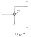
- a memory cell array incorporated in a read only memory device according to the present invention may be implemented by a plurality of floating gate type field effect transistors FG each having the structure shown in Fig. 7.
- the floating gate type field effect transistors FG allows the read only memory device to serve as an electrically programmable read only memory device or as an electrically erasable and programmable read only memory device.
Landscapes
- Read Only Memory (AREA)
Applications Claiming Priority (2)
| Application Number | Priority Date | Filing Date | Title |
|---|---|---|---|
| JP183096/91 | 1991-06-27 | ||
| JP18309691A JP3313383B2 (ja) | 1991-06-27 | 1991-06-27 | 読み出し専用記憶装置 |
Publications (3)
| Publication Number | Publication Date |
|---|---|
| EP0520357A2 true EP0520357A2 (de) | 1992-12-30 |
| EP0520357A3 EP0520357A3 (en) | 1995-04-05 |
| EP0520357B1 EP0520357B1 (de) | 1997-06-04 |
Family
ID=16129697
Family Applications (1)
| Application Number | Title | Priority Date | Filing Date |
|---|---|---|---|
| EP92110515A Expired - Lifetime EP0520357B1 (de) | 1991-06-27 | 1992-06-22 | Festwertspeicher mit Vorladetransistor mit automatischer Stromergänzung am Eingangsknoten des Ausgangsinverters |
Country Status (5)
| Country | Link |
|---|---|
| US (1) | US5274590A (de) |
| EP (1) | EP0520357B1 (de) |
| JP (1) | JP3313383B2 (de) |
| KR (1) | KR950002728B1 (de) |
| DE (1) | DE69220144T2 (de) |
Cited By (1)
| Publication number | Priority date | Publication date | Assignee | Title |
|---|---|---|---|---|
| EP0642132A3 (de) * | 1993-08-02 | 1995-04-05 | Mitsubishi Electric Corp |
Families Citing this family (4)
| Publication number | Priority date | Publication date | Assignee | Title |
|---|---|---|---|---|
| JP2658768B2 (ja) * | 1992-10-19 | 1997-09-30 | 日本電気株式会社 | ダイナミックram |
| JP2894115B2 (ja) * | 1992-11-10 | 1999-05-24 | 松下電器産業株式会社 | カラム選択回路 |
| JPH08293197A (ja) * | 1995-04-21 | 1996-11-05 | Nec Corp | 不揮発性半導体記憶装置 |
| US5706237A (en) * | 1996-10-08 | 1998-01-06 | International Business Machines Corporation | Self-restore circuit with soft error protection for dynamic logic circuits |
Family Cites Families (6)
| Publication number | Priority date | Publication date | Assignee | Title |
|---|---|---|---|---|
| JPS6231094A (ja) * | 1985-08-01 | 1987-02-10 | Toshiba Corp | 不揮発性半導体記憶装置 |
| JPH0766675B2 (ja) * | 1987-07-14 | 1995-07-19 | 株式会社東芝 | プログラマブルrom |
| KR930000963B1 (ko) * | 1988-03-09 | 1993-02-11 | 가부시기가이샤 도오시바 | 불휘발성 메모리 회로장치 |
| JP2507529B2 (ja) * | 1988-03-31 | 1996-06-12 | 株式会社東芝 | 不揮発性半導体記憶装置 |
| JP2513795B2 (ja) * | 1988-07-22 | 1996-07-03 | 沖電気工業株式会社 | Mos型半導体記憶装置 |
| JPH0724298B2 (ja) * | 1988-08-10 | 1995-03-15 | 日本電気株式会社 | 半導体記憶装置 |
-
1991
- 1991-06-27 JP JP18309691A patent/JP3313383B2/ja not_active Expired - Fee Related
-
1992
- 1992-06-22 US US07/901,688 patent/US5274590A/en not_active Expired - Fee Related
- 1992-06-22 EP EP92110515A patent/EP0520357B1/de not_active Expired - Lifetime
- 1992-06-22 DE DE69220144T patent/DE69220144T2/de not_active Expired - Fee Related
- 1992-06-25 KR KR1019920011077A patent/KR950002728B1/ko not_active Expired - Fee Related
Cited By (2)
| Publication number | Priority date | Publication date | Assignee | Title |
|---|---|---|---|---|
| EP0642132A3 (de) * | 1993-08-02 | 1995-04-05 | Mitsubishi Electric Corp | |
| US5438547A (en) * | 1993-08-02 | 1995-08-01 | Mitsubishi Denki Kabushiki Kaisha | Memory-unit sense amplifier |
Also Published As
| Publication number | Publication date |
|---|---|
| KR950002728B1 (ko) | 1995-03-24 |
| JP3313383B2 (ja) | 2002-08-12 |
| EP0520357A3 (en) | 1995-04-05 |
| DE69220144T2 (de) | 1998-01-22 |
| US5274590A (en) | 1993-12-28 |
| DE69220144D1 (de) | 1997-07-10 |
| JPH056686A (ja) | 1993-01-14 |
| EP0520357B1 (de) | 1997-06-04 |
Similar Documents
| Publication | Publication Date | Title |
|---|---|---|
| US4389705A (en) | Semiconductor memory circuit with depletion data transfer transistor | |
| US4094012A (en) | Electrically programmable MOS read-only memory with isolated decoders | |
| KR100681225B1 (ko) | 정확한 내부기준전압을 발생하는 반도체 메모리 장치 | |
| JP2507529B2 (ja) | 不揮発性半導体記憶装置 | |
| US5243573A (en) | Sense amplifier for nonvolatile semiconductor storage devices | |
| US5255233A (en) | Non-volatile semiconductor memory device equipped with sense amplifier circuit for discriminating small differential voltage level | |
| US4709165A (en) | Voltage supply level detecting circuit | |
| EP0199501A2 (de) | CMOS-Stromdetektorverstärker | |
| US6028813A (en) | NOR type semiconductor memory device and a method for reading data stored therein | |
| KR100245244B1 (ko) | 반도체 기억장치 | |
| US6744659B1 (en) | Source-biased memory cell array | |
| US4794571A (en) | Dynamic read-write random access memory | |
| EP0332135B1 (de) | Nichtflüchtige Speicherschaltung mit niedriger Leistung und grossem Betriebsspannungsbereich | |
| US5371703A (en) | Single-bit output type memory including bipolar selection transistors | |
| US6600672B2 (en) | Semiconductor memory device | |
| KR0146862B1 (ko) | 반도체 메모리 장치 | |
| EP0710959A2 (de) | Halbleiteranordnung mit einfachem stabilen Umschaltungsschaltkreis zum selektiven Liefern verschiedener Leistungsspannungen | |
| US5933373A (en) | Semiconductor memory device having constant potential generator for clamping digit lines at constant level allowing precharge transistor to slightly turn on | |
| US6141277A (en) | Semiconductor memory preventing sense amplifier malfunctions due to effects of noise generated in output buffer | |
| US4939691A (en) | Static random access memory | |
| US7099214B2 (en) | Semiconductor memory device | |
| EP0520357B1 (de) | Festwertspeicher mit Vorladetransistor mit automatischer Stromergänzung am Eingangsknoten des Ausgangsinverters | |
| KR910006997A (ko) | 기생용량에 의해 야기된 오동작을 방지하기 위한 eprom의 디코더 회로 | |
| KR910007740B1 (ko) | 비트라인 안정화를 위한 전원전압 추적회로 | |
| US5198998A (en) | Erasable programmable read only memory |
Legal Events
| Date | Code | Title | Description |
|---|---|---|---|
| PUAI | Public reference made under article 153(3) epc to a published international application that has entered the european phase |
Free format text: ORIGINAL CODE: 0009012 |
|
| AK | Designated contracting states |
Kind code of ref document: A2 Designated state(s): DE FR GB |
|
| PUAL | Search report despatched |
Free format text: ORIGINAL CODE: 0009013 |
|
| AK | Designated contracting states |
Kind code of ref document: A3 Designated state(s): DE FR GB |
|
| 17P | Request for examination filed |
Effective date: 19950223 |
|
| GRAG | Despatch of communication of intention to grant |
Free format text: ORIGINAL CODE: EPIDOS AGRA |
|
| 17Q | First examination report despatched |
Effective date: 19960730 |
|
| GRAH | Despatch of communication of intention to grant a patent |
Free format text: ORIGINAL CODE: EPIDOS IGRA |
|
| GRAH | Despatch of communication of intention to grant a patent |
Free format text: ORIGINAL CODE: EPIDOS IGRA |
|
| GRAA | (expected) grant |
Free format text: ORIGINAL CODE: 0009210 |
|
| AK | Designated contracting states |
Kind code of ref document: B1 Designated state(s): DE FR GB |
|
| REF | Corresponds to: |
Ref document number: 69220144 Country of ref document: DE Date of ref document: 19970710 |
|
| ET | Fr: translation filed | ||
| PLBE | No opposition filed within time limit |
Free format text: ORIGINAL CODE: 0009261 |
|
| STAA | Information on the status of an ep patent application or granted ep patent |
Free format text: STATUS: NO OPPOSITION FILED WITHIN TIME LIMIT |
|
| 26N | No opposition filed | ||
| REG | Reference to a national code |
Ref country code: GB Ref legal event code: IF02 |
|
| PGFP | Annual fee paid to national office [announced via postgrant information from national office to epo] |
Ref country code: FR Payment date: 20020610 Year of fee payment: 11 |
|
| PGFP | Annual fee paid to national office [announced via postgrant information from national office to epo] |
Ref country code: GB Payment date: 20020619 Year of fee payment: 11 |
|
| PGFP | Annual fee paid to national office [announced via postgrant information from national office to epo] |
Ref country code: DE Payment date: 20020626 Year of fee payment: 11 |
|
| PG25 | Lapsed in a contracting state [announced via postgrant information from national office to epo] |
Ref country code: GB Free format text: LAPSE BECAUSE OF NON-PAYMENT OF DUE FEES Effective date: 20030622 |
|
| PG25 | Lapsed in a contracting state [announced via postgrant information from national office to epo] |
Ref country code: DE Free format text: LAPSE BECAUSE OF NON-PAYMENT OF DUE FEES Effective date: 20040101 |
|
| GBPC | Gb: european patent ceased through non-payment of renewal fee |
Effective date: 20030622 |
|
| PG25 | Lapsed in a contracting state [announced via postgrant information from national office to epo] |
Ref country code: FR Free format text: LAPSE BECAUSE OF NON-PAYMENT OF DUE FEES Effective date: 20040227 |
|
| REG | Reference to a national code |
Ref country code: FR Ref legal event code: ST |