EP0520450A2 - Halbleiterspeicher - Google Patents
Halbleiterspeicher Download PDFInfo
- Publication number
- EP0520450A2 EP0520450A2 EP92110737A EP92110737A EP0520450A2 EP 0520450 A2 EP0520450 A2 EP 0520450A2 EP 92110737 A EP92110737 A EP 92110737A EP 92110737 A EP92110737 A EP 92110737A EP 0520450 A2 EP0520450 A2 EP 0520450A2
- Authority
- EP
- European Patent Office
- Prior art keywords
- control signal
- bit line
- transfer gate
- potential
- generation circuit
- Prior art date
- Legal status (The legal status is an assumption and is not a legal conclusion. Google has not performed a legal analysis and makes no representation as to the accuracy of the status listed.)
- Granted
Links
Images
Classifications
-
- G—PHYSICS
- G11—INFORMATION STORAGE
- G11C—STATIC STORES
- G11C7/00—Arrangements for writing information into, or reading information out from, a digital store
Definitions
- the present invention relates to a semiconductor memory device, and more particularly, to a semiconductor memory device which is capable of writing a data simultaneously to a plurality of memory cells.
- a dynamic random access memory (DRAM) for video (VRAM) which utilizes the DRAM technology and is suitable as a video memory has been developed and is in widespread use.
- the arrangement location of a data stored in a VRAM corresponds to a display screen.
- a data in a memory cell group on the same word line corresponds to one line portion (one scanning line portion) of the display screen.
- all of the regions for the portion of several lines of the display screen have the same color. In such a case, it takes too long a time if a data is written to each memory cell in order to make these cells to have the same color.
- a technology for writing the same data at once to the memory cell group belonging to the same word line has lately been developed.
- the conventional structure for writing an identical data all at once to the memory cell group belonging to the same word line requires special circuits such as a special purpose circuit for supplying an identical data to every bit line, a special decoder circuit which realizes the simultaneous selection of all of the bit lines or a control circuit which controls the decoder circuit.
- a special purpose circuit for supplying an identical data to every bit line a special decoder circuit which realizes the simultaneous selection of all of the bit lines or a control circuit which controls the decoder circuit.
- the semiconductor memory device comprises a memory cell array which includes a plurality of memory cells arranged in array form in row and column directions, a plurality of bit line pairs that respectively connect these memory cells in common for every column and word lines that respectively connect these memory cells in common for every row, a sense amplifier which is connected to each member of the bit line pair at the one ends of the bit line pair for amplifying the potential difference between the pair of bit lines, a transfer gate provided between one end of the bit line and the sense amplifier, the energization thereof being controlled in response to a transfer gate control signal, a reference potential correction circuit connected to each of the bit line pair between the sense amplifier and the transfer gate for supplying a predetermined potential to one bit line member of the bit line pair in response to a reference potential control signal, a transfer gate control signal generation circuit which generates the transfer gate control signal, and a reference potential control signal generation circuit which generates the reference potential control signal, where in the transfer gate control signal generation circuit is controlled such that during the ordinary operation mode the time at which the transfer gate control signal is
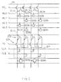
- Word lines WL0 to WL3 and digit lines DL1a, DL1b, DL2a, and DL2b are respectively arranged so as to be orthogonal with each other, and memory cells 503a to 503h are arranged at every other intersection of these lines.
- Each of these memory cells is constituted of one transistor and one capacitor element (not shown).
- the digit lines DL1a to DL2b are used respectively as sets of two lines.
- Information in a memory cell connected to one word line arbitrarily selected appears in lines on one side of the digit lines DL1a to DL2b that are grouped in pairs. Namely, the potential of one of the digit line pair is raised or lowered in response to the information in the memory cell.
- the variation of the potential for a power supply voltage of 5V is 300 to 600 mV.
- This change in the potential affects the information quantity of the memory cells 503a to 503h, and the stray capacitance of the digit lines DL1a to DL2b.
- positive feedback type operational amplifiers (sense amplifiers) 504a and 504b by means of a flip-flop or the like are provided.
- the digit lines DL1a to DL2b are connected to a pre-charge power supply line PG via a plurality of transistors which form the transfer gates whose control terminals are connected respectively to a pre-charge control line PDL.
- a feedback circuit 506 for cutting down the peak current at the time of restoring of information to the memory cells 503a to 503h, and a transfer gate 505 for isolating the stray capacitance of the digit lines DL1a to DL2b which becomes a factor of delay in the amplification speed at the time of amplification of the differential potential.
- a reference potential correction circuit 107 is connected between the respective bit lines and a reference potential control line CLA or CLB in order to correct the unbalance of the operating margin that is generated in the degradation of the information quantity of the memory cell caused by ⁇ rays or the leakage current due to its difference at the times of rise and fall of the digit line potential.
- the reference potential correction circuit 107 is provided between the transfer gate 505 and the sense amplifiers 504a and 504b in this embodiment. Moreover, at the time of simultaneous write mode, the time of closing the transfer gates 505 is earlier than the time of selecting a word line. This operation will be described in more detail later.
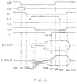
- the ordinary refresh operation will be described. Since, in the standby state, all of the word lines are in the nonselect state and the potential of the pre-charge control line PDL is at a high level (at the time t 200), the digit lines DL1a to DL2b are connected to the pre-charge power supply line PG all to be at the potential same as that of the pre-charge potential. Next, the address ADD of the word line to be refreshed is given, and the refresh operation is started by bringing an external signal RAS ⁇ to a low level (at the time 201).
- the potential of the pre-charge control line PDL is lowered and the digit lines DL1a to DL2b are disconnected from the precharge power supply line PG to be in the floating state (at the time t202).
- the word line (WL1, for example) corresponding to the address information given to the address signal ADD is selected (at the time t203)
- the memory cells 503c and 503d are connected to the digit lines DL1b and DL2b and the potential of the digit line is raised or lowered (see the dotted line in the figure).
- the potentials of the other members of the pairs, DL1a and DL2a do not undergo a change so that there are generated potential difference between the digit lines DL1a and DL1b and between DL2a and DL2b (at the time t204).
- the digit lines DL1a to DL2b and the sense amplifiers 504a and 504b are connected electrically since the transfer gate 505 is open, and the above-mentioned potential differences are transferred as they are to the sense amplifiers.
- the potentials of the digit lines DL1a and DL2a that are not connected to the memory cells 503c and 503d are controlled to be somewhat lower than the potential of the reference potential correction circuit 107 by means of the potential changes in the reference potential control lines CLA and CLB (at the time t205).
- the transfer gate 505 is closed, the amplification operation is carried out at high speed by disconnecting the digit lines DL1a to DL2b from the sense amplifiers 504a and 504b, and the restore operation to the memory cells 503c and 503d by the feedback circuit 506 is started (at the time t206).
- the transfer gate 505 is opened again, and the sense amplifiers 504a and 504b also carry out the restore operation to the memory cells 503c and 503d (at the time t207).
- the external signal RAS ⁇ is returned to the high level (at the time t208)
- the memory cells 503c and 503d are disconnected from the digit lines DL1a to DL2b by returning the word line WL1 to the nonselected state (at the time t209), the digit line is precharged (at the time t210), and returns to the standby state (at the time t211).
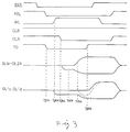
- a reference potential correction circuit 107 is operated in the state where the transfer gate 505 is closed (at the time t303). At this time, the reference potential correction circuit 107 causes the potentials of the reference potential control lines CLA and CLB in response to the data desired to be written to the memory cells. Consequently, potential differences corresponding to the potentials of the reference potential control lines CLA and CLB will be input to the input ends of the sense amplifiers 503c and 503d. In this case, the potential difference is greater in proportion to the portion unaffected by the capacitance of the digit line, and there is generated a potential difference which is sufficient to operate the sense amplifier (at the time t304). As a result of this operation, the identical data is input to all of the sense amplifiers.
- the potential difference given to the sense amplifier at the time t304 is about 140 mV for a power supply voltage of 5V.
- the transfer gate 505 is opened (at the time t306), and the same data are stored simultaneously in the memory cells 503c and 503d. Accordingly, an identical data designated by the reference potential correction circuit 107 is stored in all of the memory cells belonging to one word line that is selected regardless of the data that have been stored there.
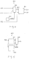
- FIG. 4 An example of construction of reference potential control circuit 300 which supplies a predetermined potential to the reference potential control lines CLA and CLB that control the reference potential operation circuit 107 is shown in FIG. 4.
- the selection operation of the selection circuit 303 is controlled by a made decision circuit 304 which outputs a flag signal MODE under a special input signal condition. Namely, when the flag signal MODE is not output, the ordinary address ADD is input to the reference potential generation circuit 301 the same as in the prior art, whereas when the flag signal MODE is output, a data DIN for simultaneous write which is other than the address is input to the reference potential generation circuit 301.
- the reference potential generation circuit 301 supplies a predetermined potential to the reference potential control lines CLA and CLB in response to the input address 302.
- FIG. 5 An example of constitution of a transfer gate control circuit 400 which generates the transfer gate control signal TG that controls the energization of the transfer gate 505 is shown in FIG. 5.
- a special mode signal generation circuit 402 which generates a transfer control signal waveform to be used at the time of simultaneous write mode, separate from a transfer gate control signal generation circuit 401 which has been used in the past.
- a selection circuit 403 selects the signal from either one of the transfer gate control signal generation circuit 401 or the special mode signal generation circuit 402 in response to the flag signal MODE, and outputs the selected signal as the transfer gate signal TG.
- the transfer gate signal TG output has the waveform of the special mode generation circuit 402, namely, the TG waveform in which the time (t301) at which the transfer gate is closed appears earlier than the time (t302) at which the word line WL1 is selected, as shown in FIG. 3.
- this embodiment makes the simultaneous write operation possible for the prior art semiconductor memory device which was incapable of the simultaneous write operation by a mere change of the arrangement position of the reference potential correction circuit 107 and the addition of simple circuits as shown in FIG. 4 and FIG. 5. Consequently, compared with the conventional semiconductor memory device which required a large scale circuit construction for the simultaneous writing, this embodiment makes the simultaneous writing possible by circuit modifications which scarcely affect the chip size.
Landscapes
- Dram (AREA)
Applications Claiming Priority (2)
| Application Number | Priority Date | Filing Date | Title |
|---|---|---|---|
| JP03183104A JP3084801B2 (ja) | 1991-06-27 | 1991-06-27 | 半導体メモリ装置 |
| JP183104/91 | 1991-06-27 |
Publications (3)
| Publication Number | Publication Date |
|---|---|
| EP0520450A2 true EP0520450A2 (de) | 1992-12-30 |
| EP0520450A3 EP0520450A3 (en) | 1995-03-22 |
| EP0520450B1 EP0520450B1 (de) | 1998-01-07 |
Family
ID=16129848
Family Applications (1)
| Application Number | Title | Priority Date | Filing Date |
|---|---|---|---|
| EP92110737A Expired - Lifetime EP0520450B1 (de) | 1991-06-27 | 1992-06-25 | Halbleiterspeicher |
Country Status (5)
| Country | Link |
|---|---|
| US (1) | US5317539A (de) |
| EP (1) | EP0520450B1 (de) |
| JP (1) | JP3084801B2 (de) |
| KR (1) | KR960013840B1 (de) |
| DE (1) | DE69223857T2 (de) |
Families Citing this family (4)
| Publication number | Priority date | Publication date | Assignee | Title |
|---|---|---|---|---|
| JP3277108B2 (ja) * | 1995-10-31 | 2002-04-22 | インターナショナル・ビジネス・マシーンズ・コーポレーション | Dramアレイ |
| KR100434552B1 (ko) * | 1997-08-21 | 2004-07-16 | 삼성전자주식회사 | 백금/탄소분말과그제조방법,및이를이용하여형성된촉매층을갖는연료전지 |
| JP4000001B2 (ja) * | 2002-04-22 | 2007-10-31 | 松下電器産業株式会社 | クロック制御装置およびクロック制御方法 |
| JP2006164183A (ja) * | 2004-12-10 | 2006-06-22 | Renesas Technology Corp | 半導体信号処理装置 |
Family Cites Families (4)
| Publication number | Priority date | Publication date | Assignee | Title |
|---|---|---|---|---|
| EP0321847B1 (de) * | 1987-12-21 | 1994-06-29 | Kabushiki Kaisha Toshiba | Halbleiterspeicher, der fähig zur Verbesserung der Datenwiedereinschreibgeschwindigkeit ist |
| JPH0770212B2 (ja) * | 1988-07-19 | 1995-07-31 | 日本電気株式会社 | 半導体メモリ回路 |
| JPH0283892A (ja) * | 1988-09-20 | 1990-03-23 | Fujitsu Ltd | 半導体記憶装置 |
| EP0430614B1 (de) * | 1989-12-01 | 1996-02-07 | Matsushita Electronics Corporation | Halbleiterspeicher dynamischen Typs |
-
1991
- 1991-06-27 JP JP03183104A patent/JP3084801B2/ja not_active Expired - Lifetime
-
1992
- 1992-06-25 DE DE69223857T patent/DE69223857T2/de not_active Expired - Fee Related
- 1992-06-25 EP EP92110737A patent/EP0520450B1/de not_active Expired - Lifetime
- 1992-06-26 KR KR1019920011178A patent/KR960013840B1/ko not_active Expired - Fee Related
- 1992-06-29 US US07/905,418 patent/US5317539A/en not_active Expired - Lifetime
Also Published As
| Publication number | Publication date |
|---|---|
| EP0520450B1 (de) | 1998-01-07 |
| US5317539A (en) | 1994-05-31 |
| JPH056655A (ja) | 1993-01-14 |
| KR930001421A (ko) | 1993-01-16 |
| EP0520450A3 (en) | 1995-03-22 |
| DE69223857T2 (de) | 1998-06-18 |
| JP3084801B2 (ja) | 2000-09-04 |
| KR960013840B1 (ko) | 1996-10-10 |
| DE69223857D1 (de) | 1998-02-12 |
Similar Documents
| Publication | Publication Date | Title |
|---|---|---|
| US4367540A (en) | Dynamic memory with an interchangeable pair of data lines and sense amplifiers | |
| US5677865A (en) | Ferroelectric memory using reference charge circuit | |
| KR950000757B1 (ko) | 감지 증폭기를 갖는 반도체 메모리 | |
| JP3551858B2 (ja) | 半導体メモリ装置 | |
| US5815451A (en) | Dynamic semiconductor memory device having a precharge circuit using low power consumption | |
| EP0595747A2 (de) | Spannungsabfühlverfahren durch variabele Bitleitungsvorladung für DRAM Strukturen | |
| US20250292826A1 (en) | Semiconductor storage device | |
| KR100824798B1 (ko) | 에지 서브 어레이에 전체 데이터 패턴을 기입할 수 있는 오픈 비트 라인 구조를 가지는 메모리 코어, 이를 구비한 반도체 메모리 장치, 및 에지 서브 어레이 테스트 방법 | |
| US7012831B2 (en) | Semiconductor memory device | |
| US5761141A (en) | Semiconductor memory device and test method therefor | |
| US5007028A (en) | Multiport memory with improved timing of word line selection | |
| JPH06150646A (ja) | 半導体メモリ | |
| US6707707B2 (en) | SRAM power-up system and method | |
| JP2980368B2 (ja) | ダイナミック型半導体記憶装置 | |
| EP0520450B1 (de) | Halbleiterspeicher | |
| US5719811A (en) | Semiconductor memory device | |
| JP3178946B2 (ja) | 半導体記憶装置及びその駆動方法 | |
| US5619449A (en) | Bit line sensing in a memory array | |
| US5481496A (en) | Semiconductor memory device and method of data transfer therefor | |
| JPH04219689A (ja) | 半導体記憶装置およびその読出方法 | |
| US5504709A (en) | Semiconductor memory device | |
| US6556491B2 (en) | Semiconductor storage device and method of testing the same | |
| US5894440A (en) | Semiconductor memory device and data transferring structure and method therein | |
| US5594681A (en) | Dynamic random access memory wherein timing of completion of data reading is advanced | |
| US5410506A (en) | Memory integrated circuit with protection against disturbances |
Legal Events
| Date | Code | Title | Description |
|---|---|---|---|
| PUAI | Public reference made under article 153(3) epc to a published international application that has entered the european phase |
Free format text: ORIGINAL CODE: 0009012 |
|
| AK | Designated contracting states |
Kind code of ref document: A2 Designated state(s): DE FR GB |
|
| PUAL | Search report despatched |
Free format text: ORIGINAL CODE: 0009013 |
|
| AK | Designated contracting states |
Kind code of ref document: A3 Designated state(s): DE FR GB |
|
| 17P | Request for examination filed |
Effective date: 19950209 |
|
| 17Q | First examination report despatched |
Effective date: 19960426 |
|
| GRAG | Despatch of communication of intention to grant |
Free format text: ORIGINAL CODE: EPIDOS AGRA |
|
| GRAG | Despatch of communication of intention to grant |
Free format text: ORIGINAL CODE: EPIDOS AGRA |
|
| GRAH | Despatch of communication of intention to grant a patent |
Free format text: ORIGINAL CODE: EPIDOS IGRA |
|
| GRAH | Despatch of communication of intention to grant a patent |
Free format text: ORIGINAL CODE: EPIDOS IGRA |
|
| GRAA | (expected) grant |
Free format text: ORIGINAL CODE: 0009210 |
|
| AK | Designated contracting states |
Kind code of ref document: B1 Designated state(s): DE FR GB |
|
| REF | Corresponds to: |
Ref document number: 69223857 Country of ref document: DE Date of ref document: 19980212 |
|
| ET | Fr: translation filed | ||
| PLBE | No opposition filed within time limit |
Free format text: ORIGINAL CODE: 0009261 |
|
| STAA | Information on the status of an ep patent application or granted ep patent |
Free format text: STATUS: NO OPPOSITION FILED WITHIN TIME LIMIT |
|
| 26N | No opposition filed | ||
| REG | Reference to a national code |
Ref country code: GB Ref legal event code: IF02 |
|
| REG | Reference to a national code |
Ref country code: GB Ref legal event code: 732E |
|
| REG | Reference to a national code |
Ref country code: FR Ref legal event code: TQ |
|
| REG | Reference to a national code |
Ref country code: GB Ref legal event code: 732E |
|
| REG | Reference to a national code |
Ref country code: FR Ref legal event code: TQ Ref country code: FR Ref legal event code: TP |
|
| PGFP | Annual fee paid to national office [announced via postgrant information from national office to epo] |
Ref country code: GB Payment date: 20090624 Year of fee payment: 18 Ref country code: DE Payment date: 20090619 Year of fee payment: 18 |
|
| GBPC | Gb: european patent ceased through non-payment of renewal fee |
Effective date: 20100625 |
|
| REG | Reference to a national code |
Ref country code: FR Ref legal event code: ST Effective date: 20110228 |
|
| PG25 | Lapsed in a contracting state [announced via postgrant information from national office to epo] |
Ref country code: DE Free format text: LAPSE BECAUSE OF NON-PAYMENT OF DUE FEES Effective date: 20110101 |
|
| PG25 | Lapsed in a contracting state [announced via postgrant information from national office to epo] |
Ref country code: FR Free format text: LAPSE BECAUSE OF NON-PAYMENT OF DUE FEES Effective date: 20100630 |
|
| PG25 | Lapsed in a contracting state [announced via postgrant information from national office to epo] |
Ref country code: GB Free format text: LAPSE BECAUSE OF NON-PAYMENT OF DUE FEES Effective date: 20100625 |
|
| PGFP | Annual fee paid to national office [announced via postgrant information from national office to epo] |
Ref country code: FR Payment date: 20090611 Year of fee payment: 18 |