EP0595747A2 - Spannungsabfühlverfahren durch variabele Bitleitungsvorladung für DRAM Strukturen - Google Patents
Spannungsabfühlverfahren durch variabele Bitleitungsvorladung für DRAM Strukturen Download PDFInfo
- Publication number
- EP0595747A2 EP0595747A2 EP93480137A EP93480137A EP0595747A2 EP 0595747 A2 EP0595747 A2 EP 0595747A2 EP 93480137 A EP93480137 A EP 93480137A EP 93480137 A EP93480137 A EP 93480137A EP 0595747 A2 EP0595747 A2 EP 0595747A2
- Authority
- EP
- European Patent Office
- Prior art keywords
- bitline
- bitlines
- sensing
- pair
- array
- Prior art date
- Legal status (The legal status is an assumption and is not a legal conclusion. Google has not performed a legal analysis and makes no representation as to the accuracy of the status listed.)
- Withdrawn
Links
Images



Classifications
-
- G—PHYSICS
- G11—INFORMATION STORAGE
- G11C—STATIC STORES
- G11C11/00—Digital stores characterised by the use of particular electric or magnetic storage elements; Storage elements therefor
- G11C11/21—Digital stores characterised by the use of particular electric or magnetic storage elements; Storage elements therefor using electric elements
- G11C11/34—Digital stores characterised by the use of particular electric or magnetic storage elements; Storage elements therefor using electric elements using semiconductor devices
- G11C11/40—Digital stores characterised by the use of particular electric or magnetic storage elements; Storage elements therefor using electric elements using semiconductor devices using transistors
- G11C11/401—Digital stores characterised by the use of particular electric or magnetic storage elements; Storage elements therefor using electric elements using semiconductor devices using transistors forming cells needing refreshing or charge regeneration, i.e. dynamic cells
- G11C11/4063—Auxiliary circuits, e.g. for addressing, decoding, driving, writing, sensing or timing
- G11C11/407—Auxiliary circuits, e.g. for addressing, decoding, driving, writing, sensing or timing for memory cells of the field-effect type
- G11C11/409—Read-write [R-W] circuits
- G11C11/4094—Bit-line management or control circuits
Definitions
- the present invention relates to dynamic random access memory (DRAM) structures and more particularly to a sensing method for DRAM structures using a single-bitline voltage swing and variable bitline precharge voltage.
- DRAM dynamic random access memory
- U.S. Patent 4,669,065 issued May 26, 1987 to Ohsawa and entitled, "DYNAMIC MEMORY APPARATUS HAVING A SENSE AMPLIFIER AND A REFERENCE VOLTAGE CONNECTION CIRCUIT THEREFOR" discloses a memory apparatus that has a dummy cell comprising two sets of series connections of MOS transistors and capacitors, respectively, connected to a pair of bitlines, which are connected to a sense amplifier of a flip-flop type, and a third MOS transistor having a source and a drain thereof connected between junction points of the MOS transistors and the capacitors of the dummy cell.
- the capacitors are charged at a high level potential and a low level potential, respectively, of the bitlines and then they are shorted to each other through the third MOS transistor so that they have a common potential of a middle potential level.
- the potential of the middle level can be supplied to a pair of input terminals to the flip-flop type sense amplifier as a reference potential signal.
- U.S. Patent 4,792,928 issued December 20, 1988 to Tobita entitled, "SEMICONDUCTOR MEMORY CIRCUIT WITH CONTROL OF BITLINE VOLTAGE BALANCING" describes a semiconductor memory circuit that includes a plurality of memory cell columns each comprising a plurality of memory cells connected to a bitline, at least a dummy cell connected to a bitline constituting a bitline pair with said bitline, a sense amplifier connected between said two bitlines, and at least a FET for balancing the voltages of said two bitlines; and a balance control circuit for detecting the termination of selection of a dummy word line which is provided for the control of the dummy cell and thereafter operating the FET.
- U.S. Patent 4,816,706 issued March 28, 1989 to Dhong et al entitled, "SENSE AMPLIFIER WITH IMPROVED BITLINE PRECHARGING FOR DYNAMIC RANDOM ACCESS MEMORY” discloses a sense amplifier and decoupling device structure for integrated circuit memories wherein an embodiment of a cross-coupled sense amplifier includes two PMOS devices, the gates of which devices are grounded and clamp the downward voltage swing of the memory bitlines to the absolute value of the threshold voltage (VTP) of the grounded-gate PMOS devices in the sense amplifier. This limited voltage swing does not affect charge storage of storage capacitors because the absolute value of the threshold voltage (VT) of the cell transfer gate device is larger.
- Precharging the bitlines is achieved by equalizing the two bitlines, each initially charged to VDD and
- One node of the sense amplifier retains a full VDD swing and is conveniently connected to the DATA bus.
- the sense amplifier bitline swing is limited to a swing of VDD -
- U.S. Patent 4,794,571 issued December 27, 1988 to Uchida and entitled, "DYNAMIC READ-WRITE RANDOM ACCESS MEMORY" discloses a DRAM with reduced leakage by biasing the bitlines to a voltage between that of the wordlines and the voltage of the drain of the MOS transistor.
- An object of the present invention is to provide a sensing means for a DRAM which has a low bitline power dissipation.
- Another object of the present invention is to provide a sensing method employing a variable precharge voltage with a single-bitline voltage swing.
- a further object of the present invention is to provide a sensing means for a DRAM wherein the bitline precharge voltage changes from one RAS cycle to the next.
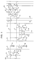
- Fig. 1 is a schematic illustration of a circuit embodiment of a portion of a bitline pair according to the present invention.
- Fig. 2 is a schematic illustration of an embodiment of a memory array according to the present invention.
- Fig. 3 is an illustration of the waveforms of the signals associated with the circuit embodiment of Fig. 1.
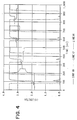
- Fig. 4 and 5 are illustrations of the voltage waveforms present on the bitlines of Fig. 1 during circuit operation.
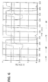
- Fig. 6 is an illustration of the node waveforms of the capacitors of the cells and reference cells of Fig. 1 during circuit operation.
- bitlines are then restored back to V DD /2 during precharge.
- both bitlines dissipate a.c. energy, thus, refresh of a DRAM memory cell of the type wherein both bitlines undergo voltage swings results in energy dissipation on both bitlines.
- Another version of a memory circuit DRAM provides a single-bitline swing sensing scheme where the refresh energy is reduced by holding the reference bitline of a bitline pair at the bitline precharge voltage during sense amplifier latching and subsequent rewrite into one cell. Sensing/rewrite and writing operations of the cell are not affected, since the reference bitline does not need to undergo a voltage swing for the sensing/rewrite and write operations. Thus, the a.c. energy dissipated by the voltage swing on the reference bitline in conventional refresh, read and write operations is eliminated.
- a single-bitline swing DRAM memory circuit is described in co-pending patent application Serial No. 07/729,120 filed July 12, 1991 by S.H. Dhong et al., entitled "POWER SAVING SENSING CIRCUITS FOR DYNAMIC RANDOM ACCESS MEMORY" and which is assigned to the IBM Corporation.
- the present invention provides a new sensing scheme, which uses a floating sensing voltage with single-bitline swing, the bitline power dissipation of which is only 2/3 that of 1/2 V DD sensing for the worst-case pattern.
- the bitline precharge voltage changes from one row address storage (RAS) cycle to the next, depending on the precharge voltage of the previous RAS cycle and the polarity of the data in the accessed cells.
- RAS row address storage
- the new sensing scheme is shown in simplified form in Figure 1.
- Figure 1 the principles of the invention are illustrated in connection with only a single bitline pair.
- the sensing/rewrite scheme involves the voltage on only the bitline connected to the accessed cell undergoing a swing to either the high voltage level stored in the cell, or to the low voltage level stored in the cell to accomplish re-writing of the stored information back into the cell; the complementary bitline in the bitline pair does not undergo such a voltage swing. Assume that a cell will have V DD stored in it for a "1", and a low voltage level at or near ground for a "0".
- bitline precharge voltage depends upon the sequence of data bits sensed previously on the bitline pair; it asymptotically approaches V DD for reading a series of high levels, and asymptotically approaches the cell low level for reading a series of low levels, or will move in between V DD and the low level for sequences that are a mix of "1" and "0" levels.
- V F V S C S C S + C BL + V PRE C BL C S + C BL
- V S V DD 2
- ⁇ V sense is independent of the precharge voltage V PRE .
- the implementation of the new sensing scheme can be explained by following the example waveforms shown in Fig. 4.
- the reference cell capacitance 72 is charged to V DD /2.
- the wordline 14 is activated and reference cell word line 44 is also activated.
- word line 14 causes charge transfer between the cell capacitance C S 88 and the bitline capacitance C BL 89.
- the reference cell word line 44 is accessed, and charge is shared between the bitline capacitance C BL 91 and the reference cell capacitance 72.
- a differential signal between bitlines 10 and 12 is generated, as described above.
- This differential voltage is impressed on the nodes 33 and 35 of the sense amplifier 16 through devices 34 and 36.
- Devices 34 and 36 are then turned off, isolating the nodes of the sense amplifier 16, and the sense amplifier is set in the conventional manner by pulsing node 24 to V DD , and node 26 to ground. Assuming the cell capacitance stored the voltage V DD , the setting of the sense amplifier 16 results in node 35 going to V DD , and node 33 going to ground.
- device 36 is turned back on by a pulse on line 40, causing the bitline 12 to go to V DD , and rewriting V DD back into cell storage capacitance 88.
- the word lines 14 and 44 are deselected, turning off devices 90 and 50, and sense amplifier pulse lines 24 and 26 return to their initial levels, completing the RAS cycle.
- the complementary bitline 10 is not connected to the sense amplifier after the sense amplifier has set, and remains close to the precharge voltage it had at the beginning at the cycle. Detailed waveforms of the signals on various lines are shown in Figure 3.
- bitline 10 and its complement 12 are shorted together and to V eq via line 32 by devices 18, 20, and 22, and equilibrate at a voltage which becomes the bitline precharge voltage for the next RAS cycle.
- This precharge voltage is higher than the precharge voltage of the previous cycle. If the accessed memory cell capacitance 88 had had 0 volts stored on it, the bitline precharge voltage would be lower than that of the previous RAS cycle. If the accessed cell connected to bitline 14 on each subsequent cycle has a high level stored on its cell capacitance, for the following RAS cycles the same sequence is repeated and the bitline precharge voltages increases each cycle.
- bitline power is drawn from the DRAM power supply to equilibrate the bitline pair voltage to the precharge voltage; only redistribution of charge between the bitlines is involved.
- No bitline power is drawn from the supply voltage when the bitline goes from the precharge voltage to the low cell level (i.e. a "0" is sensed). Only when a high level or "1" is sensed does current flow from the power supply into the bitline.
- this power may be greater than for V DD /2 sensing which also uses a single bitline swing, but over a series of cycles, the highest average power dissipation for the new variable precharged voltage sensing scheme occurs when a data pattern of alternating 0's (low levels) and 1's (high levels) (101010107) is read out.
- the precharge voltage will asymptotically approach being at 2/3 V DD and 1/3 V DD on alternate cycles. In this case, the power dissipation is proportional to 1/3 V DD .
- the power dissipation is proportional to 1/2 V DD .
- the new method dissipates 2/3 of the power of that dissipated in the conventional V DD /2 s ensing case in the worst case.
- Conventional V DD /2 sensing dissipates the minimum worst case bitline power of any fixed bitline precharge voltage approach, assuming a stored "1" is V DD and a stored "0" is 0 volts.
- FIG. 2 A preferred embodiment of a memory array according to the present invention is shown in Figure 2, with corresponding waveforms being illustrated in Figs. 3 to 6.
- the array 31 is a conventional two-dimension array of memory cells, with cells connected to word lines running in the x-direction, and cells connected to bitlines running in the Y-direction, and bitlines organized in pairs in a conventional folded bitline arrangement as is well known to those skilled in the art.
- the V eq line 32 is common to all bitline pairs in the array; as a result, the precharge voltage change averages the effect of all the data stored in all the accessed cells in the array, not just that of a single stored bit as is the case described in connection with the embodiment shown in Figure 1.
- a reference cell Since the precharge voltage varies from cycle to cycle, a reference cell must be provided for each bitline in order to sense the bitline signal differentially as shown in Fig. 1.
- the preferred level of the reference cell is the midway between the high and low voltage levels stored in a cell. This requirement is similar to conventional DRAMs, but the method of achieving the mid level in the reference cells is different because of the single-bitline swing and the fact that the bitline precharge voltage may be any level between the high and low levels stored in the cells.
- bitline pairs 10 and 12 shown in Fig. 1 are equalized to the precharge voltage V eq on line 32 by turning on equalizing devices, 18, 20 and 22.
- the signal on lead 25, which controls devices 18, 20 and 22, is high.
- All the bitline pairs in the array precharge to the same voltage through their respective equalizing devices which are connected to line 32.
- Each pair of bitlines must be coupled to an associated V eq through line 32.
- a plurality of bitline pairs may be coupled to the same line 32, requiring a line 32 to be associated with each plurality of bitline pairs.
- all bitline pairs in the array are coupled to the same line 32.
- Leads 24 and 26 are at the same voltage as the precharge voltage, input lead 28 to SA set clock 30 is low as with conventional sensing, and leads 24 and 26 connect to the respective inputs at each sense amplifier for each bitline pair. Maintaining the same precharge voltage on all the bitline pairs in the array of Fig. 2 and also for leads 24 and 26 guarantees that all sense amplifiers 16 for each bitline pair are off at this stage of operation.
- the devices 34 and 36 are on with lines 38 and 40 high. All wordlines and reference wordlines are high, turning off all PMOS cell access transistors.
- the mid level is restored to the reference cells as follows.
- Lead 54 is pulled to V DD by turning on the transistor 56 with the signal on the CHARGEHIGH lead 58 going low.
- the signal on lead 60 goes low and turns on device 62, charging the reference-cell storage capacitor 64 to V DD .
- Lead 60 returns to high and turns off device 62; and lead 54 is pulled low by turning device 66 on and turning device 56 off.
- Turning on device 68 by lowering the signal on lead 70 charges the reference-cell storage capacitor 72 to the low level of the storage capacitor.
- line 54 is floated by turning device 66 off, and capacitors 72 and 64 are equalized to the mid level voltage by turning devices 68 and 62 on.
- signal line 54 is common to the whole array, and its capacitance is much smaller than the total reference-cell storage capacitance, thus the reference-cell capacitors 64 and 72 are equalized to a voltage level substantially midway between the high and low levels stored in a cell capacitor. After equalization, devices 68 and 62 are turned off.
- bitline equalization devices, 18, 20 and 22 are turned off by forcing the signal on line 25 low.
- a wordline, such as 14, is selected and the corresponding reference wordline 44, is also selected and both are pulled low.
- the isolator devices 34 and 36 are turned off by pulling leads 38 and 40 low, isolating the sense amplifier 16, comprising devices 74, 76 and 78 and 80, from the bitline pair.
- the sense amplifier 16 is set by the clock signals on leads 24 and 26 which are generated by the sense amplifier set clock 30 shown in Fig. 2 in a conventional manner. I/O activities are carried out through the bit switch device pair 79 and 81 after the setting of sense amplifier 16. After setting of the sense amplifier 16, only the bitline with the accessed cell, bitline 12 in this case, is moved high or low depending on the data by turning on device 36 with the high level on lead 40. This results in the voltage level stored in the cell capacitance 88 being set in accordance with the voltage on sense amplifier node 35. After setting the voltage level to the cell capacitor 88, the wordline 14 and the reference wordline 44 are pulled high, turning the access transistors of the accessed cell and reference cell off.
- the signals on leads 24 and 26 are then restored to the inactive state after returning the trigger signal on lead 28 to clock 30 to the low level by connecting lines 24 and 26 through devices not shown which short both the lines to V eq .
- the remaining isolator device 34 and the bitline equalization devices 18, 20, and 22 are turned on and generate a new bitline pre-charge voltage.
- Fig. 4 shows the bitline waveforms for three-consecutive reading "1" and Fig. 5 shows the bitline waveforms for three-consecutive reading "0”. Fig. 6 shows the node waveforms of the capacitors of the cell and reference cells during reading "1".
Landscapes
- Engineering & Computer Science (AREA)
- Microelectronics & Electronic Packaging (AREA)
- Computer Hardware Design (AREA)
- Dram (AREA)
Applications Claiming Priority (2)
| Application Number | Priority Date | Filing Date | Title |
|---|---|---|---|
| US969644 | 1978-12-14 | ||
| US07/969,644 US5339274A (en) | 1992-10-30 | 1992-10-30 | Variable bitline precharge voltage sensing technique for DRAM structures |
Publications (2)
| Publication Number | Publication Date |
|---|---|
| EP0595747A2 true EP0595747A2 (de) | 1994-05-04 |
| EP0595747A3 EP0595747A3 (de) | 1995-04-26 |
Family
ID=25515807
Family Applications (1)
| Application Number | Title | Priority Date | Filing Date |
|---|---|---|---|
| EP93480137A Withdrawn EP0595747A3 (de) | 1992-10-30 | 1993-09-21 | Spannungsabfühlverfahren durch variabele Bitleitungsvorladung für DRAM Strukturen. |
Country Status (3)
| Country | Link |
|---|---|
| US (1) | US5339274A (de) |
| EP (1) | EP0595747A3 (de) |
| JP (1) | JP2698030B2 (de) |
Cited By (1)
| Publication number | Priority date | Publication date | Assignee | Title |
|---|---|---|---|---|
| WO1998058380A1 (en) * | 1997-06-19 | 1998-12-23 | Micron Technology, Inc. | Variable voltage isolation gate |
Families Citing this family (25)
| Publication number | Priority date | Publication date | Assignee | Title |
|---|---|---|---|---|
| US5717644A (en) * | 1996-10-09 | 1998-02-10 | International Business Machines Corporation | Apparatus for varying the refresh rate for a DRAM in response to variation in operating voltages and method thereof |
| JP5003396B2 (ja) * | 1996-12-25 | 2012-08-15 | 富士通セミコンダクター株式会社 | 半導体記憶装置 |
| JP4154006B2 (ja) * | 1996-12-25 | 2008-09-24 | 富士通株式会社 | 半導体記憶装置 |
| JP5012388B2 (ja) * | 1996-12-25 | 2012-08-29 | 富士通セミコンダクター株式会社 | 半導体記憶装置 |
| US5825710A (en) * | 1997-02-26 | 1998-10-20 | Powerchip Semiconductor Corp. | Synchronous semiconductor memory device |
| US5850366A (en) * | 1997-07-24 | 1998-12-15 | Texas Instruments Incorporated | Memory array having dummy cells implemented using standard array cells |
| FR2768847B1 (fr) * | 1997-09-23 | 2001-05-18 | St Microelectronics Sa | Dispositif et procede de lecture/re-ecriture d'une cellule-memoire vive dynamique |
| US6292416B1 (en) * | 1998-02-11 | 2001-09-18 | Alliance Semiconductor Corporation | Apparatus and method of reducing the pre-charge time of bit lines in a random access memory |
| US6097649A (en) * | 1998-06-01 | 2000-08-01 | Silicon Magic Corporation | Method and structure for refresh operation with a low voltage of logic high in a memory device |
| US6198681B1 (en) | 2000-02-28 | 2001-03-06 | Micron | Sense amplifier for low voltage memory arrays |
| US6426905B1 (en) * | 2001-02-07 | 2002-07-30 | International Business Machines Corporation | High speed DRAM local bit line sense amplifier |
| US6400629B1 (en) * | 2001-06-29 | 2002-06-04 | International Business Machines Corporation | System and method for early write to memory by holding bitline at fixed potential |
| US6510093B1 (en) * | 2001-10-18 | 2003-01-21 | International Business Machines Corporation | Method and apparatus for cycle time reduction in a memory system using alternating reference cells and isolated sense lines |
| DE10154613B4 (de) * | 2001-11-07 | 2006-11-23 | Infineon Technologies Ag | Verfahren zum Vorladen von Speicherzellen eines dynamischen Halbleiterspeichers beim Power Up sowie Halbleiterspeicher |
| JP2003233989A (ja) * | 2002-02-07 | 2003-08-22 | Fujitsu Ltd | 半導体記憶装置及びプリチャージ方法 |
| US6738300B2 (en) * | 2002-08-26 | 2004-05-18 | International Business Machines Corporation | Direct read of DRAM cell using high transfer ratio |
| US7046564B2 (en) * | 2003-06-30 | 2006-05-16 | Infineon Technologies Ag | Semiconductor memory |
| US7221605B2 (en) * | 2004-08-31 | 2007-05-22 | Micron Technology, Inc. | Switched capacitor DRAM sense amplifier with immunity to mismatch and offsets |
| US7342832B2 (en) * | 2005-11-16 | 2008-03-11 | Actel Corporation | Bit line pre-settlement circuit and method for flash memory sensing scheme |
| US7706176B2 (en) | 2008-01-07 | 2010-04-27 | Qimonda Ag | Integrated circuit, cell arrangement, method for manufacturing an integrated circuit and for reading a memory cell status, memory module |
| US8605528B2 (en) | 2011-11-03 | 2013-12-10 | International Business Machines Corporation | Sense amplifier having an isolated pre-charge architecture, a memory circuit incorporating such a sense amplifier and associated methods |
| WO2013100982A1 (en) * | 2011-12-28 | 2013-07-04 | Intel Corporation | Apparatus and method for improving power delivery in a memory, such as, a random access memory |
| US9875805B2 (en) | 2015-01-23 | 2018-01-23 | Sandisk Technologies Llc | Double lockout in non-volatile memory |
| US9548130B2 (en) | 2015-04-08 | 2017-01-17 | Sandisk Technologies Llc | Non-volatile memory with prior state sensing |
| US9570179B2 (en) | 2015-04-22 | 2017-02-14 | Sandisk Technologies Llc | Non-volatile memory with two phased programming |
Family Cites Families (20)
| Publication number | Priority date | Publication date | Assignee | Title |
|---|---|---|---|---|
| US3806898A (en) * | 1973-06-29 | 1974-04-23 | Ibm | Regeneration of dynamic monolithic memories |
| NL7502375A (nl) * | 1975-02-28 | 1976-08-31 | Philips Nv | Versterkercircuit. |
| JPS60115095A (ja) * | 1983-11-26 | 1985-06-21 | Matsushita Electronics Corp | メモリ装置 |
| JPS60191499A (ja) * | 1984-03-09 | 1985-09-28 | Toshiba Corp | ダイナミツク型ランダムアクセスメモリ |
| JPS60256998A (ja) * | 1984-06-01 | 1985-12-18 | Sharp Corp | ダイナミツク型半導体記憶装置 |
| JPS60258793A (ja) * | 1984-06-04 | 1985-12-20 | Sharp Corp | ダイナミック型半導体記憶装置 |
| US4774691A (en) * | 1985-11-13 | 1988-09-27 | Mitsubishi Denki Kabushiki Kaisha | Semiconductor memory device |
| JPS62197990A (ja) * | 1986-02-25 | 1987-09-01 | Mitsubishi Electric Corp | 半導体記憶回路 |
| JP2508505B2 (ja) * | 1986-07-16 | 1996-06-19 | ソニー株式会社 | 半導体記憶装置 |
| JPH0814988B2 (ja) * | 1987-05-27 | 1996-02-14 | 三菱電機株式会社 | 半導体記憶装置 |
| KR900004635B1 (ko) * | 1987-06-27 | 1990-06-30 | 삼성반도체통신 주식회사 | 반도체 메모리장치의 충전 및 등화회로 |
| US4816706A (en) * | 1987-09-10 | 1989-03-28 | International Business Machines Corporation | Sense amplifier with improved bitline precharging for dynamic random access memory |
| JPH0758592B2 (ja) * | 1987-11-30 | 1995-06-21 | 日本電気株式会社 | 半導体メモリ |
| JPH01171194A (ja) * | 1987-12-25 | 1989-07-06 | Nec Ic Microcomput Syst Ltd | 半導体記憶装置 |
| JPH01171195A (ja) * | 1987-12-25 | 1989-07-06 | Sony Corp | メモリ装置 |
| JPH0229989A (ja) * | 1988-07-19 | 1990-01-31 | Mitsubishi Electric Corp | ダイナミックランダムアクセスメモリ装置 |
| DE58908918D1 (de) * | 1989-03-16 | 1995-03-02 | Siemens Ag | Integrierter Halbleiterspeicher vom Typ DRAM und Verfahren zu seinem Testen. |
| US4998222A (en) * | 1989-12-04 | 1991-03-05 | Nec Electronics Inc. | Dynamic random access memory with internally gated RAS |
| US5036492A (en) * | 1990-02-15 | 1991-07-30 | Advanced Micro Devices, Inc. | CMOS precharge and equalization circuit |
| JPH04271090A (ja) * | 1991-02-27 | 1992-09-28 | Hitachi Ltd | 半導体記憶装置 |
-
1992
- 1992-10-30 US US07/969,644 patent/US5339274A/en not_active Expired - Fee Related
-
1993
- 1993-09-21 EP EP93480137A patent/EP0595747A3/de not_active Withdrawn
- 1993-10-04 JP JP5248067A patent/JP2698030B2/ja not_active Expired - Lifetime
Cited By (4)
| Publication number | Priority date | Publication date | Assignee | Title |
|---|---|---|---|---|
| WO1998058380A1 (en) * | 1997-06-19 | 1998-12-23 | Micron Technology, Inc. | Variable voltage isolation gate |
| US5901078A (en) * | 1997-06-19 | 1999-05-04 | Micron Technology, Inc. | Variable voltage isolation gate and method |
| US6275409B1 (en) | 1997-06-19 | 2001-08-14 | Micron Technology, Inc. | Methods of operating a dynamic random access memory |
| US6445610B1 (en) | 1997-06-19 | 2002-09-03 | Micron Technology, Inc. | Variable voltage isolation gate and method |
Also Published As
| Publication number | Publication date |
|---|---|
| JP2698030B2 (ja) | 1998-01-19 |
| US5339274A (en) | 1994-08-16 |
| JPH06223572A (ja) | 1994-08-12 |
| EP0595747A3 (de) | 1995-04-26 |
Similar Documents
| Publication | Publication Date | Title |
|---|---|---|
| US5339274A (en) | Variable bitline precharge voltage sensing technique for DRAM structures | |
| US5241503A (en) | Dynamic random access memory with improved page-mode performance and method therefor having isolator between memory cells and sense amplifiers | |
| US5677865A (en) | Ferroelectric memory using reference charge circuit | |
| US4855628A (en) | Sense amplifier for high performance dram | |
| US4965767A (en) | Associative memory having simplified memory cell circuitry | |
| US5751626A (en) | Ferroelectric memory using ferroelectric reference cells | |
| US4010453A (en) | Stored charge differential sense amplifier | |
| US4747082A (en) | Semiconductor memory with automatic refresh means | |
| US6266287B1 (en) | Variable equilibrate voltage circuit for paired digit lines | |
| JP4331484B2 (ja) | ランダムアクセスメモリ及びその読み出し、書き込み、及びリフレッシュ方法 | |
| JPH08279290A (ja) | 半導体記憶装置 | |
| EP0830685B1 (de) | Einseitiges lesen unter verwendung von bitleitungen für dram | |
| US5280452A (en) | Power saving semsing circuits for dynamic random access memory | |
| US6301175B1 (en) | Memory device with single-ended sensing and low voltage pre-charge | |
| US5517451A (en) | Semiconductor memory device and memory initializing method | |
| US4439843A (en) | Memory device | |
| US6292417B1 (en) | Memory device with reduced bit line pre-charge voltage | |
| US5625601A (en) | DRAM page copy method | |
| US6097649A (en) | Method and structure for refresh operation with a low voltage of logic high in a memory device | |
| US7012831B2 (en) | Semiconductor memory device | |
| US5894444A (en) | Cell plate referencing for dram sensing | |
| US6535444B2 (en) | Dynamic random access memory device and process for controlling a read access of such a memory | |
| JPH08180688A (ja) | 半導体記憶装置 | |
| EP0920029A2 (de) | RAM-Speicher mit mehreren Zuständen | |
| JPH08249885A (ja) | ダイナミック型半導体記憶装置 |
Legal Events
| Date | Code | Title | Description |
|---|---|---|---|
| PUAI | Public reference made under article 153(3) epc to a published international application that has entered the european phase |
Free format text: ORIGINAL CODE: 0009012 |
|
| AK | Designated contracting states |
Kind code of ref document: A2 Designated state(s): DE FR GB |
|
| 17P | Request for examination filed |
Effective date: 19940819 |
|
| PUAL | Search report despatched |
Free format text: ORIGINAL CODE: 0009013 |
|
| AK | Designated contracting states |
Kind code of ref document: A3 Designated state(s): DE FR GB |
|
| STAA | Information on the status of an ep patent application or granted ep patent |
Free format text: STATUS: THE APPLICATION HAS BEEN WITHDRAWN |
|
| 18W | Application withdrawn |
Withdrawal date: 19960802 |