EP0522712B1 - Thyristor à grille isolée - Google Patents
Thyristor à grille isolée Download PDFInfo
- Publication number
- EP0522712B1 EP0522712B1 EP92305295A EP92305295A EP0522712B1 EP 0522712 B1 EP0522712 B1 EP 0522712B1 EP 92305295 A EP92305295 A EP 92305295A EP 92305295 A EP92305295 A EP 92305295A EP 0522712 B1 EP0522712 B1 EP 0522712B1
- Authority
- EP
- European Patent Office
- Prior art keywords
- layer
- type
- conductive type
- base layer
- drain
- Prior art date
- Legal status (The legal status is an assumption and is not a legal conclusion. Google has not performed a legal analysis and makes no representation as to the accuracy of the status listed.)
- Expired - Lifetime
Links
- 230000015556 catabolic process Effects 0.000 description 77
- 238000009792 diffusion process Methods 0.000 description 47
- 239000000758 substrate Substances 0.000 description 28
- 108091006146 Channels Proteins 0.000 description 25
- 239000012535 impurity Substances 0.000 description 17
- 108010075750 P-Type Calcium Channels Proteins 0.000 description 13
- 238000000034 method Methods 0.000 description 13
- 238000002955 isolation Methods 0.000 description 10
- 238000004519 manufacturing process Methods 0.000 description 8
- 229910021420 polycrystalline silicon Inorganic materials 0.000 description 8
- 229920005591 polysilicon Polymers 0.000 description 8
- XUIMIQQOPSSXEZ-UHFFFAOYSA-N Silicon Chemical compound [Si] XUIMIQQOPSSXEZ-UHFFFAOYSA-N 0.000 description 5
- 229910052710 silicon Inorganic materials 0.000 description 5
- 239000010703 silicon Substances 0.000 description 5
- 108090000699 N-Type Calcium Channels Proteins 0.000 description 3
- 102000004129 N-Type Calcium Channels Human genes 0.000 description 3
- 238000002347 injection Methods 0.000 description 3
- 239000007924 injection Substances 0.000 description 3
- 230000003071 parasitic effect Effects 0.000 description 3
- 230000002093 peripheral effect Effects 0.000 description 3
- 239000004065 semiconductor Substances 0.000 description 3
- 238000013461 design Methods 0.000 description 2
- 239000007943 implant Substances 0.000 description 2
- 238000007796 conventional method Methods 0.000 description 1
- 230000000694 effects Effects 0.000 description 1
- 239000000463 material Substances 0.000 description 1
- 238000012986 modification Methods 0.000 description 1
- 230000004048 modification Effects 0.000 description 1
- 230000003647 oxidation Effects 0.000 description 1
- 238000007254 oxidation reaction Methods 0.000 description 1
- 238000012545 processing Methods 0.000 description 1
- 238000005215 recombination Methods 0.000 description 1
- 230000006798 recombination Effects 0.000 description 1
- 238000010301 surface-oxidation reaction Methods 0.000 description 1
Images









Classifications
-
- H—ELECTRICITY
- H10—SEMICONDUCTOR DEVICES; ELECTRIC SOLID-STATE DEVICES NOT OTHERWISE PROVIDED FOR
- H10D—INORGANIC ELECTRIC SEMICONDUCTOR DEVICES
- H10D18/00—Thyristors
- H10D18/60—Gate-turn-off devices
- H10D18/65—Gate-turn-off devices with turn-off by field effect
- H10D18/655—Gate-turn-off devices with turn-off by field effect produced by insulated gate structures
Definitions
- An n-type drain layer 7 is formed at the position, which is away from the n-type emitter layer 3 at a predetermined distance.
- a gate electrode 10 is formed on the p-type base layer 2 via a gate insulating film 9, and between the n-type drain layer 7 and the n-type cathode layer 3.
- the gate electrode 10 is used for turn-off and comprises an n channel MOSFET in which the n-type emitter layer is used as a source.
- a drain electrode 8 is formed in contact with the p-type base layer 2, and the p-type base layer 2 and the n-type drain layer 7 are short-circuited by the drain electrode 8.
- a positive voltage with respect to the cathode is applied to the insulated gate electrode 10 at the time of turn-off.
- an n-channel is formed under the gate electrode 10.
- a part of hole current which has directly flowed into the n-type emitter layer 3 from the p-type base layer 2 changes its passages and flows into the drain electrode 8 as shown by a broken line, and passes through the n-type drain layer 7 and the portion under the gate electrode 10.
- the hole current is bypassed to the cathode electrode 5 from the n-type emitter layer 3.
- injection of electrons to the p-type base layer 2 from the n-type emitter layer 3 is stopped, and the device is turned off.
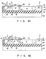
- the p-type channel of the high breakdown voltage device uses a horizontal diffusion region of the diffusion layer
- the p-type channel of the low breakdown voltage device uses a vertical diffusion region of the diffusion layer. Due to this, the layers 33 and 36 are basically different from each other in the amount of implant dose.
- the p-type channel of the high breakdown voltage device uses the horizontal diffusion region of the diffusion layer 33
- the channel length L is determined by the depth of the diffusion. Due to this, it is needed that the diffusion depth in the high breakdown voltage device be independently designed of that in the low breakdown voltage device.
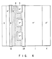
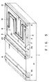
- a gate electrode 24 is formed in a striped pattern on a region of the p-type base layer 2, which is sandwiched by the n-type emitter layer 3 and the n-type base layer 1, via a gate insulating film 23.
- the gate electrode 24 is a turn-on gate electrode, which has been omitted in the embodiment of Fig. 1.
- the cathode electrode 5 and the source electrode 12 are integrally formed such that they are coupled to each other at the peripheral portion as shown in Fig. 2.
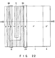
- Figs. 15 to 17 show the layout of the thyristor with an insulated gate of the eighth embodiment of the present invention, and cross sectional views taken along lines XVI-XVI and XVII-XVII of Fig. 15, respectively.
- the relationship between the turn-off MOSFET and the divided n-type emitter layer 3 and the relationship between the drain electrode 8 and the p-type base layer 2 are opposite in terms of the contact position.
- the n-type drain layer 7 is formed in a striped form to be parallel with the divided n-type emitter layer 3.
- the drain electrode 8 contacting the n-type drain layer 7 is formed in a striped form along the the n-type drain layer 7.
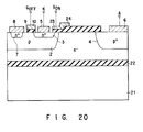
- the convex portions of the n-type drain layer 7 are not covered with the gate electrode 10 (Fig. 20).
- drain electrode 8a is shown not to contact with the p-type base layer 2, it may contact the layer 2.
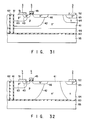
- the seventeenth embodiment of Fig. 32 also shows the horizontal type high breakdown voltage IGBT (or thyristor).
- IGBT or thyristor
- the p-type channel layer 42 and the n-type buffer layer 64 are formed so as to extend to the oxide film 60.
Landscapes
- Thyristors (AREA)
Claims (8)
- Thyristor avec une grille isolée, comprenant:caractérisé en ce que ledit thyristor comprend en outre:une couche de base (1) d'un premier type de conductivité présentant une résistance élevée et comportant une région de surface principale;une couche de base (2) d'un second type de conductivité formée dans une surface de ladite couche de base (1) du premier type de conductivité et comportant une surface adjacente à ladite région de surface principale;une couche d'émetteur (4) du second type de conductivité connectée à ladite couche de base du second type de conductivité via ladite couche de base du premier type de conductivité;une couche d'émetteur (3) du premier type de conductivité formée dans ladite surface de ladite couche de base du second type de conductivité;une première électrode principale (6) formée sur ladite couche d'émetteur (4) du second type de conductivité;une seconde électrode principale (5) formée sur ladite couche d'émetteur (3) du premier type de conductivité,une couche de drain (7) du premier type de conductivité et une couche de source (11) du premier type de conductivité qui sont formées dans ladite surface de ladite couche de base (2) du second type de conductivité;une électrode de drain (8) formée sur ladite couche de drain du premier type de conductivité et comportant une partie qui s'étend jusqu'à une position immédiatement adjacente à ladite couche d'émetteur (3) du premier type de conductivité et qui est agencée en contact avec ladite couche de base (2) du second type de conductivité de manière à mettre en court-circuit ladite couche de base (2) du second type de conductivité avec ladite couche de drain (7) du premier type de conductivité;une électrode de source (12) formée sur ladite couche de source (11) du premier type de conductivité et connectée à ladite seconde électrode principale (5);une électrode de grille isolée de désactivation (10) formée via un film d'isolation de grille (9) sur une région de ladite couche de base (2) du second type de conductivité entre ladite couche de drain (7) du premier type de conductivité et ladite couche de source (11) dudit premier type de conductivité; etune électrode de grille isolée d'activation (24) formée via un film d'isolation de grille (23) sur une région de ladite couche de base (2) du second type de conductivité entre ladite région de surface principale et ladite couche d'émetteur (3) du premier type de conductivité.
- Thyristor selon la revendication 1, caractérisé en outre en ce que ladite surface de ladite couche de base (2) du second type de conductivité affleure ladite région de surface principale.
- Thyristor selon la revendication 2, caractérisé en outre en ce que ladite couche d'émetteur (4) du second type de conductivité est formée dans une surface de ladite couche de base (1) du premier type de conductivité et comporte une surface adjacente à ladite région de surface principale et affleurant celle-ci.
- Thyristor selon l'une quelconque des revendications 1 à 3, caractérisé en outre en ce que ladite couche d'émetteur (3) du premier type de conductivité comprend une pluralité de parties d'émetteur dudit premier type de conductivité définies séparément.
- Thyristor selon la revendication 4, caractérisé en outre en ce que ladite électrode de drain (8) comporte une pluralité de parties dont chacune s'étend entre deux parties adjacentes de ladite pluralité de parties d'émetteur (3) dudit premier type de conductivité.
- Thyristor selon l'une quelconque des revendications 1 à 5, caractérisé en outre en ce que ladite électrode de grille de désactivation est formée selon un motif en zigzag.
- Thyristor selon l'une quelconque des revendications 1 à 6, caractérisé en outre en ce que ladite couche d'émetteur (3) du premier type de conductivité, ladite couche de drain (7) du premier type de conductivité et ladite couche de source (11) du premier type de conductivité sont formées séparément dans ladite surface de ladite couche de base (2) du second type de conductivité et sont placées successivement depuis ladite région de surface principale.
- Thyristor selon l'une quelconque des revendications 1 à 6, caractérisé en outre en ce que ladite couche de source (11) du premier type de conductivité et ladite couche d'émetteur (3) du premier type de conductivité sont unifiées, et ladite électrode de source (12) et ladite seconde électrode principale (5) sont unifiées.
Applications Claiming Priority (4)
| Application Number | Priority Date | Filing Date | Title |
|---|---|---|---|
| JP137894/91 | 1991-06-10 | ||
| JP13789491 | 1991-06-10 | ||
| JP34550191 | 1991-12-26 | ||
| JP345501/91 | 1991-12-26 |
Publications (3)
| Publication Number | Publication Date |
|---|---|
| EP0522712A2 EP0522712A2 (fr) | 1993-01-13 |
| EP0522712A3 EP0522712A3 (en) | 1993-03-10 |
| EP0522712B1 true EP0522712B1 (fr) | 1999-03-24 |
Family
ID=26471061
Family Applications (1)
| Application Number | Title | Priority Date | Filing Date |
|---|---|---|---|
| EP92305295A Expired - Lifetime EP0522712B1 (fr) | 1991-06-10 | 1992-06-10 | Thyristor à grille isolée |
Country Status (3)
| Country | Link |
|---|---|
| US (1) | US5315134A (fr) |
| EP (1) | EP0522712B1 (fr) |
| DE (1) | DE69228721T2 (fr) |
Families Citing this family (3)
| Publication number | Priority date | Publication date | Assignee | Title |
|---|---|---|---|---|
| US5923071A (en) * | 1992-06-12 | 1999-07-13 | Seiko Instruments Inc. | Semiconductor device having a semiconductor film of low oxygen concentration |
| JP3163820B2 (ja) * | 1992-07-28 | 2001-05-08 | 富士電機株式会社 | 半導体装置 |
| US5548150A (en) * | 1993-03-10 | 1996-08-20 | Kabushiki Kaisha Toshiba | Field effect transistor |
Citations (1)
| Publication number | Priority date | Publication date | Assignee | Title |
|---|---|---|---|---|
| JPS609165A (ja) * | 1983-06-29 | 1985-01-18 | Hitachi Ltd | 半導体装置 |
Family Cites Families (12)
| Publication number | Priority date | Publication date | Assignee | Title |
|---|---|---|---|---|
| JPS60196974A (ja) * | 1984-03-19 | 1985-10-05 | Toshiba Corp | 導電変調型mosfet |
| US4672407A (en) * | 1984-05-30 | 1987-06-09 | Kabushiki Kaisha Toshiba | Conductivity modulated MOSFET |
| DE3689680T2 (de) * | 1985-09-30 | 1994-06-23 | Toshiba Kawasaki Kk | Mittels Steuerelektrode abschaltbarer Thyristor mit unabhängigen Zünd-/Lösch-Kontrolltransistoren. |
| US4963951A (en) * | 1985-11-29 | 1990-10-16 | General Electric Company | Lateral insulated gate bipolar transistors with improved latch-up immunity |
| US4860072A (en) * | 1986-03-05 | 1989-08-22 | Ixys Corporation | Monolithic semiconductor device and method of manufacturing same |
| DE3855922T2 (de) * | 1987-02-26 | 1998-01-02 | Toshiba Kawasaki Kk | An-Steuertechnik für Thyristor mit isolierter Steuerelektrode |
| US4912541A (en) * | 1987-05-19 | 1990-03-27 | General Electric Company | Monolithically integrated bidirectional lateral semiconductor device with insulated gate control in both directions and method of fabrication |
| US4857983A (en) * | 1987-05-19 | 1989-08-15 | General Electric Company | Monolithically integrated semiconductor device having bidirectional conducting capability and method of fabrication |
| DE3902300C3 (de) * | 1988-01-30 | 1995-02-09 | Toshiba Kawasaki Kk | Abschaltthyristor |
| EP0329993A3 (fr) * | 1988-02-25 | 1990-03-21 | Siemens Aktiengesellschaft | Thyristor à faible puissance de commande |
| DE58901063D1 (de) * | 1988-03-10 | 1992-05-07 | Asea Brown Boveri | Mos-gesteuerter thyristor (mct). |
| SE463235B (sv) * | 1989-02-23 | 1990-10-22 | Asea Brown Boveri | Mos-faelteffekttransistorstyrd tyristor |
-
1992
- 1992-06-10 EP EP92305295A patent/EP0522712B1/fr not_active Expired - Lifetime
- 1992-06-10 DE DE69228721T patent/DE69228721T2/de not_active Expired - Fee Related
- 1992-06-10 US US07/896,422 patent/US5315134A/en not_active Expired - Lifetime
Patent Citations (1)
| Publication number | Priority date | Publication date | Assignee | Title |
|---|---|---|---|---|
| JPS609165A (ja) * | 1983-06-29 | 1985-01-18 | Hitachi Ltd | 半導体装置 |
Non-Patent Citations (1)
| Title |
|---|
| DATABASE WPI Week 8509, Derwent World Patents Index; Class L03, AN 85-052643 * |
Also Published As
| Publication number | Publication date |
|---|---|
| EP0522712A2 (fr) | 1993-01-13 |
| US5315134A (en) | 1994-05-24 |
| EP0522712A3 (en) | 1993-03-10 |
| DE69228721D1 (de) | 1999-04-29 |
| DE69228721T2 (de) | 1999-10-21 |
Similar Documents
| Publication | Publication Date | Title |
|---|---|---|
| EP1227522B1 (fr) | Dispositif semi-conducteur à tension de claquage élevée | |
| EP0760529B1 (fr) | IGBT latéral | |
| JP3203814B2 (ja) | 半導体装置 | |
| US5714774A (en) | Two-gate semiconductor power switching device | |
| JP3237555B2 (ja) | 半導体装置 | |
| US5559348A (en) | Semiconductor device having insulated gate bipolar transistor | |
| US5343052A (en) | Lateral insulated gate bipolar transistor | |
| US5910664A (en) | Emitter-switched transistor structures | |
| JP7749787B2 (ja) | 半導体装置の駆動方法 | |
| KR20070091259A (ko) | 절연 기판 상에 형성된 전계 효과 트랜지스터 | |
| US5623151A (en) | MOS-gated power semiconductor devices with conductivity modulation by positive feedback mechanism | |
| US5323028A (en) | MOS composite static induction thyristor | |
| US6653666B2 (en) | J-FET semiconductor configuration | |
| US5463231A (en) | Method of operating thyristor with insulated gates | |
| US5608238A (en) | Semiconductor device having two insulated gates and capable of thyristor function and method for operating the same | |
| JPH0851197A (ja) | 電流飽和特性を有するmos制御サイリスタ | |
| US5874767A (en) | Semiconductor device including a lateral power device | |
| JPH09181315A (ja) | 半導体デバイス | |
| US5336907A (en) | MOS gate controlled thyristor having improved turn on/turn off characteristics | |
| EP0522712B1 (fr) | Thyristor à grille isolée | |
| JP2004363477A (ja) | 絶縁ゲート型半導体装置 | |
| JP3249175B2 (ja) | 絶縁ゲート付きサイリスタ及び高耐圧半導体装置 | |
| JPH0575113A (ja) | 絶縁ゲート型サイリスタ | |
| JP3300578B2 (ja) | 絶縁ゲート型電力用半導体装置およびその駆動方法 | |
| JP3278534B2 (ja) | Mosゲート型電力用半導体素子とその駆動方法 |
Legal Events
| Date | Code | Title | Description |
|---|---|---|---|
| PUAI | Public reference made under article 153(3) epc to a published international application that has entered the european phase |
Free format text: ORIGINAL CODE: 0009012 |
|
| 17P | Request for examination filed |
Effective date: 19920708 |
|
| AK | Designated contracting states |
Kind code of ref document: A2 Designated state(s): DE IT |
|
| PUAL | Search report despatched |
Free format text: ORIGINAL CODE: 0009013 |
|
| AK | Designated contracting states |
Kind code of ref document: A3 Designated state(s): DE IT |
|
| 17Q | First examination report despatched |
Effective date: 19940927 |
|
| GRAG | Despatch of communication of intention to grant |
Free format text: ORIGINAL CODE: EPIDOS AGRA |
|
| GRAG | Despatch of communication of intention to grant |
Free format text: ORIGINAL CODE: EPIDOS AGRA |
|
| GRAH | Despatch of communication of intention to grant a patent |
Free format text: ORIGINAL CODE: EPIDOS IGRA |
|
| GRAH | Despatch of communication of intention to grant a patent |
Free format text: ORIGINAL CODE: EPIDOS IGRA |
|
| RBV | Designated contracting states (corrected) |
Designated state(s): DE |
|
| GRAA | (expected) grant |
Free format text: ORIGINAL CODE: 0009210 |
|
| AK | Designated contracting states |
Kind code of ref document: B1 Designated state(s): DE |
|
| REF | Corresponds to: |
Ref document number: 69228721 Country of ref document: DE Date of ref document: 19990429 |
|
| PLBE | No opposition filed within time limit |
Free format text: ORIGINAL CODE: 0009261 |
|
| STAA | Information on the status of an ep patent application or granted ep patent |
Free format text: STATUS: NO OPPOSITION FILED WITHIN TIME LIMIT |
|
| 26N | No opposition filed | ||
| PGFP | Annual fee paid to national office [announced via postgrant information from national office to epo] |
Ref country code: DE Payment date: 20090604 Year of fee payment: 18 |
|
| PG25 | Lapsed in a contracting state [announced via postgrant information from national office to epo] |
Ref country code: DE Free format text: LAPSE BECAUSE OF NON-PAYMENT OF DUE FEES Effective date: 20110101 |