EP0523701A2 - Verfahren zur Herstellung von Elektroden einer Halbleiterschaltung - Google Patents
Verfahren zur Herstellung von Elektroden einer Halbleiterschaltung Download PDFInfo
- Publication number
- EP0523701A2 EP0523701A2 EP92112175A EP92112175A EP0523701A2 EP 0523701 A2 EP0523701 A2 EP 0523701A2 EP 92112175 A EP92112175 A EP 92112175A EP 92112175 A EP92112175 A EP 92112175A EP 0523701 A2 EP0523701 A2 EP 0523701A2
- Authority
- EP
- European Patent Office
- Prior art keywords
- semiconductor device
- film
- contact metal
- metal film
- atoms
- Prior art date
- Legal status (The legal status is an assumption and is not a legal conclusion. Google has not performed a legal analysis and makes no representation as to the accuracy of the status listed.)
- Granted
Links
Images


Classifications
-
- H—ELECTRICITY
- H10—SEMICONDUCTOR DEVICES; ELECTRIC SOLID-STATE DEVICES NOT OTHERWISE PROVIDED FOR
- H10D—INORGANIC ELECTRIC SEMICONDUCTOR DEVICES
- H10D30/00—Field-effect transistors [FET]
- H10D30/60—Insulated-gate field-effect transistors [IGFET]
- H10D30/64—Double-diffused metal-oxide semiconductor [DMOS] FETs
- H10D30/66—Vertical DMOS [VDMOS] FETs
-
- H—ELECTRICITY
- H10—SEMICONDUCTOR DEVICES; ELECTRIC SOLID-STATE DEVICES NOT OTHERWISE PROVIDED FOR
- H10D—INORGANIC ELECTRIC SEMICONDUCTOR DEVICES
- H10D30/00—Field-effect transistors [FET]
- H10D30/01—Manufacture or treatment
- H10D30/021—Manufacture or treatment of FETs having insulated gates [IGFET]
- H10D30/028—Manufacture or treatment of FETs having insulated gates [IGFET] of double-diffused metal oxide semiconductor [DMOS] FETs
- H10D30/0291—Manufacture or treatment of FETs having insulated gates [IGFET] of double-diffused metal oxide semiconductor [DMOS] FETs of vertical DMOS [VDMOS] FETs
-
- H—ELECTRICITY
- H10—SEMICONDUCTOR DEVICES; ELECTRIC SOLID-STATE DEVICES NOT OTHERWISE PROVIDED FOR
- H10D—INORGANIC ELECTRIC SEMICONDUCTOR DEVICES
- H10D62/00—Semiconductor bodies, or regions thereof, of devices having potential barriers
- H10D62/80—Semiconductor bodies, or regions thereof, of devices having potential barriers characterised by the materials
- H10D62/83—Semiconductor bodies, or regions thereof, of devices having potential barriers characterised by the materials being Group IV materials, e.g. B-doped Si or undoped Ge
-
- H—ELECTRICITY
- H10—SEMICONDUCTOR DEVICES; ELECTRIC SOLID-STATE DEVICES NOT OTHERWISE PROVIDED FOR
- H10D—INORGANIC ELECTRIC SEMICONDUCTOR DEVICES
- H10D64/00—Electrodes of devices having potential barriers
- H10D64/01—Manufacture or treatment
- H10D64/011—Manufacture or treatment of electrodes ohmically coupled to a semiconductor
- H10D64/0111—Manufacture or treatment of electrodes ohmically coupled to a semiconductor to Group IV semiconductors
- H10D64/0112—Manufacture or treatment of electrodes ohmically coupled to a semiconductor to Group IV semiconductors using conductive layers comprising silicides
-
- H—ELECTRICITY
- H10—SEMICONDUCTOR DEVICES; ELECTRIC SOLID-STATE DEVICES NOT OTHERWISE PROVIDED FOR
- H10D—INORGANIC ELECTRIC SEMICONDUCTOR DEVICES
- H10D64/00—Electrodes of devices having potential barriers
- H10D64/60—Electrodes characterised by their materials
- H10D64/62—Electrodes ohmically coupled to a semiconductor
-
- Y—GENERAL TAGGING OF NEW TECHNOLOGICAL DEVELOPMENTS; GENERAL TAGGING OF CROSS-SECTIONAL TECHNOLOGIES SPANNING OVER SEVERAL SECTIONS OF THE IPC; TECHNICAL SUBJECTS COVERED BY FORMER USPC CROSS-REFERENCE ART COLLECTIONS [XRACs] AND DIGESTS
- Y10—TECHNICAL SUBJECTS COVERED BY FORMER USPC
- Y10S—TECHNICAL SUBJECTS COVERED BY FORMER USPC CROSS-REFERENCE ART COLLECTIONS [XRACs] AND DIGESTS
- Y10S438/00—Semiconductor device manufacturing: process
- Y10S438/906—Cleaning of wafer as interim step
Definitions
- the present invention relates to a method of forming electrodes of a semiconductor device, and particularly to a method in which adhesive property to a Si substrate is high and is suitable when it is used for forming a back electrode of power devices.
- the former method has a disadvantage such that the increased number of steps incurs higher cost and the polishing incurs crack failure.
- the latter method can make the stress of a nickel film to less than 3 x 10⁸ N/m2 by controlling argon pressure to more than 12 mTorr and the substrate to a temperature of 100°C - 250 °C, thus achieving a certain degree of effect.
- the temperature inside the system increases to 250 °C more.
- the nickel film stress becomes higher, thus causing peel-off at the bonded portion as well.
- the present invention was made to overcome the above problems. It is an object of the present invention to provide a method of forming electrodes of a semiconductor device which can increase the adhesion between a Si substrate and a metal electrode without especially increasing the number of steps such as the formation of a surface with a roughness of specific shape on a Si substrate and without specially decreasing the stress of the nickel film.
- the electrode forming method according to the present invention is characterized in that; in an electrode forming method for a semiconductor device which includes the steps of forming a contact metal film on a silicon substrate surface after subjecting it to a cleaning process using a reverse sputtering process by argon ion, and forming a nickel film as a soldering metal on the contact metal film, the number of the argon atoms per unit area at the interface between the silicon and the contact metal film is controlled to a predetermined value, that is, below 4.0 x 10¹⁴ atoms/cm2.
- the number of argon atoms per unit area at the interface is adjusted to below a predetermined value by controlling the output of the reverse sputtering during the cleaning process.
- the substrate temperature during the formation of the contact metal film when by controlling the substrate temperature during the formation of the contact metal film to about more than 300 ⁇ C, utilizing the diffusion, and the argon atom distribution at the interface between the silicon substrate and the contact metal film is dispersed, whereby the number of argon atoms per unit area at the interface is controlled to less than the predetermined value.
- the present inventors found the fact as a result of many experiments and considerations that in the substrate cleaning process being performed as a preliminary treatment to form a contact metal film on the surface of a silicon substrate, when the oxide film on a silicon substrate in dry process is intended to remove, the adhesion between the silicon substrate and the metal electrode is decreased remarkably.
- the substrate cleaning process it was found that argon atoms introduced into the silicon substrate are a factor which decreases the adhesion strength at the interface between the silicon substrate and the contact metal film in comparison with the strong film stress of a nickel film.
- the present invention was made based on the fact that vigorous studies by the present inventors found that the adhesion strength can make strong by controlling the amount of argon atoms at the interface.
- the natural oxide film grown on the surface of a silicon substrate is removed to clean the surface thereof by bombarding inert argon gas against the silicon substrate.
- the ion bombardment damages the surface of a silicon substrate and the silicon (Si) on the top surface of it makes into amorphous.
- Si when a metal for ormic contact such as titanium (Ti) is deposited, Si diffuses into Ti layer in the Si/Ti interface to form a Si-Ti amorphous layer, whereby the bonding of the Si/Ti interface is strengthened.
- a metal for ormic contact such as titanium (Ti)
- Ti titanium
- Si diffuses into Ti layer in the Si/Ti interface to form a Si-Ti amorphous layer, whereby the bonding of the Si/Ti interface is strengthened.
- argon atoms (Ar) existing in the surface of the Si substrate cannot be easily diffused into Ti layer, but concentrate in the interface between the Si substrate and the Si-Ti amorphous layer.
- the amount of argon atoms which concentrate in the interface can be adjusted by controlling the output of argon ion reverse sputtering during the substrate cleaning process to control the energy of the argon ions.
- the present invention was made based on the result that the present inventors found through many experiments and considerations that the adhesion strength between an electrode and Si can be increased by controlling the substrate temperature during sputtering when an electrode is formed by sputtering.
- argon atoms (Ar) existing on the surface of a Si substrate can be diffused into Ti layer during Ti depositing process at a substrate temperature of more than 300 °C. Therefore Ti can be readily reacted with amorphous Si in the Si/Ti interface without concentrating argon in the interface between the Si substrate and the electrode layer, whereby a strong bonding between electrode and Si can be maintained.
- argon atoms in the interface between the silicon substrate and the contact metal film are controlled in amount, which is introduced into a silicon substrate during the substrate cleaning process and affects adversely to the adhesion strength between the electrode and Si.
- the condition of the argon ion reverse sputtering in the substrate cleaning process, or the substrate temperature to at least 300 ⁇ C during the contact metal formation is controlled merely there is the excellent effect that the amorphous layer of Si and the contact metal is functioned as a strong bonding layer of the interface between electrode and Si substrate, whereby the adhesion strength between the si substrate and the metal electrode can be improved effectively.
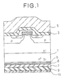
- Fig. 1 is a vertical cross sectional view showing a semiconductor device (DMOS element) manufactured by applying an embodiment according to the present invention.
- Fig. 2 is a structural diagram of a sputtering system used for the embodiment according to the present invention.
- Figs. 3 (a) to 3(f) are cross-sectional views showing diagrammatically a laminated metal electrode manufactured by the first embodiment according to the present invention in order of the manufacturing steps.
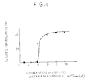
- Fig. 4 is a characteristic diagram showing the relationship between the number of Ar atoms per unit area and Ti-Si peel-off area ratio.
- Fig. 5 is a model diagram showing the peeling mechanism of a Ti-Si interface.
- Figs. 6(a) and 6(f) are cross-sectional views showing a laminated metal electrode manufactured according to the second embodiment of the present invention in order of the manufacturing steps.
- Fig. 7 is a diagram showing the thickness of an amorphous Si layer existing in the surface of a silicon substrate before and after an Ar reverse sputtering process.
- Fig. 8 is a characteristic diagram showing the relationships between substrate temperature and Ti-Si peel-off area ratio.
- Fig. 9 is a diagram explaining the junction mechanism of a Si-Ti interface.
- Fig. 1 is a vertical cross-sectional view showing a semiconductor device (DMOS element) manufactured by applying the first embodiment according to the present invention.
- DMOS element semiconductor device
- the present embodiment will be explained below in conjunction with the manufacturing steps shown in Fig 3.
- Figs. 3(a) to 3(f) show diagrammatically and sequentially the step flows for manufacturing a laminated metal electrode according to the present embodiment.
- the predetermined gate and source regions (not shown) for a power MOS transistor are formed in a 5-inch diameter, 600 ⁇ m thick silicon (Si) substrate.
- an aluminum line 3 acting as a surface electrode is formed in a predetermined pattern.
- a nitride silicon (SiN) layer 5 acting as a passivation film is formed using plasma CVD process to protect the aluminum line 3.
- the silicon substrate 1 is transferred to the sputtering system as shown in Fig. 2 to form a metal film working as the drain electrode of a MOS transistor on the back surface of the silicon substrate 1.
- the sputtering system shown in Fig. 2 is the XM-8 model, DC parallel plate magnetron sputtering system made by Varian Co.
- the sputtering is performed under the conditions that the substrate temperature is about 20 ⁇ C and the pressure of argon (Ar) gas 21 introduced in the chamber 23 is 7.5 mTorr.
- the argon gas is introduced into the chamber 23 from the gas inlet 53 through the massflow meter 51.
- the vacuum pump system comprises a rotary pump 55, a turbo pump 57, and a cryopump 59.
- the rotary pump 55 conducts a rough evacuation
- the turbo pump 57 conducts an intermediate evacuation and an evacuation of the lock chamber 61
- the cryopump 59 conducts a final evacuation.
- the transferring lock table 27 receive a wafer from the transport 25, and in turn descends to transfer it to a shuttle (not shown).
- the shuttle is constructed so as to move along the broken line shown in Fig. 2, and first moves the received wafer onto the process table 29.
- a RF power source is connected so as to apply the lower potential to the process table 29 and the higher potential (or ground potential) to the capture 31.
- the sputtering is performed at a low output of 15 W for a short period of 90 seconds.
- the ionized Ar gas bombards the back surface of the silicon substrate 1, and etches the top surface of the back side by about 2.5 nm.
- the etching removes the natural oxide film of about 2 nm grown on the top surface as well as a contaminant such as carbon.
- the argon gas bombardment also converts the top surface of the silicon substrate into an amorphous.
- the amount of argon atoms existing in the amorphous Si layer was 2.0 x 10¹⁴ atoms/cm2.
- the capture 31 is used to collect contaminants (natural oxide film and the like) on the silicon surface.
- numeral 33 represents a magnet for enclosing electrical discharge.
- a wafer is transferred in the station (Ti film forming chamber) 15 using the shuttle, and then placed on the process table 35.
- a DC power source is connected so as to apply the higher potential (or ground potential) to the process table 35 and the lower potential to the target 37 containing titanium (Ti).
- a sputtering is performed under the condition of the output of 2 kW for 75 seconds.
- the ionized argon gas bombards the target 37 and Ti atoms sputtered out of the target 37 are deposited on the silicon substrate 1 to form a Ti film 7 of a thickness of about 250 nm.
- an Si-Ti amorphous layer 8 is formed in the interface between the silicon substrate 1 and the Ti film 7, as shown in Fig. 3(d).
- numeral 6 represents an amorphous Si layer containing Ar atoms.
- the wafer is transferred into the station (Ni film forming chamber) 17 using the shuttle and then arranged it on the process table 39.
- a DC power source in the station 17 is connected so as to apply the higher potential to the process table 39 and the lower potential to the target 41 containing nickel (Ni).
- Ar gas ionized by sputtering at an output of 1 kW for 249 seconds bombards the target 41.
- the Ni atoms sputtered out of the target 41 are deposited on the Ti film 7 to form a Ni film 9 having a thickness of about 600 nm, as shown in Fig. 3(e).
- the wafer is transferred to the station (Au film forming chamber) 19 using the shuttle and then arranged on the process table 43.
- a DC power source is connected so as to apply the higher potential to the process table 43 and the lower potential to the target 45 containing gold (Au).
- Au atoms are deposited on the Ni film 9 by sputtering at the output of 0.5 kW for 12 seconds to form an Au film 11 of about 50 nm thick, as shown in Fig. 3(f).
- the wafer on which Ti, Ni, Au are deposited sequentially to form a back electrode on the back surface is sent to the transfer lock table using the shuttle, and is send to the transport 49 through the lifting operation of the transfer lock table. Thereafter, the semiconductor device is manufactured as shown in Fig. 1.
- the detailed structure of the power MOS transistor has been omitted.
- the structure may be applied for bipolar elements, diodes and the like, in addition to the well-known MOS structures.
- Fig. 4 shows the relationships between the number of argon atoms per unit area, existing in a Si substrate during an argon etching which is performed prior to the Ti film deposition in the step shown in Fig. 3(d), and the results of peeling-off test which is done to the back electrode of Ti, Ni, Au formed actually.
- the peeling-off test is a method of pasting an adhesive tape on the back of a 5 mm square chip (adhesion strength of about 80 N/m) and then examining the state of the chin from which the adhesion tape is peeled off.
- Fig. 4 shows the results in the case of the substrate temperature of 20 °C. The same result as that seen in Fig. 4 was obtained even by forming the electrode at the substrate temperature of about 350 °C. It was been confirmed the fact that the peeling between Si and ti does not occur when the number of argon atoms per unit area is less than about 4.0 x 10¹⁴ atoms/cm2.
- the silicon atoms in the substrate surface diffuse easily into a Ti film during the Ti film deposition, but the argon atoms diffused into the substrate during the reverse sputtering process do not diffuse and concentrate in the interface between a Si-Ti diffusion layer and a Si substrate, so that the argon atoms concentrated in the interface which does not contribute the bonding between Si and Ti deteriorates the adhesion strength, thus causing peeling.
- the number of argon atoms per unit area, existing in the silicon substrate is less than about 4.0 x 10¹⁴ atoms/cm2
- a strong adhesion strength can be obtained because of the small amount of argon atoms.
- the number of Ar atoms exceeds the above mentioned value, it is considered that the peeling-off occurs due to the Ar concentration at the interface.
- the substrate temperature is over about 350 °C, argon can be diffused.
- the number of Ar atoms existing in the interface covers the above mentioned range.
- This mechanism can be supported by performing micro-analysis of peeled surfaces.
- Table 1 shows the results obtained by analyzing the peeled surfaces of Si/Ti layer which is formed at a substrate temperature of 20 °C and has the argon atom amount of 6.0 x 10¹⁴ atoms/cm2 remaining in the silicon substrate, using X-ray Photoelectron Spectroscopy.
- the number of argon atoms per unit area introduced into the silicon substrate is adjusted to less than 4.0 x 10¹⁴ atoms/cm2, that is, 2.0 x 10¹⁴ atoms/cm2 by controlling the sputtering condition.
- Ar atoms which does not contribute to the bonding of the Si/Ti interface concentrates during the deposition of the Ti film 7 a strong bonding can be maintained by the Si-Ti amorphous layer 8 without affecting the Si-Ti bonding, whereby the bonding between Si and Ti can be made strong sufficiently with respect to the film stress of the Ni film 9.
- the substrate it is not necessary not only to make the substrate with special rough back surface, but also to increase the number of the steps. Furthermore, since the natural oxide film on the back surface of a substrate is removed using Ar reverse sputtering without etching with HF-based etchant, it is possible to remove contamination due to organic material such as carbon without requiring an increased number of steps and a large sized manufacturing apparatus.
- the adhesion strength obtained at the Si-Ti amorphous layer does not require any annealing step for improving adhesion strength after the formation of a Ti/Ni/Au film. As a result, it is possible to prevent an increased number of steps because of additional thermal processing, Au spiking of Ni, and solder wetting failure caused by diffusion and oxidation to the top surface.
- the thermal processing causes a degraded adhesion strength due to the alloy layer with many voids formed between Ti film and Ni film as well as a large warp of wafer.
- a strong bonding can be achieved even at a lower substrate temperature of, for example, 20 °C during a formation of an electrode on the back surface, the aluminum electrode line formed on the surface of a silicon substrate is not deteriorated thermally.
- Figs. 6(a) to 6(f) show diagrammatically a laminated metal electrode formed according to the present embodiment in the order of the manufacturing steps. Like numerals are provided to the same elements as those seen in the first embodiment.
- a silicon (Si) substrate 1 of, for example, 5 inch in diameter and 600 ⁇ m in thickness
- an aluminum line 3 acting as a surface electrode is formed in a predetermined pattern, as shown in Fig. 6(b).
- a nitride silicon (SiN) acting as a passivation film is formed using plasma CVD process to protect the aluminum line 3.
- the silicon substrate is transferred to the sputtering system as shown in Fig. 2 to form a metal film for the drain electrode of the MOS transistor on the back surface of the silicon substrate 1.
- the pressure of the argon (Ar) gas 21 supplied into the chamber 23 is 5 mTorr.
- the sputtering condition differs from that of the first embodiment.
- the sputtering is carried out under the condition that an output for stable electric discharge is 70W and a sputtering time is 180 seconds.
- the ionized argon (Ar+) gas bombards the back surface of the silicon substrate 1 and etches the back surface by about 180 ⁇ .
- the etching removes the natural oxide film grown on the back surface and contamination by carbon or other element. In this time, as shown in Fig. 7, amorphous Si layer due to a damage from the etching exists in the back surface of the substrate.
- the substrate 1 is heated at a substrate temperature of 300°C to 500 °C, for example, 400 °C, in the station (Ti film forming chamber) 15 which is equipped with a heater (not shown).
- a Ti film 7 of about 250nm thick is formed on the silicon substrate 1 by sputtering under the condition of at 2kW for 75 seconds which is the same as that in the first embodiment.
- the Ar atoms implanted into the silicon substrate are diffused by the substrate heating process using the heater and, the above mentioned damage layer or the amorphous Si layer disappears.
- the Si-Ti amorphous layer 8 is formed at the interface between the silicon substrate 1 and the Ti film 7.
- a sputtering is performed at 1 kW for 240 seconds in the station (Ni film forming chamber) 17 to form a Ni film 9 with a thickness of about 600 nm as shown in Fig. 6(e).
- a sputtering is carried out at 0.5 kW for 12 seconds in the station (Au film forming chamber) 19 to form an Au film 11 with a thickness of about 50 nm on the Ni film 9, whereby a semiconductor device shown in Fig. 1 is made as shown in Fig. 6(f).
- Fig. 8 shows the relationship between the substrate temperature determined by means of a heater for Ti film deposition during the step shown in Fig. 6(d), and the results of the peeling-off test to the back electrode of Ti, Ni, and Au formed actually.
- the reverse sputtering is carried out under the condition for the step shown in Fig. 6(d).
- Fig. 8 also shows the result of the peeling-off test where the substrate back etching using Ar reverse sputtering was not performed prior to the Ti film deposition .
- the top surface of the silicon substrate 1 is SiO2, as shown in Fig. 9(a), it does not react with the Ti film 7, whereby a film peeling occurs.
- the natural oxide film SiO2 grown on the top surface of the silicon substrate 1 is removed but the top surface thereof is damaged.
- the top surface is converted into an amorphous Si.
- the Si/Ti interface does not make in nature a titanium siliside with a strong bond at a temperature of less than 550 °C.
- the reverse sputtering is determined on condition that the amount of Ar atoms at the electrode/Si interface is less than 4.0 x 10¹⁴ atoms/cm2. But in the case where a special measure for the argon revere sputtering is not taken, as shown in the present embodiment, it is considered that argon atoms which concentrates at the interface between Si and Si/Ti amorphous layer diffuses easily into the Ti film when the substrate temperature is more than 300 °C.
- Fig. 9(c) it is considered that the strong adhesiveness does not cause a film peeling.
- the substrate temperature is less than 300 °C, the presence of the amorphous Si layer or Ar atoms in the amorphous Si layer decreases the strength, a film peeling occurs, as shown in Fig 9(b).
- the back surface electrode is formed at a substrate of 300°C to 500 °C after the top surface of a substrate is cleaned using Ar reverse sputtering prior to a deposition of the Ti film 7.
- a Ti deposition process to the silicon substrate since Ti reacts easily with the amorphous Si layer existing in the top surface of a Si substrate, an amorphous layer of Si-Ti is formed, while the Ar atoms existing in amorphous Si layer are distributed through diffusion.
- the number of Ar atoms which remain in the interface between the Si substrate and the contact metal film is less than 4.0 x 10¹⁴ atoms/cm2 and the junction between.
- Si layer and Ti layer can be made strong sufficiently with respect to the film stress of the Ni film 9, in no relation with the absolute amount of Ar introduced into the Si substrate.
- the substrate temperature during Ti deposition is less than 500 °C, the heat deterioration of an aluminum electrode formed on the surface of a silicon substrate does not occur.
- the Ti layer 7 is formed as an example to make an ohmic contact with the surface of a wafer.
- Ti for example, chrome (Cr), vanadium (V), zirconium (Zr), aluminum (Al), or gold (Au) may be formed for an ohmic contact.
- the thickness of Ti film can be 100nm to 400 nm, without being limited to 250 nm.
- the thickness of the Ni layer can be 200nm to 1000 nm, without being limited to 600 nm.
- the first and second embodiments show that not only Ti film 7 but also Ni film 9 and Au film 11 are formed at the same substrate temperature as that for a deposition of the Ti film 7.
- the effect of the present invention is improved further if the film stress of a Ni film is made less than 3 x 10⁸ N/m2 by controlling accurately the substrate temperature to 100°C to 250 °C and the Ar pressure during a Ni film formation to more than 12 mTorr.
- the number of Ar atoms existing in the Si substrate may be less than 4.0 x 10¹⁴ atoms/cm2 as shown in the first embodiment and the substrate temperature may be determined more than about 300 °C only during Ti film formation as shown in the second embodiment.
- a Ni film may be formed on the structure obtained above.
Landscapes
- Electrodes Of Semiconductors (AREA)
Applications Claiming Priority (4)
| Application Number | Priority Date | Filing Date | Title |
|---|---|---|---|
| JP03176870A JP3127494B2 (ja) | 1991-07-17 | 1991-07-17 | 半導体装置の電極形成方法 |
| JP176870/91 | 1991-07-17 | ||
| JP3295897A JP2979792B2 (ja) | 1991-11-12 | 1991-11-12 | 半導体装置の電極形成方法 |
| JP295897/91 | 1991-11-12 |
Publications (3)
| Publication Number | Publication Date |
|---|---|
| EP0523701A2 true EP0523701A2 (de) | 1993-01-20 |
| EP0523701A3 EP0523701A3 (en) | 1993-09-29 |
| EP0523701B1 EP0523701B1 (de) | 1998-01-07 |
Family
ID=26497625
Family Applications (1)
| Application Number | Title | Priority Date | Filing Date |
|---|---|---|---|
| EP92112175A Expired - Lifetime EP0523701B1 (de) | 1991-07-17 | 1992-07-16 | Verfahren zur Herstellung von Elektroden eines Halbleiterbauelements |
Country Status (3)
| Country | Link |
|---|---|
| US (1) | US5360765A (de) |
| EP (1) | EP0523701B1 (de) |
| DE (1) | DE69223868T2 (de) |
Cited By (4)
| Publication number | Priority date | Publication date | Assignee | Title |
|---|---|---|---|---|
| EP0812009A3 (de) * | 1996-06-03 | 1998-01-07 | Texas Instruments Incorporated | Verbesserungen in der oder in Bezug auf die Halbleiterherstellung |
| EP1128423A3 (de) * | 2000-02-25 | 2004-03-10 | Murata Manufacturing Co., Ltd. | Flip-Chip montierte elektronische Vorrichtung mit Mehrlagen-Elektroden |
| WO2007049087A1 (en) * | 2005-10-24 | 2007-05-03 | Infineon Technologies Ag | Semiconductor chip with amorphous crack-stop layer |
| CN110034016A (zh) * | 2019-03-25 | 2019-07-19 | 华中科技大学 | 一种半导体芯片正面铝层可焊化方法 |
Families Citing this family (12)
| Publication number | Priority date | Publication date | Assignee | Title |
|---|---|---|---|---|
| US5783487A (en) * | 1996-02-20 | 1998-07-21 | Motorola, Inc. | Method of coupling titanium to a semiconductor substrate and semiconductor device thereof |
| US20040222083A1 (en) * | 1999-09-06 | 2004-11-11 | Su-Chen Fan | Pre-treatment for salicide process |
| TW423052B (en) * | 1999-09-06 | 2001-02-21 | Taiwan Semiconductor Mfg | Preprocess of metal silidation manufacturing process |
| JP2001148367A (ja) * | 1999-11-22 | 2001-05-29 | Nec Corp | 半導体装置の製造方法及び半導体装置の製造装置 |
| US6358821B1 (en) | 2000-07-19 | 2002-03-19 | Chartered Semiconductor Manufacturing Inc. | Method of copper transport prevention by a sputtered gettering layer on backside of wafer |
| US6689687B1 (en) * | 2001-02-02 | 2004-02-10 | Advanced Micro Devices, Inc. | Two-step process for nickel deposition |
| JP2007194514A (ja) | 2006-01-23 | 2007-08-02 | Mitsubishi Electric Corp | 半導体装置の製造方法 |
| US7595257B2 (en) * | 2006-08-22 | 2009-09-29 | Freescale Semiconductor, Inc. | Process of forming an electronic device including a barrier layer |
| JP5283326B2 (ja) * | 2006-10-27 | 2013-09-04 | 三菱電機株式会社 | 半導体装置およびその製造方法 |
| JPWO2010109572A1 (ja) | 2009-03-23 | 2012-09-20 | トヨタ自動車株式会社 | 半導体装置 |
| IT1402530B1 (it) * | 2010-10-25 | 2013-09-13 | St Microelectronics Srl | Circuiti integrati con retro-metallizzazione e relativo metodo di produzione. |
| JP2015204301A (ja) | 2014-04-10 | 2015-11-16 | 三菱電機株式会社 | 半導体装置および半導体装置の製造方法 |
Family Cites Families (15)
| Publication number | Priority date | Publication date | Assignee | Title |
|---|---|---|---|---|
| US3461054A (en) * | 1966-03-24 | 1969-08-12 | Bell Telephone Labor Inc | Cathodic sputtering from a cathodically biased target electrode having an rf potential superimposed on the cathodic bias |
| US3516915A (en) * | 1968-05-01 | 1970-06-23 | Bell Telephone Labor Inc | Sputtering technique |
| US3945903A (en) * | 1974-08-28 | 1976-03-23 | Shatterproof Glass Corporation | Sputter-coating of glass sheets or other substrates |
| US3982908A (en) * | 1975-11-20 | 1976-09-28 | Rca Corporation | Nickel-gold-cobalt contact for silicon devices |
| JPS56142633A (en) * | 1980-04-08 | 1981-11-07 | Mitsubishi Electric Corp | Forming method for back electrode of semiconductor wafer |
| US4513905A (en) * | 1983-07-29 | 1985-04-30 | The Perkin-Elmer Corporation | Integrated circuit metallization technique |
| US4588343A (en) * | 1984-05-18 | 1986-05-13 | Varian Associates, Inc. | Workpiece lifting and holding apparatus |
| JPS6119778A (ja) * | 1984-07-05 | 1986-01-28 | Canon Inc | アモルフアス半導体薄膜の製造方法 |
| JPH084095B2 (ja) * | 1985-03-26 | 1996-01-17 | 日本電気株式会社 | 半導体装置の製造方法 |
| EP0266205B1 (de) * | 1986-10-31 | 1993-12-15 | Nippondenso Co., Ltd. | Bipolarer Halbleitertransistor |
| JPS63290268A (ja) * | 1987-05-20 | 1988-11-28 | Fujitsu Ltd | 薄膜の成長方法 |
| JPH0640066B2 (ja) * | 1987-07-27 | 1994-05-25 | 日本電気株式会社 | 密着力測定装置 |
| JPH0648729B2 (ja) * | 1988-02-24 | 1994-06-22 | シーメンス、アクチエンゲゼルシシヤフト | 電界効果制御可能のバイポーラ・トランジスタ |
| JPH0784647B2 (ja) * | 1988-09-15 | 1995-09-13 | 日本電装株式会社 | ニッケル膜およびそれを形成するスパッタリング方法 |
| JPH02230756A (ja) * | 1989-03-03 | 1990-09-13 | Seiko Epson Corp | 銅電極配線材料 |
-
1992
- 1992-07-16 DE DE69223868T patent/DE69223868T2/de not_active Expired - Fee Related
- 1992-07-16 EP EP92112175A patent/EP0523701B1/de not_active Expired - Lifetime
- 1992-07-17 US US07/914,623 patent/US5360765A/en not_active Expired - Lifetime
Cited By (5)
| Publication number | Priority date | Publication date | Assignee | Title |
|---|---|---|---|---|
| EP0812009A3 (de) * | 1996-06-03 | 1998-01-07 | Texas Instruments Incorporated | Verbesserungen in der oder in Bezug auf die Halbleiterherstellung |
| US6004871A (en) * | 1996-06-03 | 1999-12-21 | Texas Instruments Incorporated | Implant enhancement of titanium silicidation |
| EP1128423A3 (de) * | 2000-02-25 | 2004-03-10 | Murata Manufacturing Co., Ltd. | Flip-Chip montierte elektronische Vorrichtung mit Mehrlagen-Elektroden |
| WO2007049087A1 (en) * | 2005-10-24 | 2007-05-03 | Infineon Technologies Ag | Semiconductor chip with amorphous crack-stop layer |
| CN110034016A (zh) * | 2019-03-25 | 2019-07-19 | 华中科技大学 | 一种半导体芯片正面铝层可焊化方法 |
Also Published As
| Publication number | Publication date |
|---|---|
| DE69223868T2 (de) | 1998-09-03 |
| EP0523701B1 (de) | 1998-01-07 |
| EP0523701A3 (en) | 1993-09-29 |
| US5360765A (en) | 1994-11-01 |
| DE69223868D1 (de) | 1998-02-12 |
Similar Documents
| Publication | Publication Date | Title |
|---|---|---|
| EP0523701A2 (de) | Verfahren zur Herstellung von Elektroden einer Halbleiterschaltung | |
| JP4497737B2 (ja) | 半導体装置の製造方法 | |
| KR100364919B1 (ko) | 결함이개선된CoSi2형성에의한디프(deep)서브-미크론MOSFET의실리사이드화접합부형성방법및MOSFET반도체소자 | |
| US20080083611A1 (en) | High-adhesive backside metallization | |
| US5605724A (en) | Method of forming a metal conductor and diffusion layer | |
| JP3787366B2 (ja) | 背面を金属化した半導体及びその製造方法 | |
| US6117771A (en) | Method for depositing cobalt | |
| US4702941A (en) | Gold metallization process | |
| EP0363673B1 (de) | Durch Zerstäubung abgeschiedene Nickelschicht und Verfahren zu deren Abscheidung | |
| JPH07161659A (ja) | 半導体装置およびその製造方法 | |
| US5739046A (en) | Method of making a reliable barrier layer | |
| EP0477990B1 (de) | Verfahren zum Verbessern der Eigenschaften einer Dünnschicht auf einem Substrat | |
| US5451544A (en) | Method of manufacturing a back contact for semiconductor die | |
| KR100616765B1 (ko) | 확산 접합된 스퍼터 타켓 조립체 및 그 제조 방법 | |
| JP3127494B2 (ja) | 半導体装置の電極形成方法 | |
| EP0463362B1 (de) | Halbleiteranordnung mit Metallschichten | |
| JPS6257255A (ja) | 化合物半導体装置の製造方法 | |
| JP2979792B2 (ja) | 半導体装置の電極形成方法 | |
| EP4375394A1 (de) | Verfahren zum betrieb einer pvd-vorrichtung | |
| US6119921A (en) | Bonding of aluminum oxide components to silicon substrates | |
| JP2979702B2 (ja) | 半導体装置の電極形成方法 | |
| JP2906855B2 (ja) | 半導体装置の製造方法 | |
| EP0260232B1 (de) | Verfahren zur Herstellung ohmischen Metallhalbleiterkontakten | |
| JP3700322B2 (ja) | 半導体装置及びその製造方法 | |
| Tin et al. | Effects of RF bias on remote microwave plasma assisted etching of silicon in SF 6 |
Legal Events
| Date | Code | Title | Description |
|---|---|---|---|
| PUAI | Public reference made under article 153(3) epc to a published international application that has entered the european phase |
Free format text: ORIGINAL CODE: 0009012 |
|
| AK | Designated contracting states |
Kind code of ref document: A2 Designated state(s): DE FR GB |
|
| PUAL | Search report despatched |
Free format text: ORIGINAL CODE: 0009013 |
|
| AK | Designated contracting states |
Kind code of ref document: A3 Designated state(s): DE FR GB |
|
| 17P | Request for examination filed |
Effective date: 19931104 |
|
| 17Q | First examination report despatched |
Effective date: 19951107 |
|
| GRAG | Despatch of communication of intention to grant |
Free format text: ORIGINAL CODE: EPIDOS AGRA |
|
| GRAG | Despatch of communication of intention to grant |
Free format text: ORIGINAL CODE: EPIDOS AGRA |
|
| GRAH | Despatch of communication of intention to grant a patent |
Free format text: ORIGINAL CODE: EPIDOS IGRA |
|
| RAP1 | Party data changed (applicant data changed or rights of an application transferred) |
Owner name: DENSO CORPORATION |
|
| GRAH | Despatch of communication of intention to grant a patent |
Free format text: ORIGINAL CODE: EPIDOS IGRA |
|
| GRAA | (expected) grant |
Free format text: ORIGINAL CODE: 0009210 |
|
| AK | Designated contracting states |
Kind code of ref document: B1 Designated state(s): DE FR GB |
|
| REF | Corresponds to: |
Ref document number: 69223868 Country of ref document: DE Date of ref document: 19980212 |
|
| ET | Fr: translation filed | ||
| REG | Reference to a national code |
Ref country code: GB Ref legal event code: 746 Effective date: 19980916 |
|
| PLBE | No opposition filed within time limit |
Free format text: ORIGINAL CODE: 0009261 |
|
| STAA | Information on the status of an ep patent application or granted ep patent |
Free format text: STATUS: NO OPPOSITION FILED WITHIN TIME LIMIT |
|
| 26N | No opposition filed | ||
| REG | Reference to a national code |
Ref country code: GB Ref legal event code: IF02 |
|
| PGFP | Annual fee paid to national office [announced via postgrant information from national office to epo] |
Ref country code: DE Payment date: 20080724 Year of fee payment: 17 |
|
| PGFP | Annual fee paid to national office [announced via postgrant information from national office to epo] |
Ref country code: FR Payment date: 20080718 Year of fee payment: 17 |
|
| PGFP | Annual fee paid to national office [announced via postgrant information from national office to epo] |
Ref country code: GB Payment date: 20080716 Year of fee payment: 17 |
|
| GBPC | Gb: european patent ceased through non-payment of renewal fee |
Effective date: 20090716 |
|
| REG | Reference to a national code |
Ref country code: FR Ref legal event code: ST Effective date: 20100331 |
|
| PG25 | Lapsed in a contracting state [announced via postgrant information from national office to epo] |
Ref country code: FR Free format text: LAPSE BECAUSE OF NON-PAYMENT OF DUE FEES Effective date: 20090731 |
|
| PG25 | Lapsed in a contracting state [announced via postgrant information from national office to epo] |
Ref country code: GB Free format text: LAPSE BECAUSE OF NON-PAYMENT OF DUE FEES Effective date: 20090716 |
|
| PG25 | Lapsed in a contracting state [announced via postgrant information from national office to epo] |
Ref country code: DE Free format text: LAPSE BECAUSE OF NON-PAYMENT OF DUE FEES Effective date: 20100202 |