EP0523893A2 - Circuit terminal d'un générateur de polarisation de ligne pour réseau ECL - Google Patents
Circuit terminal d'un générateur de polarisation de ligne pour réseau ECL Download PDFInfo
- Publication number
- EP0523893A2 EP0523893A2 EP92306188A EP92306188A EP0523893A2 EP 0523893 A2 EP0523893 A2 EP 0523893A2 EP 92306188 A EP92306188 A EP 92306188A EP 92306188 A EP92306188 A EP 92306188A EP 0523893 A2 EP0523893 A2 EP 0523893A2
- Authority
- EP
- European Patent Office
- Prior art keywords
- transistor
- current
- power supply
- supply source
- emitter
- Prior art date
- Legal status (The legal status is an assumption and is not a legal conclusion. Google has not performed a legal analysis and makes no representation as to the accuracy of the status listed.)
- Granted
Links
Images

Classifications
-
- G—PHYSICS
- G05—CONTROLLING; REGULATING
- G05F—SYSTEMS FOR REGULATING ELECTRIC OR MAGNETIC VARIABLES
- G05F3/00—Non-retroactive systems for regulating electric variables by using an uncontrolled element, or an uncontrolled combination of elements, such element or such combination having self-regulating properties
- G05F3/02—Regulating voltage or current
- G05F3/08—Regulating voltage or current wherein the variable is DC
- G05F3/10—Regulating voltage or current wherein the variable is DC using uncontrolled devices with non-linear characteristics
- G05F3/16—Regulating voltage or current wherein the variable is DC using uncontrolled devices with non-linear characteristics being semiconductor devices
- G05F3/20—Regulating voltage or current wherein the variable is DC using uncontrolled devices with non-linear characteristics being semiconductor devices using diode- transistor combinations
- G05F3/26—Current mirrors
- G05F3/265—Current mirrors using bipolar transistors only
-
- H—ELECTRICITY
- H03—ELECTRONIC CIRCUITRY
- H03K—PULSE TECHNIQUE
- H03K19/00—Logic circuits, i.e. having at least two inputs acting on one output; Inverting circuits
- H03K19/02—Logic circuits, i.e. having at least two inputs acting on one output; Inverting circuits using specified components
- H03K19/08—Logic circuits, i.e. having at least two inputs acting on one output; Inverting circuits using specified components using semiconductor devices
- H03K19/082—Logic circuits, i.e. having at least two inputs acting on one output; Inverting circuits using specified components using semiconductor devices using bipolar transistors
- H03K19/086—Emitter coupled logic
Definitions
- the present invention relates to a termination circuit in an ECL array of a row bias generator.
- This embodiment to be described relates generally to emitter-coupled logic (ECL) gate arrays and more particularly, it relates to a low voltage current mirror termination circuit for an ECL gate array having output emitter followers so as to reduce power consumption without compromising its operating speed.
- ECL emitter-coupled logic
- an ECLmacro-cell function is typically formed of a multi-level transistor structure and an output emitter follower, which performs specified logical functions and is based on an identified circuit principle.
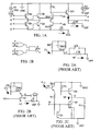
- Figure 1Aa a conventional two-level ECL macroceii function which performs OR/AND logical operations.
- Figure 1 B The symbolic representation of the OR/AND logical operations of Figure 1A is illustrated in Figure 1 B.
- the first level includes a pair of input transistors Qa, Qb and a first reference transistor Qra.
- An input signal A is applied to the base of the transistor Qa
- an input signal B is applied to the base of the transistor Qb
- a first reference voltage VA is applied to the base of the transistor Qra.
- the second level includes a pair of input transistors Qc, Qd and a second reference transistor Qrb.
- An input signal C is connected to the base of the transistor Qc
- an input signal D is connected to the base of the transistor Qd
- a second reference voltage VB is connected to the base of the transistor Qrb.
- a first power supply source GND which is typically at 0 volts, is connected to the collectors of the input transistors Qa, Qb.
- a switch current Is is coupled between the common emitters of the transistors Qc, Qd and Qrb and a second power supply source VEE, which is typically at -5.0 volts.
- an output emitter follower transistor Qo whose emitter provides a first output X.
- a diode is connected between the first output X and a second output Y.
- An emitter follower reference current source lef is connected between the second output Y and a separate emitter follower power supply source VEF.
- the amount of the emitter follower reference current lef being drawn through the output emitter follower transistor Qo is typically equal to two or three times the value of the switch current Is. Accordingly, the amount of power consumption by an array of ECL macrocell functions similar to Figure 1A may be significantly reduced by decreasing the voltage of the emitter follower power supply source VEF.
- a low voltage current mirror termination circuit used with an ECL gate array for providing a constant output emitter follower reference current which is independent of voltage variations in a separate emitter follower power supply source.
- the termination circuit includes a lateral PNP transistor, an NPN mirror transistor, at least one pull-down transistor, and at least one NPN output emitter follower transistor.
- the lateral transistor has its emitter connected to a first power supply source and its base coupled to receive a base bias voltage, and its collector connected to a mirror bias line.
- the mirror transistor has its base and collector connected to the mirror bias line and its emitter connected to the separate power supply source.
- the pull-down transistor has its base connected to the mirror bias line, its collector connected to an output terminal, and its emitter connected to the separate power supply source.
- the output emitter follower transistor has its base coupled to receive an ECL output logic signal, its collector connected to the first power supply source, and its emitter connected to the collector of the pull-down transistor.
- the current through the collector of the pull-down transistor defines the constant output emitter follower reference current which is proportional to the current through the collector of the lateral transistor defining a mirror current.
- FIG. 2A of the drawings there is shown a prior art emitter follower termination circuit 2 referred to as a resistive termination which includes an output emitter follower transistor Qo whose emitter (output X) is connected to a lower voltage of the emitter follower power supply source VEF through an emitter resistor R.
- the power supply source VEF may be made as small as a logic swing V L (voltage change between the level signifying a logic "1" and the level signifying a logic "0") allows and the value of the resistor R is chosen to provide the appropriate fall time.
- This voltage swing at the output X is provided by the change in the voltage across the resistor RL.
- the tolerances of the resistor R and the power supply source VEF will cause variations in the reference current lef and thus the fall time will be changed.
- the emitter follower power supply source VEF tends to be quite noisy.
- Figure 2B depicts a second prior art emitter follower termination circuit 4 referred to as a current source termination which includes an output emitter follower transistor Qo whose emitter (output X) is connected to a lower voltage of the emitter follower power supply source VEF through a current source transistor Qf and an emitter resistor R.
- the base of the transistor Qf is biased by a supply reference voltage VS.
- the reference current lefthen flows through the emitter resistor R.
- Practical low impedance distribution networks for the reference voltage VS requires a voltage drop of 2 V be (V be of transistor Qo and V be of transistor Qf) plus an IR drop relative to the first or top rail power supply source GND. Further, the reference voltage VS itself must be regulated relative to a bottom rail.
- the reference voltage VS is limited by the allowable number of logic levels. However, if the bottom rail is a separate emitter follower power supply source VEF then a distribution network will be required which is essentially a duplication of the reference voltage VS that powers the ECL gate. As a result, a significant power penalty is encountered when used in a large ECL gate array. With this limitation, the practical value of the minimum voltage of the emitter follower power supply source is approximately -3.3 volts (3 V be + I x RL + VEF tolerance).
- FIG. 2C there is illustrated a third prior art emitter follower termination circuit 6 referred to as a current mirror termination which includes a current source transistor Qn, an emitter resistor R, and a current mirror formed of transistors Qx and Qf.
- the base of the transistor Qn is connected to a regulated bias voltage VX.
- the emitter of the transistor Qn is connected to the mirror bias line M via the emitter resistor R.
- the emitter (output X) of the emitter follower transistor Qo is connected to the lower voltage of the source VEF through the mirror transistor Qf.
- the reference current lefflowing through the mirror transistor Qf is determined by the area ratio of emitters of the transistors Qf, Qx; the bias voltage VX; and the value of the resistor R.
- the regulated bias voltage VX limits the minimum voltage of the emitter follower power supply source VEF to approximately -3.0 volts. Further, a duplicate distribution network is also required since the current mirror termination is not referenced to a second power supply source VEE.
- the mirror bias line M is limited to local distribution because of the debiasing of the base-emitter drops of the transistors Qf and Qx.
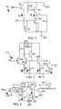
- FIG 4 there is shown a schematic diagram of a typical reference voltage buffer 8 which may be used to generate the required reference voltage VS and the bias voltage VX for the circuits of Figures 2B and 2C, respectively.
- the reference voltage buffer 8 is comprised of transistors Q1-Q5, resistors Rr and Re, and current sources 11-13.
- the base of the transistor Q1 receives a regulated reference voltage VZ, which is from a bandgap reference generator (not shown).
- the reference voltage VS is a V be plus an IR drop relative to the power supply source VEF
- the bias voltage VX is 2 V be plus an IR drop relative to the source VEF.
- the minimum voltage of the power supply source VEF is 3 V be + lr x Rr + Is x Re s 3.5 volts.
- a power consumption due to the output emitter follower transistors can be as much as 2 to 3 watts on large ECL gate arrays (i.e., more than 20,000 gates). Assuming that the average power dissipated per array gate is on the order of 1 or 2 mW, there could be conserved one watt of power by lowering the voltage of the emitter follower power supply reference VEF by one volt. This is enough power for operating another 1,000 array gate. Therefore, it would be desirable to provide a low voltage current mirror termination circuit 10 ( Figure 3) of the present invention for an ECL gate array having output emitter followers so as to reduce power consumed by a separate emitter follower power supply source VEF.
- the present low voltage current mirror termination circuit be adaptable for use with a typical reference voltage buffer of Figure 4 for supplying the voltages VS and VX and suffers no speed penalty when ECL gate array users make changes in the voltage of the emitter follower power supply source VEF so as to accommodate their needs.
- FIG. 3 a schematic circuit diagram of a low voltage current mirror termination circuit 10 of the present invention.
- the termination circuit 10 provides an emitter follower reference current lef which has constant current characteristics whose current level is substantially unaffected by variations in the voltage of the emitter follower power supply source VEF that is connected to the termination circuit.
- the termination circuit includes a lateral PNP mirror transistor Qp and current mirror formed of transistors Qx and Qf.
- the base of the transistor Qp is connected to a base bias voltage VEP.
- the mirror transistor Qp has its emitter connected to the first power supply source GND, and its collector connected directly to a mirror bias line M.
- the NPN current mirror transistor Qx is connected in a diode fashion with its base and collector connected to the mirror line M and its emitter connected to the lower voltage of the emitter follower power supply source VEF.
- the NPN pull-down transistor Qf has an emitter area A times larger than the NPN transistor Qx.
- the pull-down transistor Qf has its base connected to the mirror line M, its collector connected to the emitter (output X) of the output emitter follower transistor Qo, and its emitters connected to the source VEF.
- the emitter follower reference current lef flowing through the transistor Qf is determined by the relative emitter areas of the transistors Qf and Qx, and the mirror current Ip flowing through the collector of the lateral PNP transistor Qp.
- the base bias voltage VEP is a V be drop below the first power supply source GND or top rail and the mirror bias line M is a V be drop above the separate emitter follower power supply source VEF.
- the minimum voltage of the source VEF is thus no longer restricted by the distribution network for the bias voltage VX or the reference voltage VS, or by the local component biases such as the base-to-emitter voltage of the transistor QX and the saturation voltage V ee(sat) of the transistor Qp, but is determined by the voltage swing V L at the output X plus the saturation voltage of the transistor Qf. Therefore, the minimum voltage for the source VEF could be as low as -2.0 volts relative to the top rail. As a result, power consumption required by the output emitter follower transistor Qo would be approximately sixty percent less than the -5.0 volts for the source VEF and operating at the same speed.
- FIG 5 there is shown a simplified circuit representation of a macrocell row in a large gate array, illustrating how the termination circuit 10 in Figure 3 of the present invention may be used.
- a typical large ECL gate array is constructed of a plurality of matrix blocks (i.e., 4, 6 or more) each block containing a plurality of macrocell rows.
- each of the macrocell rows would have a plurality of macrocell functions.
- Each of the macrocell functions may be of a structure similar to that of Figure 1.
- each matrix block in the array may be formed of 16 macrocell rows with each macrocell row having 16 macrocell functions so as to provide a total of 256 macrocell functions.
- Figure 5 shows only a single macrocell row in one of the plurality of matrix blocks and the associated components connected therewith which are directed to the present invention.
- Each of the macrocell functions include a low voltage current mirror termination circuit 10 similar to Figure 3 which consists of a lateral PNP transistor Qp, an NPN mirror transistor Qx, and at least one pull-down transistor Qf having one or more emitters so as to permit metal programming (i.e., desired speed/power levels). It will be noted that only the transistors Qx and Qf of the macrocell function M1 are shown. While the lateral transistor Qp and the output emitter follower transistor Qo ( Figure 3) are actually a part of the present termination circuit 10, the lateral transistor Qp in each of the macrocell functions M1-M16 have been separated therefrom so as to define the single macrocell row 14.
- a row bias generator 16 is used to provide the base bias voltage VEP for the bases of the lateral transistors Qp1-Qp16 and consists of a current source transistor QN, a lateral PNP transistor QPL, and a vertical PNP transistor QPV.
- the base of the transistor QN is connected to reference voltage VS which is obtained from the buffer of Figure 4.
- the base bias voltage VEP at node 18 is connected to the bases of the lateral transistors Qp1-Qp16 of the termination circuit 10 through metal traces of the base rail on line 26 which are represented by resistances Rb.
- the emitter of the lateral transistor QPL of the row bias generator 16 is connected at node 20 to the first power supply source GND at node 22 via metal traces of the top rail 24 which are represented by resistances Rt.
- Each of the metal traces are of an uniform length L in each macrocell function.
- collector current Ic of the current source transistor QN is the sum of the collector current of the lateral transistor QPL and the base current of the vertical transistor QPV, which is: where B v is the beta of the transistor QPV.
- the emitter current lr which is set by the resistor R, of the current source transistor QN becomes: where an is the alpha of the transistor QN.
- the mirror current Ip in equation (3) is approximately ⁇ n l r .
- the mirror current Ip and thus the emitter follower reference current lef has been shown to be virtually independent of the process parameters of the PNP transistor Qp and is determined by setting the reference voltage VS. Accordingly, the output emitter follower reference current lef will track the current source Is and the alpha of the NPN transistors in the macrocell function.
- the single emitter resistor R in the row bias generator 16 is used to set the current Ir and thus the current lef rather than by resistors in macrocell functions M1-M16, the single resistor R can be made of a higher tolerance with minimal area penalty and with the attendant power saving.
- the lateral PNP transistors i.e., Qp1-Qp16
- the lateral PNP transistors which generate the mirror currents Ip are subject to base-emitter debiasing due to the currents le and Ib (as shown in Figure 5) flowing in the respective resistances Rt and Rb. While better matching could be achieved by insertion of a dedicated resistor in series with the emitter of each PNP transistor, this is disadvantageous since it increases the total component count per macrocell function.
- the extra resistive components can be avoided through selective use of the two metallic layers commonly available on most ECL gate arrays.
- the ratio V GND /V VEP is approximately 1 for a fully programmed row. From equation (6), it can be seen that the width W t of the top metal trace should be selected to be equal to (B L + 1) ⁇ t W b / ⁇ b in order that the transistor at either end will have nearly the same V be and thus the same mirror currents Ip.
- V t V b
- V be mismatch ⁇ pn V t / V b
- the row bias generator 16a of Figure 6 includes a lateral PNP transistor QPL, a vertical PNP transistor QPV, and a current source transistor QN which conforms entirely with the circuit arrangement of Figure 5.
- the row bias generator 16a further includes a pair of NPN transistors Qs, Qm and three-resistor network 28 formed of resistors Ru, Rf, and RI.
- the transistor Qs has its base connected to receive the bias voltage VX from the buffer of Figure 4, its collector connected to the first power supply source GND, and its emitter connected to one end of the resistor Ru.
- the transistor Qm is connected in a diode fashion with its base and collector connected to one of the resistor RI and its emitter connected to the second power supply source VEE.
- the other end of the resistor Ru is tied to the other end of the resistor RI and to one end of the resistor Rf.
- the other end of the resistor Rf is connected to the separate emitter follower power supply source VEF.
- the present invention provides a low voltage current mirror termination circuit which permits a relatively wide range of voltages from a separate emitter follower power supply source to be applied to the output emitter follower transistors of an ECL gate array.
- the present termination circuit utilizes a separate emitter follower power supply source, which is lower than the supply source VEE, so as to reduce significantly the power consumption.
- the termination circuit further provides an emitter follower reference current lef which has constant current characteristics whose current level is substantially unaffected by voltage variations of the separate emitter follower power supply source.
- the circuit arrangement permits the distribution of matched current sources over large distances on a semiconductor chip, but yet using a minimal number of component parts and avoiding the attendant base-emitter debiasing problems.
Landscapes
- Engineering & Computer Science (AREA)
- Physics & Mathematics (AREA)
- Microelectronics & Electronic Packaging (AREA)
- Power Engineering (AREA)
- Computing Systems (AREA)
- General Physics & Mathematics (AREA)
- Radar, Positioning & Navigation (AREA)
- Automation & Control Theory (AREA)
- Nonlinear Science (AREA)
- Computer Hardware Design (AREA)
- Electromagnetism (AREA)
- General Engineering & Computer Science (AREA)
- Mathematical Physics (AREA)
- Logic Circuits (AREA)
- Semiconductor Integrated Circuits (AREA)
- Control Of Electrical Variables (AREA)
- Amplifiers (AREA)
Applications Claiming Priority (2)
| Application Number | Priority Date | Filing Date | Title |
|---|---|---|---|
| US07/732,383 US5122686A (en) | 1991-07-18 | 1991-07-18 | Power reduction design for ECL outputs that is independent of random termination voltage |
| US732383 | 1991-07-18 |
Publications (3)
| Publication Number | Publication Date |
|---|---|
| EP0523893A2 true EP0523893A2 (fr) | 1993-01-20 |
| EP0523893A3 EP0523893A3 (fr) | 1995-03-08 |
| EP0523893B1 EP0523893B1 (fr) | 1998-05-20 |
Family
ID=24943315
Family Applications (1)
| Application Number | Title | Priority Date | Filing Date |
|---|---|---|---|
| EP92306188A Expired - Lifetime EP0523893B1 (fr) | 1991-07-18 | 1992-07-06 | Circuit terminal d'un générateur de polarisation de ligne pour réseau ECL |
Country Status (5)
| Country | Link |
|---|---|
| US (1) | US5122686A (fr) |
| EP (1) | EP0523893B1 (fr) |
| JP (1) | JPH05243970A (fr) |
| AT (1) | ATE166504T1 (fr) |
| DE (1) | DE69225536T2 (fr) |
Families Citing this family (1)
| Publication number | Priority date | Publication date | Assignee | Title |
|---|---|---|---|---|
| EP0798618B1 (fr) * | 1996-03-29 | 2002-02-20 | Kabushiki Kaisha Toshiba | Réseau ayant des circuits fonctionnels et des circuits générateurs de courant constant pour un ensemble de canaux |
Family Cites Families (9)
| Publication number | Priority date | Publication date | Assignee | Title |
|---|---|---|---|---|
| JPS6065557A (ja) * | 1983-09-21 | 1985-04-15 | Fujitsu Ltd | 集積回路装置 |
| JPH0690656B2 (ja) * | 1985-01-24 | 1994-11-14 | ソニー株式会社 | 基準電圧の形成回路 |
| JPH065493B2 (ja) * | 1986-02-25 | 1994-01-19 | 株式会社東芝 | 定電流供給回路 |
| DE3642167A1 (de) * | 1986-12-10 | 1988-06-30 | Philips Patentverwaltung | Stromspiegelschaltung |
| JPS63302620A (ja) * | 1987-06-03 | 1988-12-09 | Toshiba Corp | 出力回路 |
| US4804861A (en) * | 1988-02-11 | 1989-02-14 | Motorola, Inc. | Multifunction onboard input/output termination |
| JP2509696B2 (ja) * | 1989-04-26 | 1996-06-26 | 株式会社東芝 | ゲ―トアレ―半導体集積回路装置 |
| JPH0666678B2 (ja) * | 1989-11-30 | 1994-08-24 | 株式会社東芝 | Ecl回路 |
| JPH0461419A (ja) * | 1990-06-29 | 1992-02-27 | Nec Corp | Ecl回路 |
-
1991
- 1991-07-18 US US07/732,383 patent/US5122686A/en not_active Expired - Lifetime
-
1992
- 1992-07-06 DE DE69225536T patent/DE69225536T2/de not_active Expired - Fee Related
- 1992-07-06 EP EP92306188A patent/EP0523893B1/fr not_active Expired - Lifetime
- 1992-07-06 AT AT92306188T patent/ATE166504T1/de not_active IP Right Cessation
- 1992-07-16 JP JP4188471A patent/JPH05243970A/ja not_active Withdrawn
Also Published As
| Publication number | Publication date |
|---|---|
| ATE166504T1 (de) | 1998-06-15 |
| EP0523893B1 (fr) | 1998-05-20 |
| EP0523893A3 (fr) | 1995-03-08 |
| DE69225536T2 (de) | 1999-01-07 |
| JPH05243970A (ja) | 1993-09-21 |
| DE69225536D1 (de) | 1998-06-25 |
| US5122686A (en) | 1992-06-16 |
Similar Documents
| Publication | Publication Date | Title |
|---|---|---|
| US6288526B1 (en) | Voltage down converter for multiple voltage levels | |
| US4346343A (en) | Power control means for eliminating circuit to circuit delay differences and providing a desired circuit delay | |
| EP0121287B1 (fr) | Configuration de stabilisation de courant | |
| CA1194147A (fr) | Traducteur de signaux avec compensation des variations de la tension d'alimentation | |
| EP0208397A1 (fr) | Compensation de température pour circuits ECL | |
| EP0140744B1 (fr) | Circuit intégré | |
| US4694198A (en) | Schmitt trigger circuit | |
| JP2590378B2 (ja) | 論理回路 | |
| US4599521A (en) | Bias circuit with voltage and temperature compensation for an emitter coupled logic circuit | |
| EP0131205B1 (fr) | Générateur de potentiel de commande de source de courant pour de circuits de logique CML | |
| US4644249A (en) | Compensated bias generator voltage source for ECL circuits | |
| EP0523893A2 (fr) | Circuit terminal d'un générateur de polarisation de ligne pour réseau ECL | |
| EP0080620B1 (fr) | Circuit régulateur de tension à bande interdite | |
| EP0266112B1 (fr) | Générateur de polarisation de porte logique CML | |
| US4547881A (en) | ECL Logic circuit with a circuit for dynamically switchable low drop current source | |
| KR950015208B1 (ko) | 쇼트키 전류 모우드 논리 회로 | |
| US5349307A (en) | Constant current generation circuit of current mirror type having equal input and output currents | |
| US4095127A (en) | Transistor base drive regulator | |
| US6011427A (en) | High efficiency base current helper | |
| US4629912A (en) | Schottky shunt integrated injection | |
| EP0615182A2 (fr) | Circuit générateur de courant de référence | |
| EP0374782B1 (fr) | Alimentation de référence de tension positive BICMOS | |
| US5345116A (en) | IIL circuit and integrated circuit having the same | |
| JPH04306017A (ja) | 参照電位発生回路 | |
| JPH0360216A (ja) | 論理回路 |
Legal Events
| Date | Code | Title | Description |
|---|---|---|---|
| PUAI | Public reference made under article 153(3) epc to a published international application that has entered the european phase |
Free format text: ORIGINAL CODE: 0009012 |
|
| AK | Designated contracting states |
Kind code of ref document: A2 Designated state(s): AT BE CH DE DK ES FR GB GR IT LI LU NL PT SE |
|
| PUAL | Search report despatched |
Free format text: ORIGINAL CODE: 0009013 |
|
| AK | Designated contracting states |
Kind code of ref document: A3 Designated state(s): AT BE CH DE DK ES FR GB GR IT LI LU NL PT SE |
|
| 17P | Request for examination filed |
Effective date: 19950614 |
|
| 17Q | First examination report despatched |
Effective date: 19960110 |
|
| GRAG | Despatch of communication of intention to grant |
Free format text: ORIGINAL CODE: EPIDOS AGRA |
|
| GRAG | Despatch of communication of intention to grant |
Free format text: ORIGINAL CODE: EPIDOS AGRA |
|
| GRAH | Despatch of communication of intention to grant a patent |
Free format text: ORIGINAL CODE: EPIDOS IGRA |
|
| GRAH | Despatch of communication of intention to grant a patent |
Free format text: ORIGINAL CODE: EPIDOS IGRA |
|
| GRAA | (expected) grant |
Free format text: ORIGINAL CODE: 0009210 |
|
| AK | Designated contracting states |
Kind code of ref document: B1 Designated state(s): AT BE CH DE DK ES FR GB GR IT LI LU NL PT SE |
|
| PG25 | Lapsed in a contracting state [announced via postgrant information from national office to epo] |
Ref country code: NL Free format text: LAPSE BECAUSE OF FAILURE TO SUBMIT A TRANSLATION OF THE DESCRIPTION OR TO PAY THE FEE WITHIN THE PRESCRIBED TIME-LIMIT Effective date: 19980520 Ref country code: LI Free format text: LAPSE BECAUSE OF FAILURE TO SUBMIT A TRANSLATION OF THE DESCRIPTION OR TO PAY THE FEE WITHIN THE PRESCRIBED TIME-LIMIT Effective date: 19980520 Ref country code: IT Free format text: LAPSE BECAUSE OF FAILURE TO SUBMIT A TRANSLATION OF THE DESCRIPTION OR TO PAY THE FEE WITHIN THE PRE;WARNING: LAPSES OF ITALIAN PATENTS WITH EFFECTIVE DATE BEFORE 2007 MAY HAVE OCCURRED AT ANY TIME BEFORE 2007. THE CORRECT EFFECTIVE DATE MAY BE DIFFERENT FROM THE ONE RECORDED.SCRIBED TIME-LIMIT Effective date: 19980520 Ref country code: GR Free format text: LAPSE BECAUSE OF FAILURE TO SUBMIT A TRANSLATION OF THE DESCRIPTION OR TO PAY THE FEE WITHIN THE PRESCRIBED TIME-LIMIT Effective date: 19980520 Ref country code: FR Free format text: LAPSE BECAUSE OF FAILURE TO SUBMIT A TRANSLATION OF THE DESCRIPTION OR TO PAY THE FEE WITHIN THE PRESCRIBED TIME-LIMIT Effective date: 19980520 Ref country code: ES Free format text: THE PATENT HAS BEEN ANNULLED BY A DECISION OF A NATIONAL AUTHORITY Effective date: 19980520 Ref country code: CH Free format text: LAPSE BECAUSE OF FAILURE TO SUBMIT A TRANSLATION OF THE DESCRIPTION OR TO PAY THE FEE WITHIN THE PRESCRIBED TIME-LIMIT Effective date: 19980520 Ref country code: AT Free format text: LAPSE BECAUSE OF FAILURE TO SUBMIT A TRANSLATION OF THE DESCRIPTION OR TO PAY THE FEE WITHIN THE PRESCRIBED TIME-LIMIT Effective date: 19980520 |
|
| REF | Corresponds to: |
Ref document number: 166504 Country of ref document: AT Date of ref document: 19980615 Kind code of ref document: T |
|
| REG | Reference to a national code |
Ref country code: CH Ref legal event code: EP |
|
| REF | Corresponds to: |
Ref document number: 69225536 Country of ref document: DE Date of ref document: 19980625 |
|
| PG25 | Lapsed in a contracting state [announced via postgrant information from national office to epo] |
Ref country code: LU Free format text: LAPSE BECAUSE OF NON-PAYMENT OF DUE FEES Effective date: 19980706 |
|
| PG25 | Lapsed in a contracting state [announced via postgrant information from national office to epo] |
Ref country code: SE Free format text: LAPSE BECAUSE OF FAILURE TO SUBMIT A TRANSLATION OF THE DESCRIPTION OR TO PAY THE FEE WITHIN THE PRESCRIBED TIME-LIMIT Effective date: 19980820 Ref country code: PT Free format text: LAPSE BECAUSE OF FAILURE TO SUBMIT A TRANSLATION OF THE DESCRIPTION OR TO PAY THE FEE WITHIN THE PRESCRIBED TIME-LIMIT Effective date: 19980820 Ref country code: DK Free format text: LAPSE BECAUSE OF FAILURE TO SUBMIT A TRANSLATION OF THE DESCRIPTION OR TO PAY THE FEE WITHIN THE PRESCRIBED TIME-LIMIT Effective date: 19980820 |
|
| EN | Fr: translation not filed | ||
| NLV1 | Nl: lapsed or annulled due to failure to fulfill the requirements of art. 29p and 29m of the patents act | ||
| REG | Reference to a national code |
Ref country code: CH Ref legal event code: PL |
|
| PGFP | Annual fee paid to national office [announced via postgrant information from national office to epo] |
Ref country code: BE Payment date: 19990212 Year of fee payment: 7 |
|
| PLBE | No opposition filed within time limit |
Free format text: ORIGINAL CODE: 0009261 |
|
| STAA | Information on the status of an ep patent application or granted ep patent |
Free format text: STATUS: NO OPPOSITION FILED WITHIN TIME LIMIT |
|
| 26N | No opposition filed | ||
| PG25 | Lapsed in a contracting state [announced via postgrant information from national office to epo] |
Ref country code: BE Free format text: LAPSE BECAUSE OF NON-PAYMENT OF DUE FEES Effective date: 19990731 |
|
| BERE | Be: lapsed |
Owner name: ADVANCED MICRO DEVICES INC. Effective date: 19990731 |
|
| PGFP | Annual fee paid to national office [announced via postgrant information from national office to epo] |
Ref country code: DE Payment date: 20010731 Year of fee payment: 10 |
|
| REG | Reference to a national code |
Ref country code: GB Ref legal event code: IF02 |
|
| PG25 | Lapsed in a contracting state [announced via postgrant information from national office to epo] |
Ref country code: DE Free format text: LAPSE BECAUSE OF NON-PAYMENT OF DUE FEES Effective date: 20030201 |
|
| PGFP | Annual fee paid to national office [announced via postgrant information from national office to epo] |
Ref country code: GB Payment date: 20070618 Year of fee payment: 16 |
|
| GBPC | Gb: european patent ceased through non-payment of renewal fee |
Effective date: 20080706 |
|
| PG25 | Lapsed in a contracting state [announced via postgrant information from national office to epo] |
Ref country code: GB Free format text: LAPSE BECAUSE OF NON-PAYMENT OF DUE FEES Effective date: 20080706 |