EP0525426A1 - Komprimierter Rasterbildspeicher für hochauflösende Rasteranzeige mit voller Farbwiedergabe - Google Patents
Komprimierter Rasterbildspeicher für hochauflösende Rasteranzeige mit voller Farbwiedergabe Download PDFInfo
- Publication number
- EP0525426A1 EP0525426A1 EP92111185A EP92111185A EP0525426A1 EP 0525426 A1 EP0525426 A1 EP 0525426A1 EP 92111185 A EP92111185 A EP 92111185A EP 92111185 A EP92111185 A EP 92111185A EP 0525426 A1 EP0525426 A1 EP 0525426A1
- Authority
- EP
- European Patent Office
- Prior art keywords
- mask
- bit
- pixel
- values
- color
- Prior art date
- Legal status (The legal status is an assumption and is not a legal conclusion. Google has not performed a legal analysis and makes no representation as to the accuracy of the status listed.)
- Granted
Links
- 239000000872 buffer Substances 0.000 title claims abstract description 56
- 239000011159 matrix material Substances 0.000 claims abstract description 20
- 238000013507 mapping Methods 0.000 claims abstract description 5
- 230000004044 response Effects 0.000 claims abstract description 3
- 101000928335 Homo sapiens Ankyrin repeat and KH domain-containing protein 1 Proteins 0.000 claims description 2
- 101000701393 Homo sapiens Serine/threonine-protein kinase 26 Proteins 0.000 claims description 2
- 102100030617 Serine/threonine-protein kinase 26 Human genes 0.000 claims description 2
- 239000003086 colorant Substances 0.000 description 13
- 230000006835 compression Effects 0.000 description 12
- 238000007906 compression Methods 0.000 description 12
- 230000006837 decompression Effects 0.000 description 9
- 230000009977 dual effect Effects 0.000 description 7
- 238000000034 method Methods 0.000 description 6
- 238000013459 approach Methods 0.000 description 4
- 238000010586 diagram Methods 0.000 description 4
- 230000006870 function Effects 0.000 description 4
- 101100269850 Caenorhabditis elegans mask-1 gene Proteins 0.000 description 3
- 230000009471 action Effects 0.000 description 3
- 238000003491 array Methods 0.000 description 2
- 230000007246 mechanism Effects 0.000 description 2
- 230000008520 organization Effects 0.000 description 2
- 239000007853 buffer solution Substances 0.000 description 1
- 230000003139 buffering effect Effects 0.000 description 1
- 230000007423 decrease Effects 0.000 description 1
- 238000002059 diagnostic imaging Methods 0.000 description 1
- 238000012986 modification Methods 0.000 description 1
- 230000004048 modification Effects 0.000 description 1
- 238000012545 processing Methods 0.000 description 1
- 230000009467 reduction Effects 0.000 description 1
- 238000012800 visualization Methods 0.000 description 1
Images


Classifications
-
- G—PHYSICS
- G09—EDUCATION; CRYPTOGRAPHY; DISPLAY; ADVERTISING; SEALS
- G09G—ARRANGEMENTS OR CIRCUITS FOR CONTROL OF INDICATING DEVICES USING STATIC MEANS TO PRESENT VARIABLE INFORMATION
- G09G5/00—Control arrangements or circuits for visual indicators common to cathode-ray tube indicators and other visual indicators
- G09G5/36—Control arrangements or circuits for visual indicators common to cathode-ray tube indicators and other visual indicators characterised by the display of a graphic pattern, e.g. using an all-points-addressable [APA] memory
- G09G5/39—Control of the bit-mapped memory
-
- G—PHYSICS
- G09—EDUCATION; CRYPTOGRAPHY; DISPLAY; ADVERTISING; SEALS
- G09G—ARRANGEMENTS OR CIRCUITS FOR CONTROL OF INDICATING DEVICES USING STATIC MEANS TO PRESENT VARIABLE INFORMATION
- G09G5/00—Control arrangements or circuits for visual indicators common to cathode-ray tube indicators and other visual indicators
- G09G5/02—Control arrangements or circuits for visual indicators common to cathode-ray tube indicators and other visual indicators characterised by the way in which colour is displayed
-
- G—PHYSICS
- G09—EDUCATION; CRYPTOGRAPHY; DISPLAY; ADVERTISING; SEALS
- G09G—ARRANGEMENTS OR CIRCUITS FOR CONTROL OF INDICATING DEVICES USING STATIC MEANS TO PRESENT VARIABLE INFORMATION
- G09G2340/00—Aspects of display data processing
- G09G2340/02—Handling of images in compressed format, e.g. JPEG, MPEG
-
- H—ELECTRICITY
- H04—ELECTRIC COMMUNICATION TECHNIQUE
- H04N—PICTORIAL COMMUNICATION, e.g. TELEVISION
- H04N19/00—Methods or arrangements for coding, decoding, compressing or decompressing digital video signals
- H04N19/10—Methods or arrangements for coding, decoding, compressing or decompressing digital video signals using adaptive coding
- H04N19/102—Methods or arrangements for coding, decoding, compressing or decompressing digital video signals using adaptive coding characterised by the element, parameter or selection affected or controlled by the adaptive coding
- H04N19/13—Adaptive entropy coding, e.g. adaptive variable length coding [AVLC] or context adaptive binary arithmetic coding [CABAC]
-
- H—ELECTRICITY
- H04—ELECTRIC COMMUNICATION TECHNIQUE
- H04N—PICTORIAL COMMUNICATION, e.g. TELEVISION
- H04N19/00—Methods or arrangements for coding, decoding, compressing or decompressing digital video signals
- H04N19/60—Methods or arrangements for coding, decoding, compressing or decompressing digital video signals using transform coding
-
- H—ELECTRICITY
- H04—ELECTRIC COMMUNICATION TECHNIQUE
- H04N—PICTORIAL COMMUNICATION, e.g. TELEVISION
- H04N19/00—Methods or arrangements for coding, decoding, compressing or decompressing digital video signals
- H04N19/90—Methods or arrangements for coding, decoding, compressing or decompressing digital video signals using coding techniques not provided for in groups H04N19/10-H04N19/85, e.g. fractals
- H04N19/91—Entropy coding, e.g. variable length coding [VLC] or arithmetic coding
Definitions
- This invention relates to high definition color raster displays and, more particularly, to a frame buffer for storing compressed image data for such a display.
- image processing applications e.g., medical imaging, scientific visualization, multi-media presentations, etc.
- Professional workstation displays have image resolutions that range from 1K (lines) by 1K (pixels) to 2K by 2K. Pixel colors are represented by three bytes, one byte for each of the red, green and blue color components.
- images are stored in a frame buffer having a capacity of three megabytes (MB) to 12 MB.
- MB megabytes
- a frame buffer should have a video bandwidth approximately equal to the frame resolution (number of pixels), multiplied by the number of frames per second provided to the display system. Usually, the number of frames per second ranges from 30, for interlaced television monitors, to 60 or higher for non-interlaced displays. Thus, a frame buffer with a 1 K by 1 K resolution should provide 60 million pixels to a non-interlaced monitor input.
- the video clock (VCLK) which shifts data to the digital-to-analog converter from the memory should be higher than 60 Mhz. In reality, about 20% of a frame time is spent for horizontal and vertical flyback and usually 80 Mhz is an appropriate VCLK frequency.
- VRAM video random access memory
- three VRAM chips must work in parallel to provide a necessary video output bandwidth.
- four VRAMs are used as they enable an easier implementation of the frame buffer input/output datapath.
- the higher the resolution the wider the bandwidth of the memory video path that is required and the greater the number of chips that must be activated in parallel.
- the number of memory chips may, as a result of being operated in parallel, provide a greater amount of memory than that which is required for image storage and result in wasted memory space.
- Full motion images require double the memory for storage in order to eliminate the image tearing artifact.
- the so-called dual buffer approach allows one frame of storage to be updated while showing a previous frame. When a new frame is fully stored, half of the buffer storing the new frame is switched to digital-to-analog converters at the video output during the next vertical synch signal. Then, an update of the second half of the buffer starts with a next frame of data.
- a conventional frame buffer architecture is illustrated and is shown providing a 1K by 1K resolution with 24 color bits per pixel. It includes four memory blocks, M0, M1, M2 and M3, a serializer 10, an oscillator 12, counter 14 and decoder 16.
- Each memory block MO-M3 includes several VRAM chips and has an internal address structure of 512 rows by 512 columns. Each individual row/column position holds twenty-four bits.
- Memory modules MO-M3 provide four (24 bit) adjacent pixels, in parallel, to serializer 10.
- Oscillator 12 generates a VCLX signal which serves as a clock frequency for four 24 bit registers, R0, R1, R2, and R3 within serializer 10.
- Clock signal VCLK is divided by a counter 14 to provide a serial clock signal (SCLK) with a frequency that is four times lower than VCLK.
- SCLK serial clock signal
- the SCLK signal shifts out the data from memory modules MO-M3.
- SCLK shifts data out of the VRAMS within modules MO-M3 from their secondary serial ports.
- a decoder 16 generates a short pulse LD at each falling edge of SCLK (each pulse LD has a length of one VCLK).
- Pulse LD loads 96 bits from the VRAM secondary (serial) ports into the bit positions within serializer 10.
- the LD signal also controls a plurality of multiplexers M1-M3. In the absence of an active LD signal, the multiplexers are switched to a state to enable one register stage to pass its signal to a next stage. Thus, during a subsequent 3 VCLK periods, multiplexers M1-M3 connect registers RO-R3 into a shift register. As a result, four pixels are loaded into the serializer in parallel and shifted out sequentially as 24 bit color data to red, green, and blue digital-to-analog converters (not shown).
- a favored compression algorithm is a block truncation method that is described in detail by Healy et al., in "Digital Video Bandwidth Compression Using Truncation Coding", IEEE Transactions COMM, COM-9, December 1981, pages 1809-1823. That compression algorithm provides high quality text and graphic image decompression and reasonable quality, television-like natural images.
- the compression method, per se, is not directly relevant to this invention and only certain aspects of it will be reviewed.
- the basic idea of the algorithm is to represent each 4 by 4 region of pixels (48 bytes, assuming three bytes per pixel) with two colors, (three bytes each) plus a 16 bit wide MASK.
- the two colors are calculated statistically to best represent the distribution of colors in the 4 by 4 pixel region.
- the two colors are called Hi color and Lo color.
- Each MASK bit determines whether the corresponding pixel should get either a Hi or Lo color. When the MASK bit value is a "1", then the corresponding pixel gets the Hi color; and when the MASK bit value is a "0", then the corresponding pixel gets the Lo color. This is illustrated in Fig. 2 which shows the bit mapping of a 4 by 4 pixel region 20 to its MASK 22.
- a destination device receives two colors (Hi and Lo) and the 16 bit MASK.
- the corresponding pixel in the 4 by 4 pixel matrix gets either the Hi color, if the MASK bit is a 1 or the Lo color, if the MASK bit is a 0.
- Fig. 3 shows the compressed data format of an arbitrary 4 by 4 pixel area 24 where each pixel is either one of the colors, A or B.
- an object of this invention to provide an improved image frame buffer that preferably stores compressed image data for a high resolution, full color raster display.
- the invention provides an improved compressed image frame buffer which exhibits a high efficiency in the decompression of the compressed image code.
- the invention further provides an improved compressed image frame buffer which is able to provide video output consistent with the requirements of a high resolution full color raster display.
- An image buffer is described for an XxY pixel display, which image buffer stores compressed image pixel data for a plurality of n x m matrices of pixels, each matrix represented by a pair of color codes and MASK having nm bit position, each positions mapping to a pixel in the matrix, a manifested bit value in a MASK bit position defining the color code assigned to a mapped pixel.
- the image buffer includes serial registers for feeding pixel color code values to a buffer serial output and multiplexers for providing n bit values from the MASK on n of its output lines. Gating circuitry, controlled by bit values on the output lines, are operative to gate either a first set of inputs or a second set of inputs into the shift registers. Control circuitry is provided for feeding a pair of color codes and the MASK bit values to the gating circuits and multiplexers, respectively, and for serially operating the serial shift registers in response to the gating of the inputs from the gating circuits.
- a frame buffer includes a pair of memory blocks MO and M1.
- Each memory block is 512 by 512 words, each 32 bits wide and is adapted to store a 1K by 1K pixel display.
- Each word contains a three bit color code and an 8 bit portion of a MASK.
- Two succeeding 32 bit words contains sufficient information to allocate two colors over a 4 by 4 pixel array in accordance with the bit values exhibited in the MASK portions of the data words.
- a 32 bit data bus emanates from each of modules MO and M1 and supplies a pair of 32 bit words to a decompressor/serializer (DSER) 50.
- DSER 50 includes serializer hardware 52 that is similar in structure to that shown in SER 10 in Fig. 1.
- DSER 50 also includes decompression hardware including a MASK multiplexer (MM) 54.
- MM MASK multiplexer
- color A and color B codes (3 bytes each) are fed via buses 64 and 66, respectively, to a series of four pixel multiplexers (PM) 68, 70, 72 and 74.
- PM pixel multiplexers
- Each of hardware elements MM 54 and PM 68, 70, 72, and 74 and serializer 52 is repeated 24 times so as to enable each of the individual 24 bits in the respective color codes to be decompressed and provided as outputs on output lines 76 from DSER 50.
- Fig. 5 the inter-relationship of the MASK bits, pixel rows, pixel matrices and MASKs are illustrated.
- the pixels are arranged in rows and columns with rows R1-R4 and columns C1-CN being illustrated.
- each 4 by 4 matrix of pixels 100, 102, etc. is represented by two color codes and a MASK.
- MASK 1 indicates where color codes A and B are to be placed within the pixels that fall within rows R1-R4 and columns C1-C4.
- MASK 2 performs a similar function for pixel matrix 102, etc.
- MASK bits 0-3 map the A and B color values into the four pixels in row R1 whereas MASK bits 4-7 function similarly for row R2. The remaining relationships are shown in Fig. 5.
- the frame buffer of Fig. 4 functions by first accessing MASK bits 0-3 of MASK 1 and using those bits to gate the proper color code values into the first row of a pixel matrix (e.g., row R1 of pixel matrix 100). Then, a next set of MASK bits are loaded and, again, MASK bits 0-3 from the new MASK are employed to load the color code values into row R1 of the next pixel matrix 102. This action continues until MASK n has been accessed and the top row of four pixels color code values have been loaded, at which time, MASK 1 is again accessed and MASK bits 4-7 employed to load the color code values into row R2. The system continues in this manner until all four rows of pixel color code values have been loaded into pixel matrices 100, 102, etc., at which point, the next set of pixel matrices are handled in exactly the same manner.
- the selection of the particular MASK bits to be manifest on the output from MM 54 is controlled by values of a horizontal line counter (HCNT) output on bus 79 where two of its low order positions (1,0) are manifest.
- HCNT horizontal line counter
- This four bit partial MASK gates color code values from PMs 68-74 in accordance with the MASK bit values (it being remembered that both color codes are applied to each of PMs 68, 70, 72 and 74. After the 24 bit color values are gated to serializer 52, they are serially provided to outputs 76 by the clocking action of the VCLK input.
- the two memory modules MO and M1 illustrated in Fig. 4 each hold 512 by 512 by 32 bit positions.
- the module can be comprised of two 4 Mbit VRAMs with an internal organization of 512 by 512 by 16 bits, or 8,1 Mbit VRAM with an internal organization of 512 by 512 by 4 bits.
- An address bus 110 supplies time-multiplexed 18 bit addresses, where 9 bits represent a row address RA, and 9 bits represent a column address CA.
- the LD pulse is generated during each fourth VCLK period. It causes two 32-bit words to be read, in parallel, to DSER 50 where they are decompressed into four, 24-bit, sequential pixels. One 32 bit word is read from module MO and one 32 bit word is read from module M1. As a result, a particular row address represents a line of video comprising 2048 pixels, twice the number of words stored in both modules.
- a video refresh address is generated by a horizontal line counter HCNT (not shown), and an ODD/EVEN frame signal.
- the HCNT count is reset by a vertical sync, coming from a display sync generator, and counts horizontal sync pulses, (also coming from a display sync generator) starting from the first visible scan line.
- the ODD/EVEN signal is the result of dividing a vertical sync by two. This signal controls, whether an odd or even video frame is being refreshed to the screen. Accordingly, updating the frame buffer from a host processor is controlled by the ODD/EVEN signal, which specifies what half of the frame buffer is available for updating.
- RA and CA addresses are presented on frame buffer address bus 110.
- the most significant bit RA(8) repeats the ODD/EVEN signal and bits RA (7..0) are equal to the upper bits of the HCNT (9..2).
- the column address CA is zero for this implementation.
- Each 4 video lines, RA is incremented by 1.
- a scan line RA is constant for each four consecutive video lines.
- 256 RA addresses allow the reading of 512, 64 bit words, where each 512 group represents one line of video.
- the next frame when the ODD/EVEN signal is low, another 1024 lines are read, providing dual buffer refresh capability.
- each 64 bit word contains two 24 bit colors, and 16 bit MASK.
- the colors are reused four times for a group of four by four pixels located on four consecutive video lines.
- the MASK is used in the following manner: Bits 0-3 of a MASK word serve the upper four pixels, bits 4-7 serve next four pixels, etc.
- This mechanism is implemented by supplying two least significant bits of the HCNT (1,0) to MM MASK multiplexer 54.
- the HCNT is incremented each line, thus a new pair of control bits are derived from HCNT (1,0). Those control bits are changed from 00 to 01, 10, 11 and again to 00.
- bits 0-3 of a MASK portion of all 64 bit words stored at a particular row address are sent to PM multiplexers 68, 70, 72 and 74 during a first line video refresh.
- control bits 01 will allow MASK bits 4-7 to be sent to the PM multiplexers, etc., until all four lines are video refreshed, and the row address of the frame buffer is incremented. Then a next four video lines will be video refreshed in the same manner. The cycle is repeated until all 2048 video lines stored in the memory modules MO and M1 are video refreshed.
- CMOS complementary metal-oxide-semiconductor
- MO complementary metal-oxide-semiconductor
- a serial clock of approximately 25 Mhz allows the display of four images because it provides an effective 100 Mhz bandwidth (four pixels of color value per clock signal).
- the architecture shown in Fig. 4 allows storage of two frames of high definition television image. It further provides a dual buffer approach to store high definition TV images, thus eliminating motion artifacts.
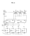
- FIG. 6 the application of the architecture shown in Fig. 4 to a 2K by 2K dual buffer image system is shown. It includes four memory blocks MO-M3, two deserializer modules 150 and 152, identical to that shown in Fig. 4 at 50.
- Oscillator 154 provides the clock frequency VCLK which is fed to a counter VCNT that divides the VCLK frequency in half.
- the VCLK/2 output is used as a clock for DSER modules 150 and 152.
- DSER module 150 generates the first four pixels and DSER module 152 generates the next four pixels, both at a frequency of VCLK/2.
- the pairs of consecutive pixel groups are further multiplexed by multiplexer 154, 156 and 158 which are also controlled by the VCLK/2 clock frequency.
- Output values from multiplexers 154, 156 and 158 are fed into digital-to-analog converters 160, 162 and 164 where the digital values are converted to analog values using the VCLK frequency.
- digital-to-analog converters 160, 162 and 164 serialize the outputs of DSER modules 150 and 152 while DSER modules 150 and 152 serialize the frame buffer outputs.
- the clock frequency used for the serializers within DSER modules 150 and 152 is generated by CNT 4 whose output is eight times slower than the VCLK signal.
- DSER modules 150 and 152 In operation, four 32 bit words are loaded into DSER modules 150 and 152, representing eight adjacent pixels in the horizontal row direction. Each row address stores two lines with 2K pixels in each and is video refreshed four times. The HCNT (1,0) bits still control what portions of the MASK data control the DSER modules for a particular line. As a result, 8K of video lines are stored in the frame buffer, providing dual 2K by 2K buffers with a video bandwidth equal to 8 times the serial clock frequency. If each memory module is constructed using two-4 megabit VRAM chips, the buffer uses only 8 chips. Using a conventional approach, the same buffer would take 64 four megabit chips.
Landscapes
- Engineering & Computer Science (AREA)
- Physics & Mathematics (AREA)
- Computer Hardware Design (AREA)
- General Physics & Mathematics (AREA)
- Theoretical Computer Science (AREA)
- Controls And Circuits For Display Device (AREA)
- Compression Of Band Width Or Redundancy In Fax (AREA)
Applications Claiming Priority (2)
| Application Number | Priority Date | Filing Date | Title |
|---|---|---|---|
| US73376891A | 1991-07-22 | 1991-07-22 | |
| US733768 | 1991-07-22 |
Publications (2)
| Publication Number | Publication Date |
|---|---|
| EP0525426A1 true EP0525426A1 (de) | 1993-02-03 |
| EP0525426B1 EP0525426B1 (de) | 1996-06-12 |
Family
ID=24949040
Family Applications (1)
| Application Number | Title | Priority Date | Filing Date |
|---|---|---|---|
| EP92111185A Expired - Lifetime EP0525426B1 (de) | 1991-07-22 | 1992-07-02 | Komprimierter Rasterbildspeicher für hochauflösende Rasteranzeige mit voller Farbwiedergabe |
Country Status (5)
| Country | Link |
|---|---|
| US (1) | US5430464A (de) |
| EP (1) | EP0525426B1 (de) |
| JP (1) | JPH0656546B2 (de) |
| DE (1) | DE69211435T2 (de) |
| SG (1) | SG46200A1 (de) |
Cited By (2)
| Publication number | Priority date | Publication date | Assignee | Title |
|---|---|---|---|---|
| WO1995030308A1 (en) * | 1994-04-29 | 1995-11-09 | Cirrus Logic, Inc. | Pcmcia video card |
| WO2006017405A3 (en) * | 2004-08-05 | 2006-04-13 | Hewlett Packard Development Co | Encoding image data using mask lookup table and decoding such encoded image data |
Families Citing this family (29)
| Publication number | Priority date | Publication date | Assignee | Title |
|---|---|---|---|---|
| US5585824A (en) * | 1991-07-22 | 1996-12-17 | Silicon Graphics, Inc. | Graphics memory apparatus and method |
| US5633661A (en) * | 1994-11-21 | 1997-05-27 | International Business Machines Corporation | Video display control system having block write with opaque pattern control expansion |
| JP3744018B2 (ja) * | 1995-02-09 | 2006-02-08 | ヤマハ株式会社 | ブロック画像シフト装置及び画像復号器 |
| US5689731A (en) * | 1995-06-07 | 1997-11-18 | International Business Machines Corporation | Programmable serializer using multiplexer and programmable address counter for providing flexiblity in scanning sequences and width of data |
| US5959637A (en) * | 1995-06-23 | 1999-09-28 | Cirrus Logic, Inc. | Method and apparatus for executing a raster operation in a graphics controller circuit |
| US5764963A (en) * | 1995-07-07 | 1998-06-09 | Rambus, Inc. | Method and apparatus for performing maskable multiple color block writes |
| US5760784A (en) * | 1996-01-22 | 1998-06-02 | International Business Machines Corporation | System and method for pacing the rate of display of decompressed video data |
| US5987169A (en) * | 1997-08-27 | 1999-11-16 | Sharp Laboratories Of America, Inc. | Method for improving chromatic text resolution in images with reduced chromatic bandwidth |
| JPH11109911A (ja) * | 1997-09-30 | 1999-04-23 | Fuurie Kk | 表示装置 |
| US6775417B2 (en) | 1997-10-02 | 2004-08-10 | S3 Graphics Co., Ltd. | Fixed-rate block-based image compression with inferred pixel values |
| JP3990783B2 (ja) * | 1997-11-14 | 2007-10-17 | キヤノン株式会社 | 画像処理装置及び画像処理方法 |
| US6573901B1 (en) | 2000-09-25 | 2003-06-03 | Seiko Epson Corporation | Video display controller with improved half-frame buffer |
| US7903892B2 (en) * | 2002-10-29 | 2011-03-08 | Ati Technologies Ulc | Image analysis for image compression suitability and real-time selection |
| JP4050605B2 (ja) * | 2002-12-13 | 2008-02-20 | 株式会社ルネサステクノロジ | 表示制御装置およびナビゲーションシステム |
| US8111928B2 (en) * | 2003-02-13 | 2012-02-07 | Ati Technologies Ulc | Method and apparatus for compression of multi-sampled anti-aliasing color data |
| US7764833B2 (en) * | 2003-02-13 | 2010-07-27 | Ati Technologies Ulc | Method and apparatus for anti-aliasing using floating point subpixel color values and compression of same |
| US7643679B2 (en) * | 2003-02-13 | 2010-01-05 | Ati Technologies Ulc | Method and apparatus for block based image compression with multiple non-uniform block encodings |
| US7202872B2 (en) * | 2003-10-29 | 2007-04-10 | Via Technologies, Inc. | Apparatus for compressing data in a bit stream or bit pattern |
| US7884861B2 (en) * | 2005-03-22 | 2011-02-08 | Microview Technologies PTD Ltd. | Image resolution multiplier |
| US7606429B2 (en) * | 2005-03-25 | 2009-10-20 | Ati Technologies Ulc | Block-based image compression method and apparatus |
| US7505624B2 (en) * | 2005-05-27 | 2009-03-17 | Ati Technologies Ulc | Block-based image compression method and apparatus |
| US8803857B2 (en) * | 2011-02-10 | 2014-08-12 | Ronald S. Cok | Chiplet display device with serial control |
| CN103108197A (zh) | 2011-11-14 | 2013-05-15 | 辉达公司 | 一种用于3d视频无线显示的优先级压缩方法和系统 |
| US9829715B2 (en) | 2012-01-23 | 2017-11-28 | Nvidia Corporation | Eyewear device for transmitting signal and communication method thereof |
| US9105250B2 (en) * | 2012-08-03 | 2015-08-11 | Nvidia Corporation | Coverage compaction |
| US9578224B2 (en) | 2012-09-10 | 2017-02-21 | Nvidia Corporation | System and method for enhanced monoimaging |
| US9002125B2 (en) | 2012-10-15 | 2015-04-07 | Nvidia Corporation | Z-plane compression with z-plane predictors |
| US10935788B2 (en) | 2014-01-24 | 2021-03-02 | Nvidia Corporation | Hybrid virtual 3D rendering approach to stereovision |
| US9906981B2 (en) | 2016-02-25 | 2018-02-27 | Nvidia Corporation | Method and system for dynamic regulation and control of Wi-Fi scans |
Citations (5)
| Publication number | Priority date | Publication date | Assignee | Title |
|---|---|---|---|---|
| WO1984002026A1 (en) * | 1982-11-16 | 1984-05-24 | Real Time Design Inc | Color video system using data compression and decompression |
| US4591842A (en) * | 1983-05-26 | 1986-05-27 | Honeywell Inc. | Apparatus for controlling the background and foreground colors displayed by raster graphic system |
| EP0279229A2 (de) * | 1987-02-12 | 1988-08-24 | International Business Machines Corporation | Grafik-Anzeigesystem |
| US4797729A (en) * | 1988-02-05 | 1989-01-10 | Eastman Kodak Company | System incorporating an error tolerant picture compression algorithm |
| US4893114A (en) * | 1985-06-10 | 1990-01-09 | Ascii Corporation | Image data processing system |
Family Cites Families (43)
| Publication number | Priority date | Publication date | Assignee | Title |
|---|---|---|---|---|
| JPS6031423B2 (ja) * | 1979-08-17 | 1985-07-22 | 富士通株式会社 | 圧縮デ−タ復元方式 |
| US4564915A (en) * | 1980-04-11 | 1986-01-14 | Ampex Corporation | YIQ Computer graphics system |
| JPS5776649A (en) * | 1980-10-31 | 1982-05-13 | Toshiba Corp | Picture information display device |
| US4410965A (en) * | 1981-09-18 | 1983-10-18 | Ncr Corporation | Data decompression apparatus and method |
| US4559535A (en) * | 1982-07-12 | 1985-12-17 | Sigmatron Nova, Inc. | System for displaying information with multiple shades of a color on a thin-film EL matrix display panel |
| US4639721A (en) * | 1982-10-09 | 1987-01-27 | Sharp Kabushiki Kaisha | Data selection circuit for the screen display of data from a personal computer |
| US4580134A (en) * | 1982-11-16 | 1986-04-01 | Real Time Design, Inc. | Color video system using data compression and decompression |
| US4626929A (en) * | 1983-03-15 | 1986-12-02 | Victor Company Of Japan, Ltd. | Color video signal recording and reproducing apparatus |
| US4541010A (en) * | 1983-06-17 | 1985-09-10 | Polaroid Corporation | Electronic imaging camera |
| US4654484A (en) * | 1983-07-21 | 1987-03-31 | Interand Corporation | Video compression/expansion system |
| US5163024A (en) * | 1983-12-30 | 1992-11-10 | Texas Instruments Incorporated | Video display system using memory with parallel and serial access employing serial shift registers selected by column address |
| JPS60247692A (ja) * | 1984-05-24 | 1985-12-07 | 株式会社 アスキ− | デイスプレイコントロ−ラ |
| US4683555A (en) * | 1985-01-22 | 1987-07-28 | Texas Instruments Incorporated | Serial accessed semiconductor memory with reconfigureable shift registers |
| CA1262969A (en) * | 1985-06-25 | 1989-11-14 | Ascii Corporation | Memory system |
| US4698788A (en) * | 1985-07-01 | 1987-10-06 | Motorola, Inc. | Memory architecture with sub-arrays |
| US4965845A (en) * | 1985-09-05 | 1990-10-23 | Harris Corporation | Compression and reconstruction of color aeronautical chart images |
| US4920504A (en) * | 1985-09-17 | 1990-04-24 | Nec Corporation | Display managing arrangement with a display memory divided into a matrix of memory blocks, each serving as a unit for display management |
| US5056041A (en) * | 1986-12-31 | 1991-10-08 | Texas Instruments Incorporated | Data processing apparatus with improved bit masking capability |
| IL77840A (en) * | 1986-02-10 | 1989-05-15 | Elscint Ltd | Data compression system for digital imaging |
| JPS62195982A (ja) * | 1986-02-24 | 1987-08-29 | Konishiroku Photo Ind Co Ltd | カラ−画像デ−タの圧縮方法及びその再生方法 |
| GB2188759B (en) * | 1986-04-05 | 1990-09-05 | Burr Brown Ltd | Data processing with op code early comparison |
| GB2189106B (en) * | 1986-04-14 | 1990-02-14 | Philips Electronic Associated | Image display |
| GB2190560B (en) * | 1986-05-08 | 1990-06-20 | Gen Electric Plc | Data compression |
| JPS6358395A (ja) * | 1986-08-11 | 1988-03-14 | テクトロニックス・インコ−ポレイテッド | カラ−表示装置 |
| GB2199461B (en) * | 1986-12-24 | 1991-03-13 | Philips Electronic Associated | Image display apparatus |
| US4772956A (en) * | 1987-06-02 | 1988-09-20 | Eastman Kodak Company | Dual block still video compander processor |
| EP0309884A3 (de) * | 1987-09-28 | 1991-04-10 | Mitsubishi Denki Kabushiki Kaisha | Farbbildanzeigegerät |
| US4941193A (en) * | 1987-10-02 | 1990-07-10 | Iterated Systems, Inc. | Methods and apparatus for image compression by iterated function system |
| US4897717A (en) * | 1988-03-30 | 1990-01-30 | Starsignal, Inc. | Computer-based video compression system |
| US4857993A (en) * | 1988-04-27 | 1989-08-15 | Universal Video Communications Corp. | Method and system for decompressing digital color video statistically encoded data |
| US4847677A (en) * | 1988-04-27 | 1989-07-11 | Universal Video Communications Corp. | Video telecommunication system and method for compressing and decompressing digital color video data |
| US4821119A (en) * | 1988-05-04 | 1989-04-11 | Bell Communications Research, Inc. | Method and apparatus for low bit-rate interframe video coding |
| JPH0221490A (ja) * | 1988-07-07 | 1990-01-24 | Oki Electric Ind Co Ltd | ダイナミック・ランダム・アクセス・メモリ |
| US5068650A (en) * | 1988-10-04 | 1991-11-26 | Bell Communications Research, Inc. | Memory system for high definition television display |
| US4975771A (en) * | 1989-02-10 | 1990-12-04 | Kassatly Salim A | Method and apparatus for TV broadcasting |
| US5148523A (en) * | 1988-11-29 | 1992-09-15 | Solbourne Computer, Inc. | Dynamic video RAM incorporationg on chip line modification |
| JP2796329B2 (ja) * | 1989-02-08 | 1998-09-10 | 株式会社日立製作所 | 表示メモリとそれを備えた画像処理装置 |
| GB2229059B (en) * | 1989-03-07 | 1993-08-04 | Sony Corp | Obtaining access to a two-dimensional portion of a digital picture signal |
| US4970663A (en) * | 1989-04-28 | 1990-11-13 | Avid Technology, Inc. | Method and apparatus for manipulating digital video data |
| DE69029065T2 (de) * | 1989-07-28 | 1997-03-06 | Texas Instruments Inc | Logische Schaltung und Verfahren zum Wiederordnen für einen graphischen Videoanzeigespeicher |
| US5138303A (en) * | 1989-10-31 | 1992-08-11 | Microsoft Corporation | Method and apparatus for displaying color on a computer output device using dithering techniques |
| US4985871A (en) * | 1989-11-13 | 1991-01-15 | Chips And Technologies, Inc. | Memory controller for using reserved dram addresses for expanded memory space |
| US5261049A (en) * | 1991-07-22 | 1993-11-09 | International Business Machines Corporation | Video RAM architecture incorporating hardware decompression |
-
1992
- 1992-06-05 JP JP4145465A patent/JPH0656546B2/ja not_active Expired - Lifetime
- 1992-07-02 SG SG1996000481A patent/SG46200A1/en unknown
- 1992-07-02 DE DE69211435T patent/DE69211435T2/de not_active Expired - Fee Related
- 1992-07-02 EP EP92111185A patent/EP0525426B1/de not_active Expired - Lifetime
-
1993
- 1993-12-22 US US08/173,137 patent/US5430464A/en not_active Expired - Fee Related
Patent Citations (5)
| Publication number | Priority date | Publication date | Assignee | Title |
|---|---|---|---|---|
| WO1984002026A1 (en) * | 1982-11-16 | 1984-05-24 | Real Time Design Inc | Color video system using data compression and decompression |
| US4591842A (en) * | 1983-05-26 | 1986-05-27 | Honeywell Inc. | Apparatus for controlling the background and foreground colors displayed by raster graphic system |
| US4893114A (en) * | 1985-06-10 | 1990-01-09 | Ascii Corporation | Image data processing system |
| EP0279229A2 (de) * | 1987-02-12 | 1988-08-24 | International Business Machines Corporation | Grafik-Anzeigesystem |
| US4797729A (en) * | 1988-02-05 | 1989-01-10 | Eastman Kodak Company | System incorporating an error tolerant picture compression algorithm |
Cited By (5)
| Publication number | Priority date | Publication date | Assignee | Title |
|---|---|---|---|---|
| WO1995030308A1 (en) * | 1994-04-29 | 1995-11-09 | Cirrus Logic, Inc. | Pcmcia video card |
| US5642139A (en) * | 1994-04-29 | 1997-06-24 | Cirrus Logic, Inc. | PCMCIA video card |
| US6023266A (en) * | 1994-04-29 | 2000-02-08 | Cirrus Logic, Inc. | PCMCIA video card |
| WO2006017405A3 (en) * | 2004-08-05 | 2006-04-13 | Hewlett Packard Development Co | Encoding image data using mask lookup table and decoding such encoded image data |
| US7551773B2 (en) | 2004-08-05 | 2009-06-23 | Hewlett-Packard Development Company, L.P. | Encoding image data using mask lookup table and decoding such encoded image data |
Also Published As
| Publication number | Publication date |
|---|---|
| DE69211435T2 (de) | 1996-12-05 |
| US5430464A (en) | 1995-07-04 |
| SG46200A1 (en) | 1998-02-20 |
| JPH05199419A (ja) | 1993-08-06 |
| JPH0656546B2 (ja) | 1994-07-27 |
| DE69211435D1 (de) | 1996-07-18 |
| EP0525426B1 (de) | 1996-06-12 |
Similar Documents
| Publication | Publication Date | Title |
|---|---|---|
| EP0525426B1 (de) | Komprimierter Rasterbildspeicher für hochauflösende Rasteranzeige mit voller Farbwiedergabe | |
| US4821208A (en) | Display processors accommodating the description of color pixels in variable-length codes | |
| US4823120A (en) | Enhanced video graphics controller | |
| US5367318A (en) | Method and apparatus for the simultaneous display of one or more selected images | |
| US6064404A (en) | Bandwidth and frame buffer size reduction in a digital pulse-width-modulated display system | |
| US5559954A (en) | Method & apparatus for displaying pixels from a multi-format frame buffer | |
| US5473342A (en) | Method and apparatus for on-the-fly multiple display mode switching in high-resolution bitmapped graphics system | |
| US5517612A (en) | Device for scaling real-time image frames in multi-media workstations | |
| US5933154A (en) | Multi-panel video display control addressing of interleaved frame buffers via CPU address conversion | |
| US4862154A (en) | Image display processor for graphics workstation | |
| US4991122A (en) | Weighted mapping of color value information onto a display screen | |
| US5469190A (en) | Apparatus for converting twenty-four bit color to fifteen bit color in a computer output display system | |
| US5012163A (en) | Method and apparatus for gamma correcting pixel value data in a computer graphics system | |
| CA2067418C (en) | Frame buffer organization and control for real-time image decompression | |
| EP0752695A2 (de) | Verfahren und Einrichtung zur gleichzeitigen Darstellung von Grafik und Videosignalen auf einem Rechnerbildschirm | |
| WO1995030308A1 (en) | Pcmcia video card | |
| JPS60178492A (ja) | 画素デ−タ表示方法 | |
| US5261049A (en) | Video RAM architecture incorporating hardware decompression | |
| US5625386A (en) | Method and apparatus for interleaving display buffers | |
| US5420609A (en) | Frame buffer, systems and methods | |
| US5230064A (en) | High resolution graphic display organization | |
| US4727423A (en) | Video data processing circuit employing plural parallel-to-serial converters and look-up tables | |
| US5065149A (en) | Scanned document image resolution enhancement | |
| JPH07240891A (ja) | 空間光変調器を用いた表示装置のためのディジタル・メモリ | |
| US5929868A (en) | Method and apparatus for computer display memory management |
Legal Events
| Date | Code | Title | Description |
|---|---|---|---|
| PUAI | Public reference made under article 153(3) epc to a published international application that has entered the european phase |
Free format text: ORIGINAL CODE: 0009012 |
|
| AK | Designated contracting states |
Kind code of ref document: A1 Designated state(s): DE FR GB |
|
| 17P | Request for examination filed |
Effective date: 19930519 |
|
| 17Q | First examination report despatched |
Effective date: 19950221 |
|
| GRAH | Despatch of communication of intention to grant a patent |
Free format text: ORIGINAL CODE: EPIDOS IGRA |
|
| GRAH | Despatch of communication of intention to grant a patent |
Free format text: ORIGINAL CODE: EPIDOS IGRA |
|
| GRAA | (expected) grant |
Free format text: ORIGINAL CODE: 0009210 |
|
| AK | Designated contracting states |
Kind code of ref document: B1 Designated state(s): DE FR GB |
|
| REF | Corresponds to: |
Ref document number: 69211435 Country of ref document: DE Date of ref document: 19960718 |
|
| ET | Fr: translation filed | ||
| ET | Fr: translation filed | ||
| PLBE | No opposition filed within time limit |
Free format text: ORIGINAL CODE: 0009261 |
|
| STAA | Information on the status of an ep patent application or granted ep patent |
Free format text: STATUS: NO OPPOSITION FILED WITHIN TIME LIMIT |
|
| 26N | No opposition filed | ||
| PGFP | Annual fee paid to national office [announced via postgrant information from national office to epo] |
Ref country code: GB Payment date: 19970625 Year of fee payment: 6 |
|
| PGFP | Annual fee paid to national office [announced via postgrant information from national office to epo] |
Ref country code: FR Payment date: 19970707 Year of fee payment: 6 |
|
| PGFP | Annual fee paid to national office [announced via postgrant information from national office to epo] |
Ref country code: DE Payment date: 19970725 Year of fee payment: 6 |
|
| PG25 | Lapsed in a contracting state [announced via postgrant information from national office to epo] |
Ref country code: GB Free format text: LAPSE BECAUSE OF NON-PAYMENT OF DUE FEES Effective date: 19980702 |
|
| GBPC | Gb: european patent ceased through non-payment of renewal fee |
Effective date: 19980702 |
|
| PG25 | Lapsed in a contracting state [announced via postgrant information from national office to epo] |
Ref country code: FR Free format text: LAPSE BECAUSE OF NON-PAYMENT OF DUE FEES Effective date: 19990331 |
|
| PG25 | Lapsed in a contracting state [announced via postgrant information from national office to epo] |
Ref country code: DE Free format text: LAPSE BECAUSE OF NON-PAYMENT OF DUE FEES Effective date: 19990501 |
|
| REG | Reference to a national code |
Ref country code: FR Ref legal event code: ST |