EP0525666B1 - Dispositif de traitement d'information incorporant un tampon de cible d'instruction de branchement - Google Patents
Dispositif de traitement d'information incorporant un tampon de cible d'instruction de branchement Download PDFInfo
- Publication number
- EP0525666B1 EP0525666B1 EP92112682A EP92112682A EP0525666B1 EP 0525666 B1 EP0525666 B1 EP 0525666B1 EP 92112682 A EP92112682 A EP 92112682A EP 92112682 A EP92112682 A EP 92112682A EP 0525666 B1 EP0525666 B1 EP 0525666B1
- Authority
- EP
- European Patent Office
- Prior art keywords
- instruction
- branch
- address
- bus
- address information
- Prior art date
- Legal status (The legal status is an assumption and is not a legal conclusion. Google has not performed a legal analysis and makes no representation as to the accuracy of the status listed.)
- Expired - Lifetime
Links
Images


Classifications
-
- G—PHYSICS
- G06—COMPUTING OR CALCULATING; COUNTING
- G06F—ELECTRIC DIGITAL DATA PROCESSING
- G06F9/00—Arrangements for program control, e.g. control units
- G06F9/06—Arrangements for program control, e.g. control units using stored programs, i.e. using an internal store of processing equipment to receive or retain programs
- G06F9/30—Arrangements for executing machine instructions, e.g. instruction decode
- G06F9/38—Concurrent instruction execution, e.g. pipeline or look ahead
- G06F9/3802—Instruction prefetching
- G06F9/3808—Instruction prefetching for instruction reuse, e.g. trace cache, branch target cache
-
- G—PHYSICS
- G06—COMPUTING OR CALCULATING; COUNTING
- G06F—ELECTRIC DIGITAL DATA PROCESSING
- G06F9/00—Arrangements for program control, e.g. control units
- G06F9/06—Arrangements for program control, e.g. control units using stored programs, i.e. using an internal store of processing equipment to receive or retain programs
- G06F9/30—Arrangements for executing machine instructions, e.g. instruction decode
-
- G—PHYSICS
- G06—COMPUTING OR CALCULATING; COUNTING
- G06F—ELECTRIC DIGITAL DATA PROCESSING
- G06F9/00—Arrangements for program control, e.g. control units
- G06F9/06—Arrangements for program control, e.g. control units using stored programs, i.e. using an internal store of processing equipment to receive or retain programs
- G06F9/30—Arrangements for executing machine instructions, e.g. instruction decode
- G06F9/38—Concurrent instruction execution, e.g. pipeline or look ahead
- G06F9/3861—Recovery, e.g. branch miss-prediction, exception handling
Definitions
- the present invention relates to an information processing apparatus and, more particularly, to an improvement in a microcomputer as an information processing apparatus which must fetch an instruction at a branch address in order to change an instruction stream.
- a microcomputer executes instructions in a current instruction stream in order, it is often required to change the current instruction stream in response to a conditional/unconditional branch instruction (called collectively a "branch instruction”) or an interrupt request.
- the microcomputer has to perform a bus cycle to fetch an instruction at a branch address of a main memory from which a new instruction stream starts.
- An instruction at a branch address will be called hereinafter a "branch target instruction".
- Some microcomputers include a branch prediction unit. This unit operates to detect the prefetching of the branch instruction, obtain a branch address, and then cause the prefetch unit to prefetch an instruction at that branch address (i.e., a branch target instruction) before the execution unit executes the branch instruction.
- a branch target instruction i.e., a branch target instruction
- the execution unit receives and executes the branch target instruction which has already been fetched in the microcomputer.
- the bus cycle for fetching the branch target instruction is performed as an instruction prefetching operation and does not suspend the data processing operation of the microcomputer.
- a bus cycle for fetching an instruction following the branch instruction is required to invalidate the prefetched branch target instruction.
- This bus cycle causes temporary suspension of the data operation of the microcomputer.
- the branch prediction unit does not answer the branch request responsive to the interrupt request.
- a bus cycle for fetching a branch target instruction for an interrupt subroutine program, which is performed after suspending the current program execution, is required each time the interrupt request occurs.
- Some microcomputers further incorporate a cache memory for copying a string of instructions and/or data stored in the main memory.
- a cache memory for copying a string of instructions and/or data stored in the main memory.
- that instruction is read out therefrom and transferred to the execution unit at a high speed, one clock for example, in response to the branch request.
- the cache memory copies only instructions stored in addresses which are in the neighborhood of the address storing the instruction being currently executed.
- the branch target instruction required is not always stored in the cache memory.
- Fig. 9 is a block diagram of a conventional microcomputer which includes an instruction cache.
- This structure incorporates a bus controller unit 620, an execution unit 630, an external data bus terminal 640, an internal bus 650, a cache controller unit 660, an instruction cache 670, and an instruction bus 680.
- the bus controller unit 620 which is connected to the internal bus 650, receives a fetch request signal 651 from the cache controller unit 660.
- the bus controller unit 620 controls data reading and writing to and from an on-chip or off-chip memory (not shown), and also control input/output (I/O) operation.
- the bus controller unit 620 further controls fetching of instruction code stored in a memory (not shown).
- the execution unit 630 connected to the internal bus 650 and instruction bus 680, outputs an instruction signal 652 to the cache controller unit 660.
- the execution unit 630 also decodes the instruction code supplied from the instruction bus 680 and controls execution logical and data transfer operations.
- the external bus terminal 640 which is connected to the internal bus 650, is a 16-bit terminal.
- the internal bus 650 is 16 bits wide and, in addition to be connected to the external bus terminal 640, also is connected to the bus controller unit 620, the execution unit 630, and the instruction cache 670.
- the cache controller unit 660 which is connected to the bus controller unit 620, the execution unit 630, and the instruction cache 670, outputs a write signal 653 for writing an instruction code to the instruction cache 670.
- the cache controller unit 660 also commands the instruction cache 670 to output the instruction code in response to the instruction request signal 652 supplied from the execution unit 630.
- the instruction cache 670 connected to the internal bus 650, the cache controller unit 660, and the instruction bus 680, is responsive to the write signal 653 from the cache controller unit 660 to store an instruction code on the internal bus 650, and the address from which the instruction code has been read. If the cache controller 660 does not issue the write signal 653, the cache 670 outputs the stored instruction code on bus 680.
- the instruction bus 680 connected to the instruction cache 670 and the execution unit 630, sends the instruction code stored in the instruction cache 670 to the execution unit 630.
- the microcomputer of Fig. 9 operates as follows.
- the execution unit 630 outputs the instruction request signal 652 to the cache controller unit 660, which compares the address information stored in the instruction cache 670 with an address generated in the bus controller unit 620. If there is coincidence (a condition known generally as a "cache hit"), the instruction code is supposed from the instruction cache 670 to the instruction bus 680. Since the instruction cache generally is comprised of high speed memory, the execution unit 630 can read and execute an instruction code at every clock cycle from the instruction bus 680 when there is a cache hit.
- the cache controller unit 660 recognizes that the requested instruction code does not exist in the instruction cache 670, and supplies the fetch request signal 651 to the bus controller unit 620.
- the bus controller unit 620 starts a bus cycle for reading an instruction code from the main memory (not shown) through the external data bus terminal 640 and the internal bus 650.
- the cache controller unit 660 outputs a write signal 653, so that the read instruction code and address information from which the code is read are written into the instruction cache 670, and the instruction code applied simultaneously to the instruction bus 680. Until the bus cycle terminates, say after three clock periods, instruction code is not supplied to the execution unit 630, so that instruction execution is inhibited.
- the cache controller unit 660 also starts a write cycle for reading an instruction code, stored in main memory at an address equal to the address information stored in the instruction cache 670, and then writing that information to the instruction cache 670 through the data terminal 640 and the internal bus 650.
- cache memory structure is relatively complicated.
- cache operation is a statistical process; hence the need to take up precious bus cycles for fetches in the event of a cache miss.
- the statistical aspect of cache operation in the context of the handling of branch instructions becomes more apparent in view of branch target instruction decoding operations, which also were mentioned earlier.
- branch target instruction decoding operations which also were mentioned earlier.
- the various prefetches include the prefetch of an unconditional branch (i.e. a branch that is always taken); the prefetch of a conditional branch using a prediction bit, and a prefetch of a branch address indication through an indirect address stored in a register.
- the usual capacity of cache included in a large scale integration (LSI) chip is 32 pages of 16 bytes each. Though execution of instruction code at successive addresses, or the branch inside the page can be processed at high speed, the branch outside the page occurs often in the control field, where there are many branches, and there is a need to update the cache frequently.
- the cache size could be increased to 64 pages of 32 bytes each, but this requires an increase in chip area, with an unacceptable attendant increase in product cost, particularly in the control area. Even if an instruction cache were provided external to the microcomputer chip, an additional bus only for the cache, and cache control terminals are necessary, resulting in a larger LSI package size.
- the prefetching of instructions at the branch target address requires an additional instruction decoder in the prefetch queue, and a buffer circuit for storing prefetched data.
- the prefetch function can process only branch instructions, but not interrupts, which also occur frequently in the control field.
- the more complicated hardware cannot handle all of the situations which can occur.
- the statistical nature of the operation of the cache-based circuitry can result in the waste of precious bus cycles, and the necessity of flushing of the cache, when branches are not taken.
- EP-A-0,179,245 discloses an architecture for small instruction caches.
- a branch target table is used as an instruction memory which is referenced by the addresses of instructions which are targets of branches.
- the branch target table consists of a target address table, a next fetch address table, a valid entries table and an instruction table.
- some of the bits in the untranslated part of the address of the target instruction, i.e. the instruction being branched to, are used to address a line of the branch target table.
- all entries of the branch target table line are accessed, and the translated address is compared to the target address table entry on that line.
- the instruction prefetch unit fetches the instruction addressed by the next fetch address table entry for the given line and the line of instructions associated with the branch address table entry is read into an instruction queue having a length set by the valid entry table entry which indicates how many of these instructions are valid. Otherwise, the instruction prefetch unit fetches the target and subsequent instructions as it would if there were no branch target table, and the target address table entry is set to the real address of the target instruction.
- the next fetch address table is updated so that it always contains the address of the instruction which follows the last valid instruction in the line, and the valid entries table is updated so that it always counts the number of valid instructions in the line.
- EP-A-0,270,310 discloses methods and apparatus for giving access to instructions in computer systems. Methods and apparatus are set forth for optimizing the performance of instruction processors using an instruction cache memory in combination with a sequential transfer main memory.
- the novel memory system stores preselected instructions in cache memory. The instructions are those that immediately follow a branch operation. The purpose of storing these instructions is to minimize, and if possible, eliminate the delay associated with fetching the same sequence from main memory following a subsequent branch to the same instruction string.
- the number of instructions that need to be cached (placed in cache memory) is a function of the access time for the first and subsequent fetches from sequential main memory, the speed of the cache memory, and instruction execution time.
- the invention is particularly well suited for use in computer systems having RISC architectures with fixed instructions lengths.
- one object of the present invention is to provide an improved microcomputer.
- Another object of the present invention is to provide a microcomputer having improved data processing speed and/or efficiency.
- Still another object of the present invention is to provide a microcomputer in which each of a plurality of branch target instructions can be transferred to an execution unit at high speed.
- Still another object of the present invention is to provide a microcomputer in which a branch target instruction is supplied to an execution unit in one clock without needing complicated hardware.
- a microcomputer according to the present invention is defined in independent claim 1.
- the dependent claims define particular embodiments of the invention.
- a microcomputer is provided with a bus control unit performing a bus cycle for fetching an instruction from a memory and further performing a bus cycle for reading or writing data from or into the memory; an execution unit executing an instruction supplied thereto and issuing a branch request including address information representative of a branch address; and a branch target instruction buffer unit coupled to the bus control unit and the execution unit. Responsive to both the branch request from the execution unit and a control signal from the buffer unit, the bus control unit performs a bus cycle for fetching an instruction from the branch address of the memory and outputs the instruction as a branch target instruction.
- the buffer unit includes a plurality of storage buffers each, when written, temporarily storing address information and an instruction associated with the stored address information, a detection circuit responding to the branch request from the execution unit to produce a detection signal of an active level when any one of the storage buffers stores address information that is the same as the address information included in the branch request.
- the detection circuit produces a detection signal of an inactive level when none of the storage buffers stores the address information that is the same as the address information included in the branch request, the detection signal of the inactive level being supplied to the bus control unit as the control signal.
- a selection control circuit selects and supplies the instruction read out of the storage buffer to the execution unit in response to the active level of the detection signal and selects and supplies the branch target instruction outputted from the bus control unit to the execution unit in response to the inactive level of the detection signal.
- An information updating circuit responds to the inactive level of the detection signal to write into one storage buffer the branch target instruction and address information representative of the branch address.
- a branch target instruction to be fetched by the branch request responsive to the execution of a branch instruction or an interrupt request is held in the buffer unit, it is transferred immediately to the execution unit without performing a bus cycle for fetching the branch target instruction. If the required branch target instruction is not held, a bus cycle is required to fetch it. However, the fetched branch target instruction is held in the buffer unit. Therefore, the buffer unit can transfer the stored branch target instruction to the execution unit in response to the next or following branch request.
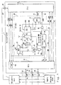
- a microcomputer 1 is fabricated on a single semiconductor chip as a 16-bit microcomputer and is interconnected to a memory 2 and a peripheral unit 3 via a system bus which includes a system data bus (SDB) 4, a system address bus (SAB) 5, and a system control bus (SCB) 6.
- the memory 2 stores a program and operand data.
- the SDB 4 is 16 bits wide.
- the SAB 5 is also 16 bits wide to support a 64K-byte address space.
- the SDB 4, SAB 5, and SCB 6 are connected respectively to a set of data terminals 41, a set of address terminals 42 and a set of control terminals 43 of the microcomputer 1.
- the microcomputer 1 also has an interrupt terminal 44 supplied with an interrupt request signal INT from the peripheral unit 3.
- the microcomputer 1 includes a bus control unit (BCU) 10 and an execution unit (EXU) 20 and further includes a branch target instruction buffer unit (BTIBU) 30 in accordance with the present invention.
- the BCU 10 and the EXU 20 are interconnected with each other via an internal bus consisting of a 16-bit wide internal data bus (IDB) 45, an internal address bus (IAB) 46, and an internal control bus (ICB) 47.
- IAB internal address bus
- ICB internal control bus
- the BCU 10 preforms a bus cycle for reading or writing operand data from or into the memory 2 or the peripheral unit 3.
- the EXU 20 further supplies to the BCU 10 a fetch request (FREQ) signal 48 to inform the BCU 10 of an instruction prefetch request and a branch request (BREQ) signal 49 to inform the BCU 10 of a branch request responsive to the execution of a branch instruction or an interrupt request.
- FREQ fetch request
- BREQ branch request
- the EXU 20 further supplies to the BCU 10 a 16-bit branch address via an instruction address bus (INA) 50.
- the BCU 10 includes an instruction prefetch pointer (FAP) 101 whose content indicates the address of the memory 2 from which an instruction is to be prefetched. Accordingly, the BCU performs a bus cycle for fetching an instruction from the memory 2, incrementing the content of the FAP 101 each time the FREQ signal 48 is generated from the EXU 20.
- FAP instruction prefetch pointer
- the branch address on the INA 50 is latched in the FAP 101. The BCU 10 then performs a bus cycle for fetching an instruction.
- Each of the bus cycles for fetching an instruction and for accessing to operand data consists of first to fourth states T1 to T4 (see, e.g. Fig. 3).
- a hit state TH is inserted at the beginning of the instruction fetch bus cycle consisting of the T1 to T4 states.
- Each of the states T1 to T4 and TH has a period of time corresponding to one clock cycle of a system clock signal (not showy) supplied to the microcomputer 1.
- the operand data read out of the memory 2 or the peripheral unit 3 are transferred through the SDB 4 and IDB 45 to the EXU 20.
- the instruction fetched from the memory 2 is transferred to the EXU 20 through SDB 4 and IDB 45 and further through a multiplexer (MPX) 37 in the BTIBU 30 and an instruction bus (INB) 51.
- the EXU 20 is notified of the appearance of the instruction on the INB 51 by an AQWE signal 53 which is outputted from an OR gate 38 in the BTIBU 30 receiving an instruction capture-enable signal (QWE) 52 produced by the BCU 10 and a multiplexer control signal MPC produced by a timing control circuit 36 in the BTIBU 30. That is, the EXU 20 captures the instruction on the INB 51 in response to the AQWE signal 53.
- the QWE signal 52 is generated in synchronism with the fourth state signal T4.
- the BTIBU 30 includes a branch address pointer (BAP) 31 which latches the branch address on the INA 50 in response to the BREQ signal 49.
- the branch address has 16 bits consisting of the 0th bit to the fifteenth bit, as mentioned before.
- the 0th bit is the least significant bit (LSB) and the fifteenth bit is the most significant bit (MSB).
- the first to fifth bits of the branch address latched in the BAP 31 are supplied to a decoder 33.
- This decoder 33 when activated by a decoding-enable signal DE supplied thereto, decodes the information represented by the supplied five bits and then energizes one of 32 selection lines coupled to a buffer 33. This means that the buffer 33 consists of 32 line buffers.
- Each of the line buffers has a one-bit valid flag storage area 321, a 10-bit branch address storage area 322 (for the sixth to fifteenth bits), and a 16-bit branch target instruction storage area 323. Since the area 323 is a 16-bit area, the 0th bit (LSB) of the latched branch address need not be supplied to the decoder 31.
- the buffer 32 is further supplied with a buffer write-enable signal BWE and a buffer read-enable signal BRE.
- BWE write-enable signal
- BRE buffer read-enable signal
- the comparator 34 has a set of second input terminals supplied with the sixth to fifteenth bits of the latched branch address and, when activated by an active high comparator-enable signal CE, compares the data supplied from the BAP 31 with that from the buffer 32. When the compared data are the same, the comparator 34 produces and supplies a high level output to a second input terminal of the AND gate 35 which further has a third input terminal supplied with a branch cycle signal BRC.
- the AND gate 35 changes the branch hit signal BRH to the active high level which is in turn supplied to the BCU 10 and a timing control circuit 36.
- This circuit 36 is further supplied with the branch request signal BREQ, the hit state signal TH, and the fourth state signal T4 and then produces the above-mentioned timing control signals BRC, DE, CE, BWE, BRE and MPC.
- the multiplexer control signal MPC is supplied to the MPX 37.
- the MPX 37 selects the data outputted from the buffer 32 when the signal MPC takes the high level and the data on the IDB 45 when the signal MPC takes the low level.
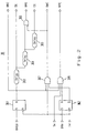
- the timing control circuit 36 includes two flip-flop circuits (F/Fs) 361 and 362, three delay circuits 363, 364, and 365, and four AND gates 366, 367, and 368 which are connected as shown. Operation of this structure will be described in detail below.
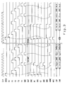
- the EXU 20 receives and executes each instruction supplied through the INB 51. Assume that the EXU 20 encounters a branch instruction having a branch address "0110H". The mark "H" indicates hexadecimal notation. As the result of the execution of the branch instruction, the EXU 20 supplies the branch address "0110H" onto the INA 50 while producing the BREQ signal 49 in synchronism with a system clock CLK, as shown in Fig. 3. In response to the BREQ signal 49, the BAP 31 and FAP 101 both latch the branch address "0110H". Further, the F/F 361 (Fig.
- the decoder 33 selects the eighth line buffer of the buffer 32.
- the flag area 321 of the buffer 32 is reset to zero upon the system reset, so that the flag information of the eighth line buffer is logic "0", as shown in Fig. 4A.
- the buffer read-enable signal BRE the logic "0" is read out of the flag area 321 and supplied to the AND gate 35. Therefore, the branch hit signal BRH outputted from the AND gate 35 is held at the inactive low level irrespective of the contents stored in the address area 322 of the eighth line buffer.
- the BCU 10 judges the instruction at the branch address "0110H" as not being stored in the buffer 32 and then initiates a bus cycle for fetching the branch target instruction.
- This bus cycle consists of four states T1 to T4, as shown in Fig. 3.
- the branch target instruction is thereby read out of the branch address of the memory 2 and supplied to the MPX 37 through the SDB 4 and IDB 45.
- the F/F 362 (Fig. 2) is maintained in the reset state to produce the low level Q output. Accordingly, the output of the AND gate 379, i.e. the multiplexer control signal MPC, is at the low level.
- the branch target instruction on the IDB 45 thus appears on the INB 51 trough the MPX 37, as shown in Fig. 3.
- the BCU 10 produces the instruction capture-enable signal QWE to cause the signal AQWE to change the active high level in synchronism with the fourth state signal T4.
- the EXU 20 captures and executes the branch target instruction.
- the AND gate 367 changes the buffer write-enable signal BWE to the active high level, whereas the buffer read-enable signal BRE is changed to the low level, as shown in Fig. 3.
- the eighth line buffer of the buffer 32 is written with and thus stores the logic "1" in the flag storage area 321, the address information of the sixth to fifteenth bits, "0000 0001 00B", of the branch address "0110H” in the address storage area 322, and the branch target instruction consisting of the one-byte instruction code at the address "0110H” and that at the address "0111H” in the instruction storage area 323, as shown in Fig. 4B.
- the F/F 361 is reset to change its output to the low level, so that the timing signals BRC, DE, CE and BWE are changed to the low level, as shown in Fig. 3.
- the BCU 10 Since the BCU 10 has performed the instruction fetch bus cycle responsive to the BREQ signal 49, it initiates consecutively the instruction fetch bus cycle at least twice by incrementing the content of the FAP 101 by two, as shown in Fig. 3. At this time, the F/F 361 is not set, so that the BTIBU 30 does not operate. That is, no instruction thus fetched thereafter is stored in the buffer 32. On the other hand, the EXU 20 executes in order the instructions in a new instruction stream starting from the branch target instruction at the branch address "0110H". As mentioned before, each time the EXU 20 produces the instruction prefetch request signal FREQ 48, the BCU 10 initiates the instruction fetch bus cycle by incrementing the content of the FAP 101 by two. The fetched instruction is transferred to the EXU 20 via the SDB 4, IDB 45, MPX 37, and INB 51.
- the peripheral unit 3 issues an interrupt request INT to the microcomputer 1.
- the EXU 20 suspends the execution of the current instruction stream in response to the interrupt request INT and then saves the internal status thereof into a stack area (not shown).
- the EXU 20 thereafter produces the branch request signal BREQ 49 while supplying onto the INA 50 a branch address indicating the starting address of an interrupt program for the interrupt request INT.
- the branch address is "5A83H”
- the decoder 33 responds to the first to fifth bits thereof, "000001B", to select the first line buffer of the buffer 32.
- the BCU 10 Since the flag data stored therein is the logic "0", the BCU 10 initiates the bus cycle to read a branch target instruction from the memory 2, which is in turn supplied to the EXU 20, as described before. The EXU 20 thus starts to execute the interrupt program.
- the branch target instruction is further written into the first line buffer of the buffer 32 together with the logic "1" flag and the branch address information from the sixth to fifteenth bits, "0101 1010 10B", as shown in Fig. 4C.
- the one-byte instruction code at the address "5A82H” and that at the address "5A83H" are stored in the instruction area 323 as the branch target instruction, because the BCU 10 reads one word (16 bits) as two bytes at a time from the memory 2.
- the BCU 10 then continues to perform the instruction fetch bus cycle at least twice, as mentioned before.
- the EXU 20 produces the branch request BREQ 49 while supplying the branch address "5A83H" onto the INA 50.
- the BAP 31 and the FAP 101 latch that address, and the F/F 361 (Fig. 2) is set to produce the high level output.
- the branch hit signal BRH is changed to the active high level.
- the high level of the BRH signal is supplied to the BCU 10 along with the BREQ signal, so that the BCU 10 generates the hit state signal TH before initiating the bus cycle, as shown in Fig. 3. Since the F/F 362 (Fig.
- the hit state signal TH causes the AND gate 368 to change the MPC signal to the high level.
- the MPX 37 thereby selects the first terminals at which the branch target instruction has already arrived from the buffer 32.
- the high MPC signal further changes the signal AQWE to the high level, as shown in Fig. 3.
- the branch target instruction responsive to the branch request caused by the interrupt request is transferred to the EXU 20 from the BTIBU 30 within one clock.
- this instruction code is disregarded since the EXU 20 knows the branch address, as well known in the art.
- the BCU 10 initiates the bus cycle following the hit state TH.
- the BCU 10 receives the high level branch hit signal BRH, so that the instruction fetch bus cycle operation is performed on an instruction at the address "5A84H" by incrementing the content of the FAP 101.
- This instruction is captured by the EXU 20 in the fourth state T4.
- the AND gate 367 does not change the buffer write-enable signal BWE to the active high level even when the state signal T4 appears, as shown in Fig. 3. No instruction is thereby written into the buffer 32.
- the BCU 10 continues to perform the instruction fetch bus cycle at least twice, as mentioned before.
- the BTIBU 30 each time the EXU 20 issues a branch request responsive to the execution of the branch instruction or the interrupt request INT, the BTIBU 30 checks whether or not a branch target instruction is stored in the buffer 32 and, if stored, transfers that instruction to the EXU 20 within one clock. If not stored, on the other hand, the BTIBU 30 causes the BCU 10 to initiate the bus cycle for fetching a branch target instruction and then stores the fetched instruction.
- the buffer 32 can store up to 32 branch target instructions.
- Some branch address is often the same as another branch address in its first to fifth bits.
- the EXU 20 issues another branch request with a branch address "1290H”.
- the first to fifth bits thereof are "01000B”
- the eighth line buffer of the buffer 32 is selected which stored the address information of "0000 0001 00B”.
- the sixth to fifteenth bits of the newly requested branch address are "0001 0010 10B”. Consequently, the AND gate 35 outputs the low level branch hit signal BRH.
- the BCU 10 thereby initiates the bus cycle for fetching the instruction at the address "1290H”.
- the fetched branch target instruction is transferred to the EXU 20 and further is written into the eighth line buffer together with the logic "1" flag and the address information of "0001 0010 10B".
- the eighth line buffer is thus updated.
- Fig. 5 shows a microcomputer system employing a microcomputer according to another embodiment of the present invention, in which the same elements as those shown in Fig. 1 are denoted by the same reference numerals, so that it is possible to omit further description thereof.
- This microcomputer is an 8-bit microcomputer, and thus a system data bus (SDB) and an internal data bus (IDB) both are 8-bit buses, as represented by the reference numerals 401 and 4501, respectively.
- the instruction bus (INB) 51 is 16 bits wide. Therefore, two one-byte prebuffers 503 and 504 are provided between the IDB 4501 and the MPX 37.
- the prebuffer 503 responds to a first prebuffer-enable signal PB1 to store and supply the information on the IDB 4501 to the less significant inputs of the MPX 37, whereas the prebuffer 504 responds to a second prebuffer-enable signal PB2 to store and supply the information on the IDB 4501 to the more significant inputs of the MPX 37.
- These signals PB1 and PB2 are generated by the timing control circuit 36.
- the signal PB2 is further supplied to the OR gate 38 in place of the signal AQWE which is supplied to the timing control circuit 36 in this embodiment.
- the BTIBU 30 further includes an inverter 501 supplied with the 0th bit of the address information latched in the BAP 31.
- the output of the inverter 501 is supplied in common to an even-number storage area provided newly to each of the line buffers 32.
- the input to the inverter 501 and the output of the storage area 324 are ORed by an OR gate 502 whose output is in turn supplied to the AND gate 35 as a fourth input signal.
- the timing control circuit 36 of the present microcomputer includes, in addition to the constituents shown in Fig. 2, one T-type flip-flop (TF/F) 3615, two delay circuits 3616 and 3617 and two AND gates 3618 and 3619 connected as shown to produce the prebuffer-enable signals PB1 and PB2. Further, the signal PB2 is supplied to the AND gate 367 in place of the state signal T4.
- T-type flip-flop T-type flip-flop
- the EXU 20 produces the branch request signal BREQ 48 with a branch address "29E5H" in response to the execution of a branch instruction or an interrupt request INT
- an 18th line buffer of the buffer 32 is selected by the decoder 33 in response to the first to fifth bits of the branch address, "10010B".
- the branch hit signal BRH is held at the low level, as shown in Fig. 7. Accordingly, the BCU 20 initiates the bus cycle for fetching a branch target instruction.
- the SDB 401 and the IDB 4501 are 8-bit buses, whereas the INB 51 is a 16-bit bus. Therefore, the BCU 20 performs the instruction fetch bus cycle twice consecutively. However, the BCU 20 generates the instruction capture-enable signal QWE in the fourth state T4 of each bus cycle.
- the T-F/F 3615, the delay circuit 3616 and the AND gate 3618 produces the first prebuffer-enable signal PB1 to cause the prebuffer 503 to store the instruction at the address "29E5H".
- the second prebuffer-enable signal PB2 is produced by the T-F/F 3615, the delay circuit 3617 and the AND gate 3619, so that the prebuffer 504 stores the instruction at the address "29E6H”.
- the second prebuffer-enable signal PB2 further changes the signal AQWE to the active high level.
- the multiplexer control signal MPC is held at the low level.
- the branch target instruction is transferred to the EXU 20 from the BCU 10, as shown in Fig. 7.
- the second prebuffer-enable signal PB2 further causes the AND gate 367 (Fig. 6) to produce the active buffer write-enable signal BWE since the F/F 362 is at the reset state.
- the 18th line buffer of the buffer 32 is written with and thus stores the inverted 0th bit of the branch address derived from the inverter 501, i.e. the logic "0", in the storage area 324, the logic "1" in the flag storage area 321, the sixth to fifteenth bits of the branch address, i.e. "0010 1001 11B", in the address storage area 322, and the two one-byte instruction codes at the address "29E5H" and "29E6H” in the storage area 323, as shown in Fig. 8B.
- the BCU 20 continues to perform the instruction fetch bus cycle at least four times to fetch four bytes of instruction codes, as shown in Fig. 7.
- the 18th line buffer of the buffer 32 is selected again, and the contents thereof are read out therefrom.
- the read-out flag is the logic "1”
- the read-out information from the area 324 is the logic "0”.
- the 0th bit of the branch address is also the logic "0”. Accordingly, the low level branch hit signal BRH is produced to cause the BCU 10 to initiate the instruction fetch bus cycle.
- Two one-byte instruction codes at the addresses "29E4H” and "29E5H” are thereby written into the 18th line buffer in the same manner as described hereinbefore, as shown in Fig. 8C.
- the storage area 324 is written with the inverted 0th bit of the branch address, i.e. the logic "1", however.
- the high level branch hit signal BRH is produced as shown in Fig. 7, because the 0th bit of the branch address and the data read out of the area 324 both are the logic "1".
- the control signal MPC is thereby changed to the high level to transfer to the EXU 20 the instruction codes at the addresses "29E4H” and "29E5H” within one clock, as shown in Fig. 7.
- the instruction code at the address "29E4H” is disregarded, however.
- the BCU 10 initiates the bus cycle for fetching the instruction codes the address "29E6H" by incrementing the content of the FAP 101. These instruction codes are not stored in the BTIBU 30, as mentioned before.
- the BTIBU 30 in the present embodiment can store up to 64 branch target instructions.
- the branch target instruction to be stored is updated when the first to fifth bits of the new branch address are the same as those of the stored branch address but the remaining bits are different from each other.
Landscapes
- Engineering & Computer Science (AREA)
- Software Systems (AREA)
- Theoretical Computer Science (AREA)
- Physics & Mathematics (AREA)
- General Engineering & Computer Science (AREA)
- General Physics & Mathematics (AREA)
- Advance Control (AREA)
- Executing Machine-Instructions (AREA)
Claims (5)
- Microprocesseur comportant :ladite unité tampon d'instruction cible de branchement (30) comportant :une unité de commande de bus (10) effectuant un cycle de bus pour lire une instruction et délivrer en sortie ladite instruction lue dans un bus (45),une unité d'exécution (20) exécutant une instruction envoyée dans celle-ci et émettant une demande de branchement comportant des informations d'adresse de branchement représentatives d'une adresse de branchement, etune unité tampon d'instruction cible de branchement (30) reliée à ladite unité de commande de bus (10) et à ladite unité d'exécution (20), ladite unité de commande de bus (10) étant sensible à la fois à ladite demande de branchement provenant de ladite unité d'exécution (20) et à un signal de commande provenant de ladite unité tampon d'instruction cible de branchement (30) pour initialiser le cycle de bus afin de lire une instruction depuis ladite adresse de branchement pour émettre ainsi une instruction cible de branchement,caractérisé parune pluralité de tampons de mémorisation (32) pour mémoriser temporairement des informations d'adresse et une instruction associée aux informations d'adresse mémorisées,un circuit de détection (34, 35), sensible à ladite demande de branchement, pour produire un signal de détection ayant un niveau actif lorsqu'un quelconque desdits tampons de mémorisation (32) mémorise les informations d'adresse qui sont les mêmes que les informations d'adresse provenant de ladite unité d'exécution, et un signal de détection ayant un niveau inactif lorsqu'aucun desdits tampons de mémorisation (32) mémorise les informations d'adresse qui sont les mêmes que les informations d'adresse provenant de ladite unité d'exécution (20), ledit niveau actif dudit signal de détection et ledit niveau inactif dudit signal de détection étant envoyés dans ladite unité de commande de bus en tant que ledit signal de commande,un circuit de commande de sélection (37) pour sélectionner l'instruction lue à partir d'un desdits tampons de mémorisation (32) et envoyer celle-ci dans ladite unité d'exécution (20) en réponse audit niveau actif dudit signal de détection, et sélectionner ladite instruction cible de branchement lue sur ledit bus (45) et envoyer celle-ci dans ladite unité d'exécution (20) en réponse audit niveau inactif dudit signal de détection, etune unité de mise à jour d'informations (36) pour écrire ladite instruction cible de branchement et les informations d'adresse associées à celle-ci dans un desdits tampons de mémorisation (32) en réponse audit niveau inactif dudit signal de détection,ledit circuit de commande de bus (10) ayant un pointeur d'adresse de lecture (101) pour mémoriser ladite adresse de branchement en réponse à ladite demande de branchement et délivrer en sortie une adresse suivante dans une unité périphérique (2, 3), l'adresse suivante étant produite en incrémentant ladite adresse de branchement en réponse audit niveau inactif dudit signal de détection, pour lire une instruction provenant de ladite unité périphérique (2, 3) en réponse à ladite adresse suivante dans ledit bus (45).
- Micro-ordinateur selon la revendication 1, dans lequel chacune desdites informations d'adresse dans lesdits tampons de mémorisation (32) a une première et une seconde partie et chacun desdits tampons de mémorisation (32) mémorise ladite seconde partie des informations d'adresse, ledit circuit de détection (34, 35) comportant un décodeur (32) qui est sensible à ladite première partie des informations d'adresse provenant de ladite unité d'exécution pour sélectionner un desdits tampons de mémorisation et un comparateur (34) comparant ladite seconde partie des informations d'adresse provenant de ladite unité d'exécution à la seconde partie des informations d'adresse lues à partir du tampon de mémorisation sélectionné pour produire ledit signal de détection.
- Micro-ordinateur selon la revendication 1, dans lequel ledit circuit de sélection (37) comporte un multiplexeur (37) ayant une borne de commande alimentée par ledit signal de détection, un ensemble de premières bornes reliées auxdits tampons de mémorisation (32) pour recevoir l'instruction de ceux-ci et un ensemble de secondes bornes reliées à ladite unité de commande de bus pour recevoir l'instruction de celle-ci, ledit multiplexeur sélectionnant lesdites premières bornes en réponse audit niveau actif dudit signal de détection et ladite seconde borne en réponse audit niveau inactif dudit signal de détection.
- Micro-ordinateur selon la revendication 1, dans lequel ladite unité d'exécution (20) émet ladite demande de branchement en réponse à une demande d'interruption envoyée dans celle-ci.
- Micro-ordinateur selon la revendication 1, dans lequel ladite unité d'exécution (20) émet ladite demande de branchement en réponse à une exécution d'une instruction de branchement.
Applications Claiming Priority (3)
| Application Number | Priority Date | Filing Date | Title |
|---|---|---|---|
| JP3184245A JP2773471B2 (ja) | 1991-07-24 | 1991-07-24 | 情報処理装置 |
| JP184245/91 | 1991-07-24 | ||
| JP18424591 | 1991-07-24 |
Publications (3)
| Publication Number | Publication Date |
|---|---|
| EP0525666A2 EP0525666A2 (fr) | 1993-02-03 |
| EP0525666A3 EP0525666A3 (en) | 1993-08-25 |
| EP0525666B1 true EP0525666B1 (fr) | 1999-11-03 |
Family
ID=16149929
Family Applications (1)
| Application Number | Title | Priority Date | Filing Date |
|---|---|---|---|
| EP92112682A Expired - Lifetime EP0525666B1 (fr) | 1991-07-24 | 1992-07-24 | Dispositif de traitement d'information incorporant un tampon de cible d'instruction de branchement |
Country Status (5)
| Country | Link |
|---|---|
| US (1) | US5386519A (fr) |
| EP (1) | EP0525666B1 (fr) |
| JP (1) | JP2773471B2 (fr) |
| KR (1) | KR950010825B1 (fr) |
| DE (1) | DE69230238T2 (fr) |
Families Citing this family (16)
| Publication number | Priority date | Publication date | Assignee | Title |
|---|---|---|---|---|
| JP2596712B2 (ja) * | 1993-07-01 | 1997-04-02 | インターナショナル・ビジネス・マシーンズ・コーポレイション | 近接した分岐命令を含む命令の実行を管理するシステム及び方法 |
| US5550995A (en) * | 1994-01-03 | 1996-08-27 | Motorola, Inc. | Memory cache with automatic alliased entry invalidation and method of operation |
| US6020618A (en) * | 1994-03-30 | 2000-02-01 | Denso Corporation | Semiconductor device in which thin silicon portions are formed by electrochemical stop etching method |
| US6052801A (en) * | 1995-05-10 | 2000-04-18 | Intel Corporation | Method and apparatus for providing breakpoints on a selectable address range |
| US5659679A (en) * | 1995-05-30 | 1997-08-19 | Intel Corporation | Method and apparatus for providing breakpoints on taken jumps and for providing software profiling in a computer system |
| US5740413A (en) * | 1995-06-19 | 1998-04-14 | Intel Corporation | Method and apparatus for providing address breakpoints, branch breakpoints, and single stepping |
| US5621886A (en) * | 1995-06-19 | 1997-04-15 | Intel Corporation | Method and apparatus for providing efficient software debugging |
| US5996071A (en) * | 1995-12-15 | 1999-11-30 | Via-Cyrix, Inc. | Detecting self-modifying code in a pipelined processor with branch processing by comparing latched store address to subsequent target address |
| GB9805485D0 (en) * | 1998-03-13 | 1998-05-13 | Sgs Thomson Microelectronics | Microcomputer |
| US6957327B1 (en) * | 1998-12-31 | 2005-10-18 | Stmicroelectronics, Inc. | Block-based branch target buffer |
| US6446197B1 (en) * | 1999-10-01 | 2002-09-03 | Hitachi, Ltd. | Two modes for executing branch instructions of different lengths and use of branch control instruction and register set loaded with target instructions |
| US7032100B1 (en) * | 1999-12-17 | 2006-04-18 | Koninklijke Philips Electronics N.V. | Simple algorithmic cryptography engine |
| JP3566680B2 (ja) * | 2001-09-11 | 2004-09-15 | 富士通株式会社 | 半導体装置の製造方法 |
| JP3760999B2 (ja) | 2004-06-15 | 2006-03-29 | セイコーエプソン株式会社 | 情報処理装置、マイクロコンピュータ及び電子機器 |
| KR100870859B1 (ko) * | 2008-03-26 | 2008-11-27 | 이호경 | 볼트를 이용한 피에이치씨 파일의 연결 구조 |
| GB2535514B (en) * | 2015-02-19 | 2021-09-22 | Advanced Risc Mach Ltd | Processor exception handling |
Family Cites Families (17)
| Publication number | Priority date | Publication date | Assignee | Title |
|---|---|---|---|---|
| FR633350A (fr) * | 1926-04-27 | 1928-01-27 | Charrue raboteuse | |
| JPS549456B2 (fr) * | 1972-07-05 | 1979-04-24 | ||
| DE3241357A1 (de) * | 1982-11-09 | 1984-05-10 | Siemens AG, 1000 Berlin und 8000 München | Vorrichtung zur mikrobefehls-bereitstellung fuer mindestens zwei unabhaengig arbeitende funktionseinheiten in einem integrierten, mikroprogrammierten elektronischen baustein und verfahren zu ihrem betrieb |
| JPS6051948A (ja) * | 1983-08-31 | 1985-03-23 | Hitachi Ltd | 情報処理装置 |
| US4691277A (en) * | 1984-10-24 | 1987-09-01 | International Business Machines Corp. | Small instruction cache using branch target table to effect instruction prefetch |
| US5146570A (en) * | 1984-10-31 | 1992-09-08 | International Business Machines Corporation | System executing branch-with-execute instruction resulting in next successive instruction being execute while specified target instruction is prefetched for following execution |
| JPS61214039A (ja) * | 1985-03-20 | 1986-09-22 | Hitachi Ltd | キヤツシユメモリ |
| JP2534662B2 (ja) * | 1986-03-25 | 1996-09-18 | 日本電気株式会社 | 命令キヤツシユ制御方法 |
| KR950006590B1 (ko) * | 1986-11-14 | 1995-06-19 | 가부시기가이샤 히다찌세이사꾸쇼 | 캐시 메모리를 갖는 마이크로 프로세서 |
| US4933837A (en) * | 1986-12-01 | 1990-06-12 | Advanced Micro Devices, Inc. | Methods and apparatus for optimizing instruction processing in computer systems employing a combination of instruction cache and high speed consecutive transfer memories |
| JPS6421628A (en) * | 1987-07-17 | 1989-01-25 | Mitsubishi Electric Corp | Arithmetic processing unit |
| GB8728493D0 (en) * | 1987-12-05 | 1988-01-13 | Int Computers Ltd | Jump prediction |
| KR970005453B1 (ko) * | 1987-12-25 | 1997-04-16 | 가부시기가이샤 히다찌세이사꾸쇼 | 고속처리에 적합한 데이타 처리장치 |
| US5136696A (en) * | 1988-06-27 | 1992-08-04 | Prime Computer, Inc. | High-performance pipelined central processor for predicting the occurrence of executing single-cycle instructions and multicycle instructions |
| US5136697A (en) * | 1989-06-06 | 1992-08-04 | Advanced Micro Devices, Inc. | System for reducing delay for execution subsequent to correctly predicted branch instruction using fetch information stored with each block of instructions in cache |
| US5179673A (en) * | 1989-12-18 | 1993-01-12 | Digital Equipment Corporation | Subroutine return prediction mechanism using ring buffer and comparing predicated address with actual address to validate or flush the pipeline |
| JP2531822B2 (ja) * | 1990-03-14 | 1996-09-04 | 甲府日本電気株式会社 | 命令先行読出し装置 |
-
1991
- 1991-07-24 JP JP3184245A patent/JP2773471B2/ja not_active Expired - Lifetime
-
1992
- 1992-07-23 US US07/917,286 patent/US5386519A/en not_active Expired - Fee Related
- 1992-07-24 EP EP92112682A patent/EP0525666B1/fr not_active Expired - Lifetime
- 1992-07-24 DE DE69230238T patent/DE69230238T2/de not_active Expired - Fee Related
- 1992-07-24 KR KR1019920013385A patent/KR950010825B1/ko not_active Expired - Fee Related
Also Published As
| Publication number | Publication date |
|---|---|
| JP2773471B2 (ja) | 1998-07-09 |
| JPH0527971A (ja) | 1993-02-05 |
| DE69230238T2 (de) | 2000-09-07 |
| EP0525666A2 (fr) | 1993-02-03 |
| DE69230238D1 (de) | 1999-12-09 |
| EP0525666A3 (en) | 1993-08-25 |
| US5386519A (en) | 1995-01-31 |
| KR930002935A (ko) | 1993-02-23 |
| KR950010825B1 (ko) | 1995-09-23 |
Similar Documents
| Publication | Publication Date | Title |
|---|---|---|
| AU632324B2 (en) | Multiple instruction preprocessing system with data dependency resolution | |
| EP0525666B1 (fr) | Dispositif de traitement d'information incorporant un tampon de cible d'instruction de branchement | |
| US4701844A (en) | Dual cache for independent prefetch and execution units | |
| AU632558B2 (en) | Method and apparatus for controlling the conversion of virtual to physical memory addresses in a digital computer system | |
| US5860107A (en) | Processor and method for store gathering through merged store operations | |
| US5509137A (en) | Store processing method in a pipelined cache memory | |
| JP2616182B2 (ja) | データ処理装置 | |
| US5446850A (en) | Cross-cache-line compounding algorithm for scism processors | |
| US6779102B2 (en) | Data processor capable of executing an instruction that makes a cache memory ineffective | |
| JPH10232827A (ja) | 先取りキャッシュ書戻しの方法と装置 | |
| US6378023B1 (en) | Interrupt descriptor cache for a microprocessor | |
| JPH10124314A (ja) | データプロセッサ及びデータ処理システム | |
| JPWO1998013759A1 (ja) | データプロセッサ及びデータ処理システム | |
| EP0458305B1 (fr) | Microprocesseur comprenant une fonction de prédiction de branchements | |
| US5909566A (en) | Microprocessor circuits, systems, and methods for speculatively executing an instruction using its most recently used data while concurrently prefetching data for the instruction | |
| US5594884A (en) | Cache memory system having a plurality of ports | |
| JP2575219B2 (ja) | データ処理システム及びその命令実行を促進する方法 | |
| JPH08221272A (ja) | 命令キャッシュに命令をロードする方法 | |
| US5898815A (en) | I/O bus interface recovery counter dependent upon minimum bus clocks to prevent overrun and ratio of execution core clock frequency to system bus clock frequency | |
| JPH1055276A (ja) | 多重レベル分岐予測方法および装置 | |
| US5421026A (en) | Data processor for processing instruction after conditional branch instruction at high speed | |
| JP2000056970A (ja) | 命令及びデータの先読み方法、マイクロコントローラ、疑似命令検出回路、及び、記録媒体 | |
| KR19990003937A (ko) | 프리페치 장치 | |
| EP0156307A2 (fr) | Processeur de pipeline à antémémoires doubles | |
| EP0633521B1 (fr) | Microprocesseur avec circuit de génération d'un signal servant à suivre le flot d'instructions exécutées |
Legal Events
| Date | Code | Title | Description |
|---|---|---|---|
| PUAI | Public reference made under article 153(3) epc to a published international application that has entered the european phase |
Free format text: ORIGINAL CODE: 0009012 |
|
| AK | Designated contracting states |
Kind code of ref document: A2 Designated state(s): DE FR GB |
|
| PUAL | Search report despatched |
Free format text: ORIGINAL CODE: 0009013 |
|
| AK | Designated contracting states |
Kind code of ref document: A3 Designated state(s): DE FR GB |
|
| 17P | Request for examination filed |
Effective date: 19930727 |
|
| 17Q | First examination report despatched |
Effective date: 19970523 |
|
| GRAG | Despatch of communication of intention to grant |
Free format text: ORIGINAL CODE: EPIDOS AGRA |
|
| GRAG | Despatch of communication of intention to grant |
Free format text: ORIGINAL CODE: EPIDOS AGRA |
|
| GRAH | Despatch of communication of intention to grant a patent |
Free format text: ORIGINAL CODE: EPIDOS IGRA |
|
| GRAH | Despatch of communication of intention to grant a patent |
Free format text: ORIGINAL CODE: EPIDOS IGRA |
|
| GRAA | (expected) grant |
Free format text: ORIGINAL CODE: 0009210 |
|
| AK | Designated contracting states |
Kind code of ref document: B1 Designated state(s): DE FR GB |
|
| REF | Corresponds to: |
Ref document number: 69230238 Country of ref document: DE Date of ref document: 19991209 |
|
| ET | Fr: translation filed | ||
| PLBE | No opposition filed within time limit |
Free format text: ORIGINAL CODE: 0009261 |
|
| STAA | Information on the status of an ep patent application or granted ep patent |
Free format text: STATUS: NO OPPOSITION FILED WITHIN TIME LIMIT |
|
| 26N | No opposition filed | ||
| REG | Reference to a national code |
Ref country code: GB Ref legal event code: IF02 |
|
| PGFP | Annual fee paid to national office [announced via postgrant information from national office to epo] |
Ref country code: FR Payment date: 20020709 Year of fee payment: 11 |
|
| PGFP | Annual fee paid to national office [announced via postgrant information from national office to epo] |
Ref country code: GB Payment date: 20020724 Year of fee payment: 11 |
|
| PGFP | Annual fee paid to national office [announced via postgrant information from national office to epo] |
Ref country code: DE Payment date: 20020731 Year of fee payment: 11 |
|
| REG | Reference to a national code |
Ref country code: GB Ref legal event code: 732E |
|
| PG25 | Lapsed in a contracting state [announced via postgrant information from national office to epo] |
Ref country code: GB Free format text: LAPSE BECAUSE OF NON-PAYMENT OF DUE FEES Effective date: 20030724 |
|
| REG | Reference to a national code |
Ref country code: FR Ref legal event code: TP |
|
| PG25 | Lapsed in a contracting state [announced via postgrant information from national office to epo] |
Ref country code: DE Free format text: LAPSE BECAUSE OF NON-PAYMENT OF DUE FEES Effective date: 20040203 |
|
| GBPC | Gb: european patent ceased through non-payment of renewal fee |
Effective date: 20030724 |
|
| PG25 | Lapsed in a contracting state [announced via postgrant information from national office to epo] |
Ref country code: FR Free format text: LAPSE BECAUSE OF NON-PAYMENT OF DUE FEES Effective date: 20040331 |
|
| REG | Reference to a national code |
Ref country code: FR Ref legal event code: ST |