EP0526234A2 - Milieu et substrat d'enregistrement optique ainsi que méthode de fabrication de ceux-ci - Google Patents
Milieu et substrat d'enregistrement optique ainsi que méthode de fabrication de ceux-ci Download PDFInfo
- Publication number
- EP0526234A2 EP0526234A2 EP19920307003 EP92307003A EP0526234A2 EP 0526234 A2 EP0526234 A2 EP 0526234A2 EP 19920307003 EP19920307003 EP 19920307003 EP 92307003 A EP92307003 A EP 92307003A EP 0526234 A2 EP0526234 A2 EP 0526234A2
- Authority
- EP
- European Patent Office
- Prior art keywords
- layer
- recording medium
- substrate
- optical recording
- electrodeposit
- Prior art date
- Legal status (The legal status is an assumption and is not a legal conclusion. Google has not performed a legal analysis and makes no representation as to the accuracy of the status listed.)
- Withdrawn
Links
- 239000000758 substrate Substances 0.000 title claims abstract description 465
- 230000003287 optical effect Effects 0.000 title claims abstract description 407
- 238000004519 manufacturing process Methods 0.000 title claims description 17
- 239000002659 electrodeposit Substances 0.000 claims abstract description 431
- 239000010410 layer Substances 0.000 claims description 1024
- 239000000463 material Substances 0.000 claims description 163
- 229920005989 resin Polymers 0.000 claims description 133
- 239000011347 resin Substances 0.000 claims description 133
- 238000002310 reflectometry Methods 0.000 claims description 113
- 238000000034 method Methods 0.000 claims description 107
- 230000008569 process Effects 0.000 claims description 66
- 239000002245 particle Substances 0.000 claims description 61
- 239000011521 glass Substances 0.000 claims description 43
- 229910052751 metal Inorganic materials 0.000 claims description 41
- 239000002184 metal Substances 0.000 claims description 41
- 239000000975 dye Substances 0.000 claims description 40
- 238000005266 casting Methods 0.000 claims description 31
- 238000000151 deposition Methods 0.000 claims description 29
- 239000006229 carbon black Substances 0.000 claims description 25
- 239000007788 liquid Substances 0.000 claims description 23
- IEQIEDJGQAUEQZ-UHFFFAOYSA-N phthalocyanine Chemical group N1C(N=C2C3=CC=CC=C3C(N=C3C4=CC=CC=C4C(=N4)N3)=N2)=C(C=CC=C2)C2=C1N=C1C2=CC=CC=C2C4=N1 IEQIEDJGQAUEQZ-UHFFFAOYSA-N 0.000 claims description 22
- 239000011324 bead Substances 0.000 claims description 15
- 239000010445 mica Substances 0.000 claims description 15
- 229910052618 mica group Inorganic materials 0.000 claims description 15
- 238000000149 argon plasma sintering Methods 0.000 claims description 13
- 150000002739 metals Chemical class 0.000 claims description 13
- 239000000919 ceramic Substances 0.000 claims description 12
- 239000010931 gold Substances 0.000 claims description 12
- 229910052737 gold Inorganic materials 0.000 claims description 11
- 238000011049 filling Methods 0.000 claims description 9
- 239000011800 void material Substances 0.000 claims description 9
- 239000012790 adhesive layer Substances 0.000 claims description 8
- 229910052755 nonmetal Inorganic materials 0.000 claims description 7
- 229910052782 aluminium Inorganic materials 0.000 claims description 6
- PCHJSUWPFVWCPO-UHFFFAOYSA-N gold Chemical compound [Au] PCHJSUWPFVWCPO-UHFFFAOYSA-N 0.000 claims description 6
- 230000010354 integration Effects 0.000 claims description 6
- 229910003460 diamond Inorganic materials 0.000 claims description 4
- 239000010432 diamond Substances 0.000 claims description 4
- 229910044991 metal oxide Inorganic materials 0.000 claims description 4
- 150000004706 metal oxides Chemical class 0.000 claims description 4
- XAGFODPZIPBFFR-UHFFFAOYSA-N aluminium Chemical compound [Al] XAGFODPZIPBFFR-UHFFFAOYSA-N 0.000 claims description 2
- 238000004070 electrodeposition Methods 0.000 description 167
- 229920002120 photoresistant polymer Polymers 0.000 description 62
- 239000000243 solution Substances 0.000 description 62
- XLYOFNOQVPJJNP-UHFFFAOYSA-N water Substances O XLYOFNOQVPJJNP-UHFFFAOYSA-N 0.000 description 51
- 239000003973 paint Substances 0.000 description 50
- 239000000853 adhesive Substances 0.000 description 44
- 230000001070 adhesive effect Effects 0.000 description 44
- 239000011342 resin composition Substances 0.000 description 43
- 239000000203 mixture Substances 0.000 description 37
- 229920003229 poly(methyl methacrylate) Polymers 0.000 description 37
- QTBSBXVTEAMEQO-UHFFFAOYSA-N Acetic acid Chemical compound CC(O)=O QTBSBXVTEAMEQO-UHFFFAOYSA-N 0.000 description 36
- 125000002091 cationic group Chemical group 0.000 description 36
- 229920000620 organic polymer Polymers 0.000 description 36
- 229910001868 water Inorganic materials 0.000 description 34
- 230000015572 biosynthetic process Effects 0.000 description 31
- PXHVJJICTQNCMI-UHFFFAOYSA-N Nickel Chemical compound [Ni] PXHVJJICTQNCMI-UHFFFAOYSA-N 0.000 description 29
- 150000001875 compounds Chemical class 0.000 description 28
- PPBRXRYQALVLMV-UHFFFAOYSA-N Styrene Chemical compound C=CC1=CC=CC=C1 PPBRXRYQALVLMV-UHFFFAOYSA-N 0.000 description 26
- 238000001723 curing Methods 0.000 description 26
- 238000002156 mixing Methods 0.000 description 25
- 239000004926 polymethyl methacrylate Substances 0.000 description 25
- FJKROLUGYXJWQN-UHFFFAOYSA-N 4-hydroxybenzoic acid Chemical compound OC(=O)C1=CC=C(O)C=C1 FJKROLUGYXJWQN-UHFFFAOYSA-N 0.000 description 24
- 239000000843 powder Substances 0.000 description 23
- 239000000126 substance Substances 0.000 description 19
- 229920000877 Melamine resin Polymers 0.000 description 18
- -1 polyethylene Polymers 0.000 description 18
- 239000008367 deionised water Substances 0.000 description 17
- 229910021641 deionized water Inorganic materials 0.000 description 17
- DHQIYHHEPUYAAX-UHFFFAOYSA-N n-(4,6-diamino-1,3,5-triazin-2-yl)prop-2-enamide Chemical compound NC1=NC(N)=NC(NC(=O)C=C)=N1 DHQIYHHEPUYAAX-UHFFFAOYSA-N 0.000 description 17
- 239000003822 epoxy resin Substances 0.000 description 16
- 239000010408 film Substances 0.000 description 16
- 229920000647 polyepoxide Polymers 0.000 description 16
- 238000006243 chemical reaction Methods 0.000 description 15
- 239000006185 dispersion Substances 0.000 description 15
- PJXISJQVUVHSOJ-UHFFFAOYSA-N indium(iii) oxide Chemical compound [O-2].[O-2].[O-2].[In+3].[In+3] PJXISJQVUVHSOJ-UHFFFAOYSA-N 0.000 description 15
- 238000000465 moulding Methods 0.000 description 15
- 229910052759 nickel Inorganic materials 0.000 description 15
- 239000004640 Melamine resin Substances 0.000 description 14
- 238000000576 coating method Methods 0.000 description 14
- SWXVUIWOUIDPGS-UHFFFAOYSA-N diacetone alcohol Chemical compound CC(=O)CC(C)(C)O SWXVUIWOUIDPGS-UHFFFAOYSA-N 0.000 description 14
- 239000000178 monomer Substances 0.000 description 14
- 238000012546 transfer Methods 0.000 description 14
- 239000011248 coating agent Substances 0.000 description 13
- 239000007787 solid Substances 0.000 description 13
- 238000004544 sputter deposition Methods 0.000 description 13
- KWVGIHKZDCUPEU-UHFFFAOYSA-N 2,2-dimethoxy-2-phenylacetophenone Chemical compound C=1C=CC=CC=1C(OC)(OC)C(=O)C1=CC=CC=C1 KWVGIHKZDCUPEU-UHFFFAOYSA-N 0.000 description 12
- SJIXRGNQPBQWMK-UHFFFAOYSA-N 2-(diethylamino)ethyl 2-methylprop-2-enoate Chemical compound CCN(CC)CCOC(=O)C(C)=C SJIXRGNQPBQWMK-UHFFFAOYSA-N 0.000 description 12
- POAOYUHQDCAZBD-UHFFFAOYSA-N 2-butoxyethanol Chemical compound CCCCOCCO POAOYUHQDCAZBD-UHFFFAOYSA-N 0.000 description 12
- 229940090248 4-hydroxybenzoic acid Drugs 0.000 description 12
- JIGUQPWFLRLWPJ-UHFFFAOYSA-N Ethyl acrylate Chemical compound CCOC(=O)C=C JIGUQPWFLRLWPJ-UHFFFAOYSA-N 0.000 description 12
- DAKWPKUUDNSNPN-UHFFFAOYSA-N Trimethylolpropane triacrylate Chemical compound C=CC(=O)OCC(CC)(COC(=O)C=C)COC(=O)C=C DAKWPKUUDNSNPN-UHFFFAOYSA-N 0.000 description 12
- 238000007334 copolymerization reaction Methods 0.000 description 12
- 229910052802 copper Inorganic materials 0.000 description 12
- 239000010949 copper Substances 0.000 description 12
- RPQRDASANLAFCM-UHFFFAOYSA-N oxiran-2-ylmethyl prop-2-enoate Chemical compound C=CC(=O)OCC1CO1 RPQRDASANLAFCM-UHFFFAOYSA-N 0.000 description 12
- PNJWIWWMYCMZRO-UHFFFAOYSA-N pent‐4‐en‐2‐one Natural products CC(=O)CC=C PNJWIWWMYCMZRO-UHFFFAOYSA-N 0.000 description 12
- 239000004417 polycarbonate Substances 0.000 description 12
- 229920000515 polycarbonate Polymers 0.000 description 12
- 125000000129 anionic group Chemical group 0.000 description 11
- 239000003795 chemical substances by application Substances 0.000 description 11
- 229920001971 elastomer Polymers 0.000 description 11
- QSHDDOUJBYECFT-UHFFFAOYSA-N mercury Chemical compound [Hg] QSHDDOUJBYECFT-UHFFFAOYSA-N 0.000 description 11
- 229910052753 mercury Inorganic materials 0.000 description 11
- 239000005060 rubber Substances 0.000 description 11
- 239000010935 stainless steel Substances 0.000 description 11
- 229910001220 stainless steel Inorganic materials 0.000 description 11
- 239000004831 Hot glue Substances 0.000 description 10
- 239000005038 ethylene vinyl acetate Substances 0.000 description 10
- 229920001200 poly(ethylene-vinyl acetate) Polymers 0.000 description 10
- 239000002491 polymer binding agent Substances 0.000 description 10
- 229910052709 silver Inorganic materials 0.000 description 10
- QGKMIGUHVLGJBR-UHFFFAOYSA-M (4z)-1-(3-methylbutyl)-4-[[1-(3-methylbutyl)quinolin-1-ium-4-yl]methylidene]quinoline;iodide Chemical compound [I-].C12=CC=CC=C2N(CCC(C)C)C=CC1=CC1=CC=[N+](CCC(C)C)C2=CC=CC=C12 QGKMIGUHVLGJBR-UHFFFAOYSA-M 0.000 description 9
- NIXOWILDQLNWCW-UHFFFAOYSA-N acrylic acid group Chemical group C(C=C)(=O)O NIXOWILDQLNWCW-UHFFFAOYSA-N 0.000 description 9
- PNEYBMLMFCGWSK-UHFFFAOYSA-N aluminium oxide Inorganic materials [O-2].[O-2].[O-2].[Al+3].[Al+3] PNEYBMLMFCGWSK-UHFFFAOYSA-N 0.000 description 9
- 238000005187 foaming Methods 0.000 description 9
- 238000000399 optical microscopy Methods 0.000 description 9
- 238000004528 spin coating Methods 0.000 description 9
- 229910052714 tellurium Inorganic materials 0.000 description 9
- 238000012360 testing method Methods 0.000 description 9
- 229920001187 thermosetting polymer Polymers 0.000 description 9
- 239000004925 Acrylic resin Substances 0.000 description 8
- 229920000178 Acrylic resin Polymers 0.000 description 8
- 239000011230 binding agent Substances 0.000 description 8
- 238000010894 electron beam technology Methods 0.000 description 8
- 229920006244 ethylene-ethyl acrylate Polymers 0.000 description 8
- 238000010438 heat treatment Methods 0.000 description 8
- 229910003437 indium oxide Inorganic materials 0.000 description 8
- 239000011236 particulate material Substances 0.000 description 8
- 238000000059 patterning Methods 0.000 description 8
- 238000005406 washing Methods 0.000 description 8
- RYGMFSIKBFXOCR-UHFFFAOYSA-N Copper Chemical compound [Cu] RYGMFSIKBFXOCR-UHFFFAOYSA-N 0.000 description 7
- 238000004132 cross linking Methods 0.000 description 7
- 230000008021 deposition Effects 0.000 description 7
- 238000007865 diluting Methods 0.000 description 7
- 238000005516 engineering process Methods 0.000 description 7
- 125000000524 functional group Chemical group 0.000 description 7
- 239000012943 hotmelt Substances 0.000 description 7
- 239000003446 ligand Substances 0.000 description 7
- 229920000642 polymer Polymers 0.000 description 7
- 239000004332 silver Substances 0.000 description 7
- LNEPOXFFQSENCJ-UHFFFAOYSA-N haloperidol Chemical compound C1CC(O)(C=2C=CC(Cl)=CC=2)CCN1CCCC(=O)C1=CC=C(F)C=C1 LNEPOXFFQSENCJ-UHFFFAOYSA-N 0.000 description 6
- 238000005259 measurement Methods 0.000 description 6
- 150000003839 salts Chemical class 0.000 description 6
- 125000006850 spacer group Chemical group 0.000 description 6
- 239000003381 stabilizer Substances 0.000 description 6
- 229910052799 carbon Inorganic materials 0.000 description 5
- 239000000049 pigment Substances 0.000 description 5
- 229920003023 plastic Polymers 0.000 description 5
- 239000004033 plastic Substances 0.000 description 5
- 229920005668 polycarbonate resin Polymers 0.000 description 5
- 239000004431 polycarbonate resin Substances 0.000 description 5
- PORWMNRCUJJQNO-UHFFFAOYSA-N tellurium atom Chemical compound [Te] PORWMNRCUJJQNO-UHFFFAOYSA-N 0.000 description 5
- 239000004677 Nylon Substances 0.000 description 4
- 239000004820 Pressure-sensitive adhesive Substances 0.000 description 4
- VYPSYNLAJGMNEJ-UHFFFAOYSA-N Silicium dioxide Chemical compound O=[Si]=O VYPSYNLAJGMNEJ-UHFFFAOYSA-N 0.000 description 4
- BQCADISMDOOEFD-UHFFFAOYSA-N Silver Chemical compound [Ag] BQCADISMDOOEFD-UHFFFAOYSA-N 0.000 description 4
- BZHJMEDXRYGGRV-UHFFFAOYSA-N Vinyl chloride Chemical compound ClC=C BZHJMEDXRYGGRV-UHFFFAOYSA-N 0.000 description 4
- PYKYMHQGRFAEBM-UHFFFAOYSA-N anthraquinone Natural products CCC(=O)c1c(O)c2C(=O)C3C(C=CC=C3O)C(=O)c2cc1CC(=O)OC PYKYMHQGRFAEBM-UHFFFAOYSA-N 0.000 description 4
- 150000004056 anthraquinones Chemical class 0.000 description 4
- 238000005530 etching Methods 0.000 description 4
- 230000005484 gravity Effects 0.000 description 4
- 238000001746 injection moulding Methods 0.000 description 4
- 239000003094 microcapsule Substances 0.000 description 4
- 229920001778 nylon Polymers 0.000 description 4
- 229910052760 oxygen Inorganic materials 0.000 description 4
- 238000000206 photolithography Methods 0.000 description 4
- 230000035945 sensitivity Effects 0.000 description 4
- 239000010409 thin film Substances 0.000 description 4
- 229910052718 tin Inorganic materials 0.000 description 4
- 239000011135 tin Substances 0.000 description 4
- SMZOUWXMTYCWNB-UHFFFAOYSA-N 2-(2-methoxy-5-methylphenyl)ethanamine Chemical compound COC1=CC=C(C)C=C1CCN SMZOUWXMTYCWNB-UHFFFAOYSA-N 0.000 description 3
- 239000004156 Azodicarbonamide Substances 0.000 description 3
- 239000004604 Blowing Agent Substances 0.000 description 3
- 229910017061 Fe Co Inorganic materials 0.000 description 3
- 229930192627 Naphthoquinone Natural products 0.000 description 3
- 229910003069 TeO2 Inorganic materials 0.000 description 3
- XTXRWKRVRITETP-UHFFFAOYSA-N Vinyl acetate Chemical compound CC(=O)OC=C XTXRWKRVRITETP-UHFFFAOYSA-N 0.000 description 3
- 229910045601 alloy Inorganic materials 0.000 description 3
- 239000000956 alloy Substances 0.000 description 3
- 229910052785 arsenic Inorganic materials 0.000 description 3
- XOZUGNYVDXMRKW-AATRIKPKSA-N azodicarbonamide Chemical compound NC(=O)\N=N\C(N)=O XOZUGNYVDXMRKW-AATRIKPKSA-N 0.000 description 3
- 235000019399 azodicarbonamide Nutrition 0.000 description 3
- 229910052797 bismuth Inorganic materials 0.000 description 3
- 230000008859 change Effects 0.000 description 3
- 230000000052 comparative effect Effects 0.000 description 3
- 239000002131 composite material Substances 0.000 description 3
- 229920001577 copolymer Polymers 0.000 description 3
- 238000001514 detection method Methods 0.000 description 3
- 238000011161 development Methods 0.000 description 3
- MTHSVFCYNBDYFN-UHFFFAOYSA-N diethylene glycol Chemical compound OCCOCCO MTHSVFCYNBDYFN-UHFFFAOYSA-N 0.000 description 3
- 230000000694 effects Effects 0.000 description 3
- 239000006260 foam Substances 0.000 description 3
- 238000007654 immersion Methods 0.000 description 3
- 229910010272 inorganic material Inorganic materials 0.000 description 3
- 239000011147 inorganic material Substances 0.000 description 3
- 238000002844 melting Methods 0.000 description 3
- 229910001507 metal halide Inorganic materials 0.000 description 3
- 150000005309 metal halides Chemical class 0.000 description 3
- 150000002791 naphthoquinones Chemical class 0.000 description 3
- 229920006122 polyamide resin Polymers 0.000 description 3
- 229920001225 polyester resin Polymers 0.000 description 3
- 239000004645 polyester resin Substances 0.000 description 3
- 229920001296 polysiloxane Polymers 0.000 description 3
- 229910052711 selenium Inorganic materials 0.000 description 3
- 235000012239 silicon dioxide Nutrition 0.000 description 3
- 239000010944 silver (metal) Substances 0.000 description 3
- 239000002904 solvent Substances 0.000 description 3
- 238000005507 spraying Methods 0.000 description 3
- 229910052717 sulfur Inorganic materials 0.000 description 3
- 238000002411 thermogravimetry Methods 0.000 description 3
- 229920001169 thermoplastic Polymers 0.000 description 3
- 239000004416 thermosoftening plastic Substances 0.000 description 3
- XOLBLPGZBRYERU-UHFFFAOYSA-N tin dioxide Chemical compound O=[Sn]=O XOLBLPGZBRYERU-UHFFFAOYSA-N 0.000 description 3
- 229910001887 tin oxide Inorganic materials 0.000 description 3
- 238000002834 transmittance Methods 0.000 description 3
- 125000000391 vinyl group Chemical group [H]C([*])=C([H])[H] 0.000 description 3
- 229920002554 vinyl polymer Polymers 0.000 description 3
- HRPVXLWXLXDGHG-UHFFFAOYSA-N Acrylamide Chemical compound NC(=O)C=C HRPVXLWXLXDGHG-UHFFFAOYSA-N 0.000 description 2
- QGZKDVFQNNGYKY-UHFFFAOYSA-N Ammonia Chemical compound N QGZKDVFQNNGYKY-UHFFFAOYSA-N 0.000 description 2
- XKRFYHLGVUSROY-UHFFFAOYSA-N Argon Chemical compound [Ar] XKRFYHLGVUSROY-UHFFFAOYSA-N 0.000 description 2
- OKTJSMMVPCPJKN-UHFFFAOYSA-N Carbon Chemical compound [C] OKTJSMMVPCPJKN-UHFFFAOYSA-N 0.000 description 2
- 239000004593 Epoxy Substances 0.000 description 2
- VGGSQFUCUMXWEO-UHFFFAOYSA-N Ethene Chemical compound C=C VGGSQFUCUMXWEO-UHFFFAOYSA-N 0.000 description 2
- 239000005977 Ethylene Substances 0.000 description 2
- 244000043261 Hevea brasiliensis Species 0.000 description 2
- VEXZGXHMUGYJMC-UHFFFAOYSA-N Hydrochloric acid Chemical compound Cl VEXZGXHMUGYJMC-UHFFFAOYSA-N 0.000 description 2
- XYFCBTPGUUZFHI-UHFFFAOYSA-N Phosphine Chemical compound P XYFCBTPGUUZFHI-UHFFFAOYSA-N 0.000 description 2
- 239000005062 Polybutadiene Substances 0.000 description 2
- 229920001807 Urea-formaldehyde Polymers 0.000 description 2
- 150000001252 acrylic acid derivatives Chemical class 0.000 description 2
- 229920000180 alkyd Polymers 0.000 description 2
- HSFWRNGVRCDJHI-UHFFFAOYSA-N alpha-acetylene Natural products C#C HSFWRNGVRCDJHI-UHFFFAOYSA-N 0.000 description 2
- 125000003277 amino group Chemical group 0.000 description 2
- DQXBYHZEEUGOBF-UHFFFAOYSA-N but-3-enoic acid;ethene Chemical compound C=C.OC(=O)CC=C DQXBYHZEEUGOBF-UHFFFAOYSA-N 0.000 description 2
- 125000003178 carboxy group Chemical group [H]OC(*)=O 0.000 description 2
- 229910052804 chromium Inorganic materials 0.000 description 2
- 239000011651 chromium Substances 0.000 description 2
- 229910052681 coesite Inorganic materials 0.000 description 2
- 238000000748 compression moulding Methods 0.000 description 2
- 229910052906 cristobalite Inorganic materials 0.000 description 2
- 238000007772 electroless plating Methods 0.000 description 2
- 230000006870 function Effects 0.000 description 2
- 238000007731 hot pressing Methods 0.000 description 2
- 230000006872 improvement Effects 0.000 description 2
- 238000010348 incorporation Methods 0.000 description 2
- 239000011810 insulating material Substances 0.000 description 2
- 238000003475 lamination Methods 0.000 description 2
- 239000004850 liquid epoxy resins (LERs) Substances 0.000 description 2
- 230000005012 migration Effects 0.000 description 2
- 238000013508 migration Methods 0.000 description 2
- 229920003052 natural elastomer Polymers 0.000 description 2
- 229920001194 natural rubber Polymers 0.000 description 2
- 239000005011 phenolic resin Substances 0.000 description 2
- 239000001007 phthalocyanine dye Substances 0.000 description 2
- 229920002492 poly(sulfone) Polymers 0.000 description 2
- 229920001197 polyacetylene Polymers 0.000 description 2
- 229920002857 polybutadiene Polymers 0.000 description 2
- 229920000728 polyester Polymers 0.000 description 2
- 229920001228 polyisocyanate Polymers 0.000 description 2
- 239000005056 polyisocyanate Substances 0.000 description 2
- 238000006116 polymerization reaction Methods 0.000 description 2
- 229920000098 polyolefin Polymers 0.000 description 2
- 229920000128 polypyrrole Polymers 0.000 description 2
- 239000011241 protective layer Substances 0.000 description 2
- 238000006722 reduction reaction Methods 0.000 description 2
- GHMLBKRAJCXXBS-UHFFFAOYSA-N resorcinol Chemical compound OC1=CC=CC(O)=C1 GHMLBKRAJCXXBS-UHFFFAOYSA-N 0.000 description 2
- 230000004044 response Effects 0.000 description 2
- 238000000926 separation method Methods 0.000 description 2
- 239000000377 silicon dioxide Substances 0.000 description 2
- 229910052682 stishovite Inorganic materials 0.000 description 2
- 230000007704 transition Effects 0.000 description 2
- 229910052905 tridymite Inorganic materials 0.000 description 2
- 238000007740 vapor deposition Methods 0.000 description 2
- JIAARYAFYJHUJI-UHFFFAOYSA-L zinc dichloride Chemical compound [Cl-].[Cl-].[Zn+2] JIAARYAFYJHUJI-UHFFFAOYSA-L 0.000 description 2
- MSAHTMIQULFMRG-UHFFFAOYSA-N 1,2-diphenyl-2-propan-2-yloxyethanone Chemical compound C=1C=CC=CC=1C(OC(C)C)C(=O)C1=CC=CC=C1 MSAHTMIQULFMRG-UHFFFAOYSA-N 0.000 description 1
- UOYIYWCAYFTQLH-UHFFFAOYSA-N 3,7-dinitro-1,3,5,7-tetrazabicyclo[3.3.1]nonane Chemical compound C1N2CN([N+](=O)[O-])CN1CN([N+]([O-])=O)C2 UOYIYWCAYFTQLH-UHFFFAOYSA-N 0.000 description 1
- YFCXTPKUVYRXFI-UHFFFAOYSA-M 4-(diethylamino)benzenediazonium;chloride Chemical compound [Cl-].CCN(CC)C1=CC=C([N+]#N)C=C1 YFCXTPKUVYRXFI-UHFFFAOYSA-M 0.000 description 1
- CCIAVEMREXZXAK-UHFFFAOYSA-M 4-(dimethylamino)benzenediazonium;chloride Chemical compound [Cl-].CN(C)C1=CC=C([N+]#N)C=C1 CCIAVEMREXZXAK-UHFFFAOYSA-M 0.000 description 1
- NIXOWILDQLNWCW-UHFFFAOYSA-M Acrylate Chemical compound [O-]C(=O)C=C NIXOWILDQLNWCW-UHFFFAOYSA-M 0.000 description 1
- 102000009027 Albumins Human genes 0.000 description 1
- 108010088751 Albumins Proteins 0.000 description 1
- 229930185605 Bisphenol Natural products 0.000 description 1
- BVKZGUZCCUSVTD-UHFFFAOYSA-L Carbonate Chemical compound [O-]C([O-])=O BVKZGUZCCUSVTD-UHFFFAOYSA-L 0.000 description 1
- 229920002284 Cellulose triacetate Polymers 0.000 description 1
- VYZAMTAEIAYCRO-UHFFFAOYSA-N Chromium Chemical compound [Cr] VYZAMTAEIAYCRO-UHFFFAOYSA-N 0.000 description 1
- MWRWFPQBGSZWNV-UHFFFAOYSA-N Dinitrosopentamethylenetetramine Chemical compound C1N2CN(N=O)CN1CN(N=O)C2 MWRWFPQBGSZWNV-UHFFFAOYSA-N 0.000 description 1
- 108010010803 Gelatin Proteins 0.000 description 1
- 229920000459 Nitrile rubber Polymers 0.000 description 1
- 229910000978 Pb alloy Inorganic materials 0.000 description 1
- QPFYXYFORQJZEC-FOCLMDBBSA-N Phenazopyridine Chemical class NC1=NC(N)=CC=C1\N=N\C1=CC=CC=C1 QPFYXYFORQJZEC-FOCLMDBBSA-N 0.000 description 1
- 229930182556 Polyacetal Natural products 0.000 description 1
- 239000004952 Polyamide Substances 0.000 description 1
- 239000004695 Polyether sulfone Substances 0.000 description 1
- 239000004697 Polyetherimide Substances 0.000 description 1
- 239000004698 Polyethylene Substances 0.000 description 1
- 229920000265 Polyparaphenylene Polymers 0.000 description 1
- 239000004743 Polypropylene Substances 0.000 description 1
- 239000004793 Polystyrene Substances 0.000 description 1
- 239000004372 Polyvinyl alcohol Substances 0.000 description 1
- 229920001800 Shellac Polymers 0.000 description 1
- GWEVSGVZZGPLCZ-UHFFFAOYSA-N Titan oxide Chemical compound O=[Ti]=O GWEVSGVZZGPLCZ-UHFFFAOYSA-N 0.000 description 1
- NRTOMJZYCJJWKI-UHFFFAOYSA-N Titanium nitride Chemical compound [Ti]#N NRTOMJZYCJJWKI-UHFFFAOYSA-N 0.000 description 1
- NNLVGZFZQQXQNW-ADJNRHBOSA-N [(2r,3r,4s,5r,6s)-4,5-diacetyloxy-3-[(2s,3r,4s,5r,6r)-3,4,5-triacetyloxy-6-(acetyloxymethyl)oxan-2-yl]oxy-6-[(2r,3r,4s,5r,6s)-4,5,6-triacetyloxy-2-(acetyloxymethyl)oxan-3-yl]oxyoxan-2-yl]methyl acetate Chemical compound O([C@@H]1O[C@@H]([C@H]([C@H](OC(C)=O)[C@H]1OC(C)=O)O[C@H]1[C@@H]([C@@H](OC(C)=O)[C@H](OC(C)=O)[C@@H](COC(C)=O)O1)OC(C)=O)COC(=O)C)[C@@H]1[C@@H](COC(C)=O)O[C@@H](OC(C)=O)[C@H](OC(C)=O)[C@H]1OC(C)=O NNLVGZFZQQXQNW-ADJNRHBOSA-N 0.000 description 1
- YKTSYUJCYHOUJP-UHFFFAOYSA-N [O--].[Al+3].[Al+3].[O-][Si]([O-])([O-])[O-] Chemical compound [O--].[Al+3].[Al+3].[O-][Si]([O-])([O-])[O-] YKTSYUJCYHOUJP-UHFFFAOYSA-N 0.000 description 1
- 238000005299 abrasion Methods 0.000 description 1
- 238000002835 absorbance Methods 0.000 description 1
- 230000001133 acceleration Effects 0.000 description 1
- 125000003647 acryloyl group Chemical group O=C([*])C([H])=C([H])[H] 0.000 description 1
- 230000009471 action Effects 0.000 description 1
- 239000000654 additive Substances 0.000 description 1
- 230000000996 additive effect Effects 0.000 description 1
- 238000007754 air knife coating Methods 0.000 description 1
- 150000001336 alkenes Chemical class 0.000 description 1
- HIGRAKVNKLCVCA-UHFFFAOYSA-N alumine Chemical compound C1=CC=[Al]C=C1 HIGRAKVNKLCVCA-UHFFFAOYSA-N 0.000 description 1
- 150000001412 amines Chemical class 0.000 description 1
- 229920003180 amino resin Polymers 0.000 description 1
- 229910021529 ammonia Inorganic materials 0.000 description 1
- 150000001450 anions Chemical class 0.000 description 1
- 229910052786 argon Inorganic materials 0.000 description 1
- 150000004982 aromatic amines Chemical class 0.000 description 1
- 125000003118 aryl group Chemical class 0.000 description 1
- QVGXLLKOCUKJST-UHFFFAOYSA-N atomic oxygen Chemical compound [O] QVGXLLKOCUKJST-UHFFFAOYSA-N 0.000 description 1
- RRZKHZBOZDIQJG-UHFFFAOYSA-N azane;manganese Chemical compound N.[Mn] RRZKHZBOZDIQJG-UHFFFAOYSA-N 0.000 description 1
- QCLQZCOGUCNIOC-UHFFFAOYSA-N azanylidynelanthanum Chemical compound [La]#N QCLQZCOGUCNIOC-UHFFFAOYSA-N 0.000 description 1
- 150000001540 azides Chemical class 0.000 description 1
- 125000000751 azo group Chemical group [*]N=N[*] 0.000 description 1
- 230000001588 bifunctional effect Effects 0.000 description 1
- IISBACLAFKSPIT-UHFFFAOYSA-N bisphenol A Chemical compound C=1C=C(O)C=CC=1C(C)(C)C1=CC=C(O)C=C1 IISBACLAFKSPIT-UHFFFAOYSA-N 0.000 description 1
- 238000004364 calculation method Methods 0.000 description 1
- 239000002775 capsule Substances 0.000 description 1
- 239000005018 casein Substances 0.000 description 1
- BECPQYXYKAMYBN-UHFFFAOYSA-N casein, tech. Chemical compound NCCCCC(C(O)=O)N=C(O)C(CC(O)=O)N=C(O)C(CCC(O)=N)N=C(O)C(CC(C)C)N=C(O)C(CCC(O)=O)N=C(O)C(CC(O)=O)N=C(O)C(CCC(O)=O)N=C(O)C(C(C)O)N=C(O)C(CCC(O)=N)N=C(O)C(CCC(O)=N)N=C(O)C(CCC(O)=N)N=C(O)C(CCC(O)=O)N=C(O)C(CCC(O)=O)N=C(O)C(COP(O)(O)=O)N=C(O)C(CCC(O)=N)N=C(O)C(N)CC1=CC=CC=C1 BECPQYXYKAMYBN-UHFFFAOYSA-N 0.000 description 1
- 235000021240 caseins Nutrition 0.000 description 1
- 150000001768 cations Chemical class 0.000 description 1
- 229920002678 cellulose Polymers 0.000 description 1
- 239000001913 cellulose Substances 0.000 description 1
- 239000013522 chelant Substances 0.000 description 1
- 238000005345 coagulation Methods 0.000 description 1
- 230000015271 coagulation Effects 0.000 description 1
- 239000011247 coating layer Substances 0.000 description 1
- 230000006835 compression Effects 0.000 description 1
- 238000007906 compression Methods 0.000 description 1
- 238000010276 construction Methods 0.000 description 1
- 238000007796 conventional method Methods 0.000 description 1
- 238000001816 cooling Methods 0.000 description 1
- 239000003431 cross linking reagent Substances 0.000 description 1
- 238000005520 cutting process Methods 0.000 description 1
- 150000004985 diamines Chemical class 0.000 description 1
- 125000000664 diazo group Chemical group [N-]=[N+]=[*] 0.000 description 1
- 239000012954 diazonium Substances 0.000 description 1
- 150000001989 diazonium salts Chemical class 0.000 description 1
- SOCTUWSJJQCPFX-UHFFFAOYSA-N dichromate(2-) Chemical class [O-][Cr](=O)(=O)O[Cr]([O-])(=O)=O SOCTUWSJJQCPFX-UHFFFAOYSA-N 0.000 description 1
- 238000003618 dip coating Methods 0.000 description 1
- 238000009826 distribution Methods 0.000 description 1
- 238000001035 drying Methods 0.000 description 1
- 239000012789 electroconductive film Substances 0.000 description 1
- 238000005868 electrolysis reaction Methods 0.000 description 1
- 238000009713 electroplating Methods 0.000 description 1
- 238000007590 electrostatic spraying Methods 0.000 description 1
- 239000000839 emulsion Substances 0.000 description 1
- 229920006332 epoxy adhesive Polymers 0.000 description 1
- 238000011156 evaluation Methods 0.000 description 1
- 238000001704 evaporation Methods 0.000 description 1
- 230000008020 evaporation Effects 0.000 description 1
- 238000004299 exfoliation Methods 0.000 description 1
- 230000001747 exhibiting effect Effects 0.000 description 1
- NYPJDWWKZLNGGM-UHFFFAOYSA-N fenvalerate Chemical compound C=1C=C(Cl)C=CC=1C(C(C)C)C(=O)OC(C#N)C(C=1)=CC=CC=1OC1=CC=CC=C1 NYPJDWWKZLNGGM-UHFFFAOYSA-N 0.000 description 1
- 239000005357 flat glass Substances 0.000 description 1
- 239000007789 gas Substances 0.000 description 1
- 229920000159 gelatin Polymers 0.000 description 1
- 239000008273 gelatin Substances 0.000 description 1
- 235000019322 gelatine Nutrition 0.000 description 1
- 235000011852 gelatine desserts Nutrition 0.000 description 1
- 239000003292 glue Substances 0.000 description 1
- 229910052736 halogen Inorganic materials 0.000 description 1
- 150000002367 halogens Chemical class 0.000 description 1
- QYFRTHZXAGSYGT-UHFFFAOYSA-L hexaaluminum dipotassium dioxosilane oxygen(2-) difluoride hydrate Chemical compound O.[O--].[O--].[O--].[O--].[O--].[O--].[O--].[O--].[O--].[F-].[F-].[Al+3].[Al+3].[Al+3].[Al+3].[Al+3].[Al+3].[K+].[K+].O=[Si]=O.O=[Si]=O.O=[Si]=O.O=[Si]=O.O=[Si]=O.O=[Si]=O QYFRTHZXAGSYGT-UHFFFAOYSA-L 0.000 description 1
- 150000004693 imidazolium salts Chemical class 0.000 description 1
- 230000001771 impaired effect Effects 0.000 description 1
- 230000003993 interaction Effects 0.000 description 1
- 230000001678 irradiating effect Effects 0.000 description 1
- 230000001788 irregular Effects 0.000 description 1
- 239000002923 metal particle Substances 0.000 description 1
- 238000001465 metallisation Methods 0.000 description 1
- YDKNBNOOCSNPNS-UHFFFAOYSA-N methyl 1,3-benzoxazole-2-carboxylate Chemical compound C1=CC=C2OC(C(=O)OC)=NC2=C1 YDKNBNOOCSNPNS-UHFFFAOYSA-N 0.000 description 1
- 230000004048 modification Effects 0.000 description 1
- 238000012986 modification Methods 0.000 description 1
- 229910052750 molybdenum Inorganic materials 0.000 description 1
- CWQXQMHSOZUFJS-UHFFFAOYSA-N molybdenum disulfide Chemical compound S=[Mo]=S CWQXQMHSOZUFJS-UHFFFAOYSA-N 0.000 description 1
- 229910052982 molybdenum disulfide Inorganic materials 0.000 description 1
- JRZJOMJEPLMPRA-UHFFFAOYSA-N olefin Natural products CCCCCCCC=C JRZJOMJEPLMPRA-UHFFFAOYSA-N 0.000 description 1
- 238000001579 optical reflectometry Methods 0.000 description 1
- 239000011368 organic material Substances 0.000 description 1
- TWNQGVIAIRXVLR-UHFFFAOYSA-N oxo(oxoalumanyloxy)alumane Chemical compound O=[Al]O[Al]=O TWNQGVIAIRXVLR-UHFFFAOYSA-N 0.000 description 1
- 239000001301 oxygen Substances 0.000 description 1
- 229910052763 palladium Inorganic materials 0.000 description 1
- 239000000123 paper Substances 0.000 description 1
- 239000006072 paste Substances 0.000 description 1
- 229910000073 phosphorus hydride Inorganic materials 0.000 description 1
- 238000006303 photolysis reaction Methods 0.000 description 1
- 239000004014 plasticizer Substances 0.000 description 1
- 238000007747 plating Methods 0.000 description 1
- 229920002647 polyamide Polymers 0.000 description 1
- 229920000767 polyaniline Polymers 0.000 description 1
- 229920006393 polyether sulfone Polymers 0.000 description 1
- 229920001601 polyetherimide Polymers 0.000 description 1
- 229920000573 polyethylene Polymers 0.000 description 1
- 229920013716 polyethylene resin Polymers 0.000 description 1
- 229920001721 polyimide Polymers 0.000 description 1
- 239000009719 polyimide resin Substances 0.000 description 1
- 229920006254 polymer film Polymers 0.000 description 1
- 229920000306 polymethylpentene Polymers 0.000 description 1
- 239000011116 polymethylpentene Substances 0.000 description 1
- 229920005672 polyolefin resin Polymers 0.000 description 1
- 229920006324 polyoxymethylene Polymers 0.000 description 1
- 229920001155 polypropylene Polymers 0.000 description 1
- 229920002223 polystyrene Polymers 0.000 description 1
- 229920005990 polystyrene resin Polymers 0.000 description 1
- 229920000123 polythiophene Polymers 0.000 description 1
- 229920002451 polyvinyl alcohol Polymers 0.000 description 1
- 239000004800 polyvinyl chloride Substances 0.000 description 1
- 229920000915 polyvinyl chloride Polymers 0.000 description 1
- 229920002620 polyvinyl fluoride Polymers 0.000 description 1
- 239000011148 porous material Substances 0.000 description 1
- 238000003825 pressing Methods 0.000 description 1
- KCTAWXVAICEBSD-UHFFFAOYSA-N prop-2-enoyloxy prop-2-eneperoxoate Chemical compound C=CC(=O)OOOC(=O)C=C KCTAWXVAICEBSD-UHFFFAOYSA-N 0.000 description 1
- WVIICGIFSIBFOG-UHFFFAOYSA-N pyrylium Chemical class C1=CC=[O+]C=C1 WVIICGIFSIBFOG-UHFFFAOYSA-N 0.000 description 1
- 238000003847 radiation curing Methods 0.000 description 1
- 230000009467 reduction Effects 0.000 description 1
- 230000000979 retarding effect Effects 0.000 description 1
- 238000007761 roller coating Methods 0.000 description 1
- 239000004065 semiconductor Substances 0.000 description 1
- 239000004208 shellac Substances 0.000 description 1
- ZLGIYFNHBLSMPS-ATJNOEHPSA-N shellac Chemical compound OCCCCCC(O)C(O)CCCCCCCC(O)=O.C1C23[C@H](C(O)=O)CCC2[C@](C)(CO)[C@@H]1C(C(O)=O)=C[C@@H]3O ZLGIYFNHBLSMPS-ATJNOEHPSA-N 0.000 description 1
- 229940113147 shellac Drugs 0.000 description 1
- 235000013874 shellac Nutrition 0.000 description 1
- RMAQACBXLXPBSY-UHFFFAOYSA-N silicic acid Chemical compound O[Si](O)(O)O RMAQACBXLXPBSY-UHFFFAOYSA-N 0.000 description 1
- 229920002379 silicone rubber Polymers 0.000 description 1
- 239000004945 silicone rubber Substances 0.000 description 1
- RANIQVAJHXBIAY-UHFFFAOYSA-M sodium;4-[(2e)-2-[(2e)-2-[2-chloro-3-[(e)-2-[1,1-dimethyl-3-(4-sulfonatobutyl)benzo[e]indol-3-ium-2-yl]ethenyl]cyclohex-2-en-1-ylidene]ethylidene]-1,1-dimethylbenzo[e]indol-3-yl]butane-1-sulfonate Chemical compound [Na+].[O-]S(=O)(=O)CCCCN1C2=CC=C3C=CC=CC3=C2C(C)(C)C1=C\C=C/1C(Cl)=C(\C=C\C=2C(C3=C4C=CC=CC4=CC=C3[N+]=2CCCCS([O-])(=O)=O)(C)C)CCC\1 RANIQVAJHXBIAY-UHFFFAOYSA-M 0.000 description 1
- 238000005477 sputtering target Methods 0.000 description 1
- 230000000087 stabilizing effect Effects 0.000 description 1
- 229920003051 synthetic elastomer Polymers 0.000 description 1
- 239000005061 synthetic rubber Substances 0.000 description 1
- 238000002076 thermal analysis method Methods 0.000 description 1
- 229920002725 thermoplastic elastomer Polymers 0.000 description 1
- 229920002803 thermoplastic polyurethane Polymers 0.000 description 1
- 229920005992 thermoplastic resin Polymers 0.000 description 1
- OGIDPMRJRNCKJF-UHFFFAOYSA-N titanium oxide Inorganic materials [Ti]=O OGIDPMRJRNCKJF-UHFFFAOYSA-N 0.000 description 1
- 229910052721 tungsten Inorganic materials 0.000 description 1
- 239000010937 tungsten Substances 0.000 description 1
- UONOETXJSWQNOL-UHFFFAOYSA-N tungsten carbide Chemical compound [W+]#[C-] UONOETXJSWQNOL-UHFFFAOYSA-N 0.000 description 1
- 238000009281 ultraviolet germicidal irradiation Methods 0.000 description 1
- 229920006337 unsaturated polyester resin Polymers 0.000 description 1
- 229910052725 zinc Inorganic materials 0.000 description 1
- 239000011701 zinc Substances 0.000 description 1
- 235000005074 zinc chloride Nutrition 0.000 description 1
- 239000011592 zinc chloride Substances 0.000 description 1
- 229910052726 zirconium Inorganic materials 0.000 description 1
Images


Classifications
-
- G—PHYSICS
- G11—INFORMATION STORAGE
- G11B—INFORMATION STORAGE BASED ON RELATIVE MOVEMENT BETWEEN RECORD CARRIER AND TRANSDUCER
- G11B7/00—Recording or reproducing by optical means, e.g. recording using a thermal beam of optical radiation by modifying optical properties or the physical structure, reproducing using an optical beam at lower power by sensing optical properties; Record carriers therefor
- G11B7/24—Record carriers characterised by shape, structure or physical properties, or by the selection of the material
- G11B7/241—Record carriers characterised by shape, structure or physical properties, or by the selection of the material characterised by the selection of the material
- G11B7/252—Record carriers characterised by shape, structure or physical properties, or by the selection of the material characterised by the selection of the material of layers other than recording layers
- G11B7/253—Record carriers characterised by shape, structure or physical properties, or by the selection of the material characterised by the selection of the material of layers other than recording layers of substrates
-
- G—PHYSICS
- G11—INFORMATION STORAGE
- G11B—INFORMATION STORAGE BASED ON RELATIVE MOVEMENT BETWEEN RECORD CARRIER AND TRANSDUCER
- G11B7/00—Recording or reproducing by optical means, e.g. recording using a thermal beam of optical radiation by modifying optical properties or the physical structure, reproducing using an optical beam at lower power by sensing optical properties; Record carriers therefor
- G11B7/24—Record carriers characterised by shape, structure or physical properties, or by the selection of the material
- G11B7/241—Record carriers characterised by shape, structure or physical properties, or by the selection of the material characterised by the selection of the material
- G11B7/252—Record carriers characterised by shape, structure or physical properties, or by the selection of the material characterised by the selection of the material of layers other than recording layers
- G11B7/257—Record carriers characterised by shape, structure or physical properties, or by the selection of the material characterised by the selection of the material of layers other than recording layers of layers having properties involved in recording or reproduction, e.g. optical interference layers or sensitising layers or dielectric layers, which are protecting the recording layers
-
- G—PHYSICS
- G11—INFORMATION STORAGE
- G11B—INFORMATION STORAGE BASED ON RELATIVE MOVEMENT BETWEEN RECORD CARRIER AND TRANSDUCER
- G11B7/00—Recording or reproducing by optical means, e.g. recording using a thermal beam of optical radiation by modifying optical properties or the physical structure, reproducing using an optical beam at lower power by sensing optical properties; Record carriers therefor
- G11B7/24—Record carriers characterised by shape, structure or physical properties, or by the selection of the material
- G11B7/26—Apparatus or processes specially adapted for the manufacture of record carriers
-
- G—PHYSICS
- G11—INFORMATION STORAGE
- G11B—INFORMATION STORAGE BASED ON RELATIVE MOVEMENT BETWEEN RECORD CARRIER AND TRANSDUCER
- G11B7/00—Recording or reproducing by optical means, e.g. recording using a thermal beam of optical radiation by modifying optical properties or the physical structure, reproducing using an optical beam at lower power by sensing optical properties; Record carriers therefor
- G11B7/002—Recording, reproducing or erasing systems characterised by the shape or form of the carrier
- G11B7/0033—Recording, reproducing or erasing systems characterised by the shape or form of the carrier with cards or other card-like flat carriers, e.g. flat sheets of optical film
-
- Y—GENERAL TAGGING OF NEW TECHNOLOGICAL DEVELOPMENTS; GENERAL TAGGING OF CROSS-SECTIONAL TECHNOLOGIES SPANNING OVER SEVERAL SECTIONS OF THE IPC; TECHNICAL SUBJECTS COVERED BY FORMER USPC CROSS-REFERENCE ART COLLECTIONS [XRACs] AND DIGESTS
- Y10—TECHNICAL SUBJECTS COVERED BY FORMER USPC
- Y10S—TECHNICAL SUBJECTS COVERED BY FORMER USPC CROSS-REFERENCE ART COLLECTIONS [XRACs] AND DIGESTS
- Y10S428/00—Stock material or miscellaneous articles
- Y10S428/913—Material designed to be responsive to temperature, light, moisture
-
- Y—GENERAL TAGGING OF NEW TECHNOLOGICAL DEVELOPMENTS; GENERAL TAGGING OF CROSS-SECTIONAL TECHNOLOGIES SPANNING OVER SEVERAL SECTIONS OF THE IPC; TECHNICAL SUBJECTS COVERED BY FORMER USPC CROSS-REFERENCE ART COLLECTIONS [XRACs] AND DIGESTS
- Y10—TECHNICAL SUBJECTS COVERED BY FORMER USPC
- Y10S—TECHNICAL SUBJECTS COVERED BY FORMER USPC CROSS-REFERENCE ART COLLECTIONS [XRACs] AND DIGESTS
- Y10S430/00—Radiation imagery chemistry: process, composition, or product thereof
- Y10S430/146—Laser beam
-
- Y—GENERAL TAGGING OF NEW TECHNOLOGICAL DEVELOPMENTS; GENERAL TAGGING OF CROSS-SECTIONAL TECHNOLOGIES SPANNING OVER SEVERAL SECTIONS OF THE IPC; TECHNICAL SUBJECTS COVERED BY FORMER USPC CROSS-REFERENCE ART COLLECTIONS [XRACs] AND DIGESTS
- Y10—TECHNICAL SUBJECTS COVERED BY FORMER USPC
- Y10T—TECHNICAL SUBJECTS COVERED BY FORMER US CLASSIFICATION
- Y10T428/00—Stock material or miscellaneous articles
- Y10T428/29—Coated or structually defined flake, particle, cell, strand, strand portion, rod, filament, macroscopic fiber or mass thereof
- Y10T428/2982—Particulate matter [e.g., sphere, flake, etc.]
-
- Y—GENERAL TAGGING OF NEW TECHNOLOGICAL DEVELOPMENTS; GENERAL TAGGING OF CROSS-SECTIONAL TECHNOLOGIES SPANNING OVER SEVERAL SECTIONS OF THE IPC; TECHNICAL SUBJECTS COVERED BY FORMER USPC CROSS-REFERENCE ART COLLECTIONS [XRACs] AND DIGESTS
- Y10—TECHNICAL SUBJECTS COVERED BY FORMER USPC
- Y10T—TECHNICAL SUBJECTS COVERED BY FORMER US CLASSIFICATION
- Y10T428/00—Stock material or miscellaneous articles
- Y10T428/31504—Composite [nonstructural laminate]
- Y10T428/31678—Of metal
Definitions
- the present invention relates to an optical recording medium which records and reproduces information optically, and a process for producing the recording medium.
- Known information-recording mediums for recording or recording/reproduction include phonograph records, recording tape, compact disks, floppy disks, optical disks, optical cards, and the like.
- recording systems employing an optical recording medium for optical recording and reproduction of information attract attention, because in these systems the recording medium is not brought into mechanical contact with the recording-reproduction head to cause, thereby no abrasion of the head and the recording medium, and yet high-density recording and high-speed reproduction are achievable.
- tracking In recording and reproduction with such an optical recording medium, tracking needs to be controlled.
- the tracking is controlled by a tracking track portion formed on a substrate of an optical recording medium for guiding the recording and reproduction of information according to a preformat pattern, thereby track servo being conducted with a laser beam of the recording-reproduction apparatus.
- the detection of tracking tracks utilized for control of tracking is classified into three types of methods: (1) a phase difference method, in which a groove is formed in a depth d of an odd number times ⁇ /4n, or ⁇ /8n ( ⁇ : a wavelength of light of recording and reproduction), and the tracking track is detected by utilizing the interference effect of light caused by phase difference at the step of the groove; (2) an amplitude method, in which the reflectivity of the tracking track is differentiated from the reflectivity of the recording layer, and the tracking track is detected by difference of the intensity of the reflected light; and (3) a combination of the above phase difference method and the above amplitude method.
- Known methods of forming grooves required in the detection methods of the type (1) and the type (3) includes transfer of preformat pattern of a stamper by injection molding or compression molding; and a called a "2P Process" of transferring a preformat pattern of a stamper onto a transparent resin substrate by applying a photocurable resin onto a thermosetting resin or a thermoplastic resin, contacting closely a stamper, irradiating it uniformly with ultraviolet ray or X ray from the transparent resin side to cure the resin composition.
- the method of transferring a groove onto a transparent resin substrate by injection molding or compression molding is disadvantageous in that the depth of the groove cannot readily be controlled to be precise and uniform over the entire face of the substrate, and the substrate itself is liable to become birefringent. Therefore, this method has not given a satisfactory optical recording medium to reproduce uniform preformat signals. On the contrary, the 2P process is inferior in productivity.
- the detection method of type (2) is noticed because of needlessness of the strict control of the groove depth, as required for the phase difference method, in order to meet the demand for optical recording medium to give excellent track traversing signal required as the result of increase of recording density and increase of speed of recording-reproduction.
- Such amplitude type optical recording mediums are exemplified by an optical card disclosed in Japanese Patent Application Laid-Open Nos. 60-214996 and 61-137243.
- This optical recording medium conducts track servo by utilizing the difference of reflectivity of a light-transmissive area, and is prepared, for example, by applying onto a substrate a photosensitive material which is light-transmissive before light irradiation and becomes light-interceptive after light irradiation, exposing it to light irradiation through a photomask having a preformat pattern, developing it to form a light-interceptive area and a light-transmissive area in the recording layer, and then forming a light-reflecting layer or a light reflective recording layer.
- the preformat formed cannot readily be improved simultaneously in the optical concentration difference between the light-interceptive area and the light-transmissive area and in resolution.
- more intense irradiation and longer time of irradiation for increasing the difference of optical reflectivity result in lower resolution accuracy of the exposed area, while a shorter developing time for improvement of resolution of fine preformat renders the reflectivity difference insufficient, thus giving an unsatisfactory track-traversing signal disadvantageously.
- the track-traversing signal is decided definitely by the difference of the reflectivity between the recording layer and the light-intercepting area (low reflectivity area).
- excellent track-traversing signal cannot be obtained, for example, in the case where low reflectivity material such as an organic dye is used as the recording layer. Therefore, this constitution is not necessarily satisfactory for a variety of recording layer over the broad range of from dye or pigment coating layers to vacuum-formed layers of a metal such as Te.
- An object of the present invention is to provide an optical recording medium capable of giving a preformat reproduction signal with uniformity and high contrast, and production thereof.
- Another object of the present invention is to provide a substrate for an optical recording medium on which preformat can be formed with high precision.
- a further object of the present invention is to provide an optical recording medium which is excellent in adhesion of electrodeposit layer to the substrate, and production thereof.
- an optical recording medium provided with a substrate having a preformat on the surface thereof, a recording layer, and a protecting layer, the substrate comprising an electrodeposit layer arranged in a pattern corresponding to the preformat on the surface of the substrate.
- an optical recording medium comprising a substrate, an electroconductive layer thereon, and an electrodeposit layer in a pattern corresponding to a preformat provided on the electroconductive layer.
- an optical recording medium comprising a substrate, and a recording layer composed of an electrodeposit layer in a pattern corresponding to a preformat provided on the substrate.
- an optical recording medium comprising a substrate, and a preformat layer composed of an electrodeposit layer in a pattern corresponding to a preformat and a recording layer composed of another electrodeposit layer provided on a substrate.
- an optical recording medium comprising a recording layer composed of an electrodeposit layer provided in a pattern corresponding to a preformat, the recording layer being embedded in a substrate without protruding from a surface of the substrate.
- an optical recording medium comprising a recording layer composed of an electrodeposit layer and a preformat layer composed of another electrodeposit layer provided in a pattern corresponding to a preformat, the the recording layer and the preformat layer being embedded in a substrate without protruding from a surface of the substrate.
- an optical recording medium comprising a substrate, and an electrodeposit layer formed thereon in a pattern corresponding to a preformat.
- a process for producing an optical recording medium provided with a substrate having a preformat on the surface thereof, and a recording layer, the substrate comprising an electrodeposit layer arranged in a pattern corresponding to the preformat on the surface of the substrate; the process comprising steps of:
- a process for producing an optical recording medium provided with a substrate having a preformat on the surface thereof, and a recording layer, the substrate comprising an electrodeposit layer arranged in a pattern corresponding to the preformat on the surface of the substrate; the process comprising steps of:
- a process for producing an optical recording medium having a recording layer on an optical recording medium substrate having a preformat on the surface thereof comprising steps of:
- a process for producing an optical recording medium having on a substrate a recording layer composed of an electrodeposit layer arranged in a pattern corresponding to a preformat comprising steps of:
- a process for producing an optical recording medium having on a substrate a recording layer composed of an electrodeposit layer arranged in a pattern corresponding to a preformat comprising steps of:
- a process for producing an optical recording medium having on a substrate a recording layer composed of an electrodeposit layer arranged in a pattern corresponding to a preformat comprising steps of:
- a process for producing an optical recording medium having on a substrate a recording layer composed of an electrodeposit layer and a preformat layer composed of another electrodeposit layer which are arranged in a pattern corresponding to a preformat comprising steps of:
- a process for producing an optical recording medium having on a substrate a recording layer composed of an electrodeposit layer and a preformat layer composed of another electrodeposit layer which are arranged in a pattern corresponding to a preformat comprising steps of:
- a process for producing an optical recording medium having on a substrate a recording layer composed of an electrodeposit layer and a preformat layer composed of another electrodeposit layer which are arranged in a pattern corresponding to a preformat comprising steps of:
- Figs. 1A and 1B show schematic sectional views of an optical recording medium of the present invention.
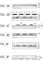
- Figs. 2A to 2F show schematically process for producing an optical recording medium substrate of the present invention.
- Fig. 3 shows an electrodeposition step
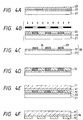
- Figs. 4A to 4F show schematically another process for producing an optical recording medium substrate of the present invention.
- Figs. 5A and 5B show schematically still another process for producing an optical recording medium substrate of the present invention.
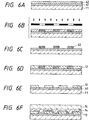
- Figs. 6A to 6F show schematically still another process for producing an optical recording medium substrate of the present invention.
- Figs. 7A and 7B explain a method of evaluation of an optical card of the present invention.
- Fig. 8 shows a method of calculation of a track-traversing signal.
- Figs. 9A and 9B show schematic sectional views of still another optical recording medium of the present invention.
- Figs. 10A to 10F show schematically still another process for producing an optical recording medium substrate of the present invention.
- Fig. 11 explains another electrodeposition step.
- Fig. 12 shows a schematic sectional view of still another optical recording medium of the present invention.
- Figs. 13A to 13E show schematically still another process for producing an optical recording medium of the present invention.
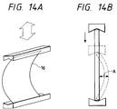
- Figs. 14A and 14B explain schematically a flection test of an optical card of the present invention.
- Figs. 15A to 15C show schematically still another process for producing an optical recording medium of the present invention.
- Fig. 16 shows a schematic sectional view of still another optical recording medium of the present invention.
- Figs. 17A and 17B show schematic sectional views of still another optical recording medium of the present invention.
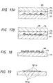
- Fig. 18 shows a schematic sectional view of an original plate for producing an optical recording medium shown in Fig. 17A.
- Fig. 19 shows a schematic sectional view of an original plate for producing an optical recording medium shown in Fig. 17B.
- Fig. 20 shows a schematic sectional view of still another optical recording medium of the present invention.
- Figs. 21A to 21C show schematically still another process for producing an optical recording medium of the present invention.
- Figs. 22A to 22D show schematically still another process for producing an optical recording medium of the present invention.
- Fig. 23 shows a schematic sectional view of still another optical recording medium of the present invention.
- Figs. 24A to 24F show schematically still another process for producing an optical recording medium of the present invention.
- Figs. 1A and 1B are schematic sectional views of an optical card of a first embodiment in a track-traversing direction.
- an electrodeposit layer 12 is provided in a pattern corresponding to preformat to form a substrate 16 for the optical recording medium.
- the area which is not covered with the electrodeposit layer 12 constitutes a tracking track 17 of the preformat.
- a recording layer 13, adhesion layer 14, and a protecting layer 15 are laminated sequentially.
- Fig. 1B is a schematic sectional view of another embodiment of the optical card of the present invention.
- An electrodeposit layer 12 is arranged selectively on the surface of a substrate material 11 to constitute the optical recording medium substrate 16, and the electrodeposit layer 12 constitutes a tracking track 17.
- the thickness of the electrodeposit layer 12 in the present invention depends of the incident direction of the light beam for recording-reproduction .
- the thickness is preferably decided to be equal substantially to the value of odd number times ⁇ /4n ED , or the value of ⁇ /8n ED (where ⁇ is the wavelength of the light beam, and n ED is the refractive index of the electrodeposit layer).
- the thickness is preferably decided to be equal substantially to the value of odd number times ⁇ /4n OP , or the value of ⁇ /8n OP (where n OP is the refractive index of the adhesion layer).
- the thickness of the electrodeposit layer is preferably ⁇ /8n ED or ⁇ /8n OP .
- the recording layer provided as above on the substrate enables generation of preformat reproduction signals with excellent contrast by utilizing an effect of interference of light.
- an optical recording medium can be obtained which is capable of giving nondeffective preformat reproduction signals with high contrast, since the thickness of the electrodeposit layer can be controlled uniformly and precisely by the quantity of electric current.
- Fig. 2 illustrates a process for producing an optical recording medium of this embodiment.
- an electroconductive layer 22 is formed on an original plate substrate 21, and further thereon a photoresist layer 23 is formed (Fig. 2A).
- the photoresist layer 23 is exposed to light in a pattern corresponding to a preformat of the optical recording medium (Fig. 2B), and is developed to uncover the electroconductive layer in accordance with the preformat pattern (Fig. 2C).
- the original plate prepared as shown in Fig. 2C is immersed into an electrodeposition solution, and electrodeposition is allowed to proceed by application of DC voltage by utilizing the electroconductive layer 22 as one electrode to form an electrodeposit layer 12 on the uncovered portion 24 of the electroconductive layer (Fig. 2D). Subsequently, a substrate material 11 is brought to close contact with the electrodeposit layer 12 on the original plate (Fig. 2E), and the electrodeposit layer is transferred onto the substrate material 11. Finally the electrodeposit layer is cured to prepare an optical recording medium substrate 16 (Fig. 2F).
- this substrate for optical recording medium having preformat pattern 17 on the surface, a recording layer, an adhesive layer, and a protecting layer is laminated to provide an optical recording medium as shown in Fig. 1.
- a pattern corresponding to a fine preformat of a micron order or a submicron order can be formed with high precision, because the electrodeposit layer is formed only on the uncovered portion of the electroconductive layer 22.
- the electrodepositable substance for forming the electrodeposit layer of the present invention may be any material which is soluble or dispersible in the electrodeposition solution and is ionizable therein, and is not specially limited. Metals and resins are useful therefor. The resins are preferred which are capable of adhering tightly to a resinous substrate material and having a refractive index close to that of the substrate material, because reflection of light at the interface between the substrate material and the electrodeposit layer is thereby suppressed.
- an electroconductive layer 22 is formed firstly on an original plate substrate 21, and then a photoresist layer 23 is formed on the electroconductive layer 22.
- Useful materials for the original plate substrate includes plastics such as polymethyl methacrylate, polycarbonate, polyethylene, polypropylene, polystyrene, polyvinyl chloride, cellulose triacetate, polyvinyl fluoride, polysulfone, polyether sulfone, polyetherimide, polymethylpentene, and the like; ceramics, and metals.
- plastics such as polymethyl methacrylate, polycarbonate, polyethylene, polypropylene, polystyrene, polyvinyl chloride, cellulose triacetate, polyvinyl fluoride, polysulfone, polyether sulfone, polyetherimide, polymethylpentene, and the like; ceramics, and metals.
- the electroconductive layer 22 to be utilized as an electrode in the electrodeposition may be made from any material which is capable of imparting electroconductivity to the surface of the original plate substrate.
- the example of the material include aluminum, copper, nickel, etc. and transparent electroconductive films such as of tin oxide and indium oxide.
- the electroconductive layer 22 can be formed by a method such as spraying, sputtering, vapor deposition, and lamination.
- the formation of the electroconductive layer may be omitted.
- a photoresist layer is formed on the electroconductive layer.
- the material useful for forming the photoresist layer includes photodecomposition type photosensitive resins containing a diazonium salt or an azide compound, photopolymerizable type photosensitive resins of cinnamoyl type, diazo type, azide type, acryloyl type, and the like; and other materials such as albumin, casein, glue, polyvinyl alcohol, and bichromate salt photosensitive solution, e.g., shellac.
- Such photoresist may be formed on the above electroconductive layer by a known coating method such as a sprinkling method, a wheeler method, a spinner ' method, an immersion method, a roller coating method, a spraying method, an electrostatic spraying method, and so forth. If the photoresist is a dry film, the photoresist layer may be formed by hot pressing. The thickness of the photoresist layer is several microns.
- the photoresist layer 23 is exposed to a pattern of light corresponding to a preformat pattern (Fig. 2B), and is developed (Fig. 2C).
- the exposure to the pattern of light corresponding to a preformat pattern is conveniently conducted by irradiation of a UV ray or an electron beam through a mask 4 such as a chrome mask used for semiconductors, a photographic film, a metal mask, a slit, and so forth. Otherwise, the exposure is conducted by irradiation of an electron beam through a metal mask, or by scanning of electron beam in a pattern without using a mask.
- a mask 4 such as a chrome mask used for semiconductors, a photographic film, a metal mask, a slit, and so forth.
- the exposure is conducted by irradiation of an electron beam through a metal mask, or by scanning of electron beam in a pattern without using a mask.
- a soluble portion formed by exposure is eliminated by use of a solvent, namely by use of a developer.
- portions of the photoresist layer are removed in a pattern to form a preformat pattern, thereby uncovered portions 25 being formed, and the original plate 26 being prepared.
- preformat in the present invention means a pattern of information formed preliminarily on an optical recording medium substrate.
- the examples therefor include tracking track in a spiral, concentric, or parallel state having a width of from 0.5 ⁇ m to 5 ⁇ m and a pitch of 1.0 ⁇ m to 15 ⁇ m for an optical disk or an optical card, and prepits such as address pits.
- the electroconductive layer is deposited at the uncovered portion by electrodeposition in an electrodeposition solution.
- the electroconductive layer is used as one electrode, and ionized and electrodepositable substance 31 migrates toward this electrode, insolubilizing and depositing on the electroconductive surface by reaction with proton formed by electrolysis of water on the electrode to form the electrodeposit layer.
- the electrodepositable material in the present invention includes conventional resins for electrodeposition coating such as those disclosed in Japanese Patent Application Laid-Open Nos. 59-114592 and 63-210901.
- resins for electrodeposition coating such as those disclosed in Japanese Patent Application Laid-Open Nos. 59-114592 and 63-210901.
- anion type electrodeposition preferred are those resins and prepolymers which have an anionic functional group like a carboxyl group originally or introduced for giving a negative charge and hydrophilicity required for deposition of the resin.
- cation type electrodeposition preferred are those resins and prepolymers which have a cationic functional group like an amino group inherently or such a group later introduced for imparting a positive charge and hydrophilicity.
- acrylic resins alkyd resins, epoxy resins, polyester resins, polyamide resins, acryl-melamine resins, prepolymers of the above polymers, curable resins cured by reaction of double bonds in the molecule like polybutadiene and ⁇ , ⁇ -ethylenic unsaturated compounds, which have the above anionic or cationic functional group.
- the above electrodepositable materials may be setting at ordinary temperature, thermosetting, or radiation-energy curing cause by UV ray or electron ray.
- the resin which is not self-curing is preferably used in combination with a melamine resin, a blocked polyisocyanate compound, or the like as a curing agent.
- the refractive index of the electrodeposit layer is desired to be less than or approximately equal to that of the substrate for receiving the electrodeposit layer in order to minimize the reflection of light at the interface between the deposition layer-receiving substrate and the electrodeposit layer.
- the refractive indexes of polycarbonate resin, polymethyl methacrylate resin and glass frequently employed as the substrate for optical recording have a refractive index respectively of 1.58, 1.48, and 1.53
- a resin employed for electrodeposition has preferably a refractive index in the range of from about 1.48 to about 1.58.
- a substrate of an optical recording medium is prepared by bringing a substrate material 11 into close contact with the original plate having an electrodeposit layer (Fig. 2E), transferring the electrodeposit layer onto the substate material, and curing the electrodeposit layer on the substrate material to obtain a polymer film arranged in pattern (Fig. 2F).
- the transfer may be conducted by use of a rubber-coated roller to press the surface of the electrodeposit layer to the surface of the substrate.
- a transfer-assisting layer 41 may be preliminarily formed on the surface of the substrate material 11 to transfer the electrodeposit layer onto the substrate material 11 by aid of the transfer-assisting layer 41 as shown in Fig. 4.
- the transfer-assisting layer 41 serves to transfer the electrodeposit layer formed on the electrode of the original plate surely onto the substrate and to retain the deposition layer on the substrate.
- the transfer-assisting layer may be an adhesion layer containing an adhesive or a sticking agent, or made of any other material which has the above-mentioned functions.
- the adhesive layer as the transfer-assisting layer includes containing a photosensitive adhesive, a heat-sensitive adhesive, a pressure-sensitive adhesive, a thermosetting adhesive, a thermoplastic adhesive, a synthetic rubber, natural rubber, gelatin, paste, or the like.
- the adhesive layer as the transfer-assisting layer may be in any form including a liquid, an emulsion, a sheet, a microcapsule, and the like.
- the liquid form of adhesives are classified into those which lose fluidity and solidify after application and those which do not solidify on use. The latter ones are called sticking agents.
- the photosensitive adhesives for the adhesive or the sticking agent for the transfer-assisting layer include UV-curable adhesives which are cured on irradiation of UV light.
- UV-curable adhesives which are cured on irradiation of UV light.
- preferred are acrylic type UV-curable adhesives, polyester type UV-curable adhesives, and epoxy type UV-curable adhesives.
- the pressure-sensitive adhesives therefor include thermoplastic rubber type hot-melt adhesives.
- Microcapsules may be used as the photosensitive, heat-sensitive, or pressure-sensitive adhesive.
- the wall of the microcapsule is made of a material which is capable of being activated by light, heat, or pressure, and the microcapsule encloses a curing agent, a crosslinking agent, a solvent, a plasticizer, or the like, whereby the capsule comes to have an adhesive function by action of light, heat, or pressure.
- thermosetting adhesive preferred are epoxy resin type adhesives which are crosslinked by heat, and phenol resins, resorcinol resins, urea resins, melamine resins and the like which are crosslinked by heat and pressure.
- thermoplastic adhesive preferred are polymers and copolymers of vinyl monomers such as vinyl acetate, acrylate esters, vinyl chloride, ethylene, acrylic acid, acrylamide, and styrene; and epoxy resins which are cured by heat and solidified by cooling.
- vinyl monomers such as vinyl acetate, acrylate esters, vinyl chloride, ethylene, acrylic acid, acrylamide, and styrene
- epoxy resins which are cured by heat and solidified by cooling.
- the transfer-assisting layer 41 on the substrate material 11 is brought into contact with the electrodeposit layer on the original plate. If the transfer-assisting layer is a photosensitive adhesive, light is projected onto the layer in this state. Then the substrate material is separated from the original plate (Fig. 4F). Thereby the electrodeposit layer is provided on the substrate material through the transfer-assisting layer 41.
- the transfer-assisting layer may be provided by coating on the substrate material. If the transfer-assisting layer is an adhesive in a sheet form, the sheet is put between the substrate material and the original plate having the electrodeposit layer to conduct transferring.
- the transfer-assisting layer is a heat-sensitive adhesive, a pressure sensitive adhesive, a heat-curable adhesive, or a thermosetting adhesive
- the original plate and the substrate material are put together with the electrodeposit layer and the transfer-assisting layer held inside, and are heated, pressed, or press-heated, and than separated.
- the transfer-assisting layer is a sticking agent
- the original plate and the substrate material put together are pressed, and then separated.
- the electrodeposit layer transferred onto the substrate material 11 in the above process is cured as mentioned above. If the electrodeposit layer is made of a photopolymerizable resin, it may separated from the substrate plate after light irradiation. The separated layer may be irradiated further to cure the layer more. If the electrodeposit layer is composed of a heat-curable resin, it may be cured either before or after the separation of the substrate. If the electrodeposit layer is composed of a pressure-curable it may be compressed with a press machine or a laminator before separation of the substrate material.
- the recording layer is formed on the transferred electrodeposit layer on the optical recording medium substrate.
- the material for the recording layer includes organic dyes such as polymethine dyes, cyanine dyes, naphthoquinone dyes, and phthalocyanine dyes; metals and semimetals as inorganic materials such as magnetooptical recording films, e.g., low-melting substances like Bi, Sn, and Te, and composite compounds having As, Se, S, O, C, etc. bonded thereto, and Te-TeO2, Tb-Fe-Co for recording according to phase difference; and silver halide for recording according to optical density change.
- organic dyes such as polymethine dyes, cyanine dyes, naphthoquinone dyes, and phthalocyanine dyes
- metals and semimetals as inorganic materials such as magnetooptical recording films, e.g., low-melting substances like Bi, Sn, and Te, and composite compounds having As, Se, S, O, C, etc. bonded thereto, and Te-TeO2, Tb-Fe-Co
- the organic dyes employed in the recording layer may be combinedly used with a stabilizer for the dyes.
- the stabilizer includes metal chelate compounds having a center atom like Zn, Cu, Ni, Cr, Co, Mo, Pd, and Zr, and polydentate ligand such as tetradentate ligands, e.g., N4, N2O2, N2S2, S4, O2S2, and O4; other tetradentate type compounds having a tridentate ligand, e.g., N2O, NO2, NS2, O3, and NOS combined with another ligand such as bidentate ligands, e.g., water, ammonia, halogen, phosphine, amine, alumine, olefin, etc.; combination of two bidentate ligands, e.g., N2, NO, O2, S2, etc.; biscyclopentadienyl ligand; cyclopentadienyltropy
- the stabilizer further includes aromatic amines and diamines, nitrogen-containing aromatic compounds and onium salts thereof such as aminium salts, diimmonium salts, pyridium salts, imidazolium salt, monolinium salts, salts of aromatic oxygen containing compounds, e.g., pyrylium salts, and the like.
- the stabilizer is suitably selected in consideration of its compatibility with the dye and the coating solvent.
- a plurality of stabilizers may be combinedly used.
- the ratio of the combination is suitably decided depending on the coating application property of the dye composition, stability of the coating film, optical properties (reflectivity and transmissivity), recording sensitivity, and so forth.
- the amount of the stabilizer to be added may be in a range of from several % to 50 % by weight based on the dye. A smaller amount of addition will not give a sufficient stabilizing effect, while excessively larger amount of addition causes reduction of the sensitivity because of the decrease of the absolute amount of the heat-mode-recording material. Therefore, the amount of addition is preferably in the range of from 10 to 30 % by weight, particularly preferably in an amount of about 20 % by weight.
- the recording layer may be prepared by a wet coating such as roll coating, wire bar coating, air knife coating, calender coating, dip coating, and spray coating, or by a dry coating such as vapor deposition, and sputtering.
- a protecting layer is laminated through an adhesion layer on the optical recording medium substrate having the recording layer depending on the practical use.
- the adhesive used for the adhesion layer in the present invention includes conventionally employed adhesives such as polymers and copolymers of vinyl acetate, acrylate esters, vinyl chloride, ethylene, acrylic acid, acrylamide or the like; thermoplastic adhesives, e.g., polyamides, polyesters, epoxy resins, etc.; adhesivies like amino resins (urea resins and melamine resins), phenol resins, epoxy resins, urethane resins, thermosetting vinyl resins; and rubber type adhesives e.g., natural rubber, nitrile rubber, chlorinated rubber, silicone rubber, etc.
- hot-melt type adhesives are applied by a dry process, and are preferable in continuous mass production. UV-curable type adhesives are also suitable in view of the improvement in mass production.
- the adhesion is conducted by lamination, hot-pressing , radiation curing, or the like method depending on the kind of the adhesive.
- the substrate material and the protecting layer may be of any material which has high light transmissivity at the side of introduction of recording and/or reproduction light.
- the material includes glass and plastics: the plastics including acrylic resins, polyester resins, polycarbonate resins, vinyl resins, polysulfone resins, polyimide resins, polyacetal resins, polyolefin resins, polyamide resins, and cellulose derivatives.
- the substrate material or the protective layer need not be light-transmissive, materials capable of protecting mechanically and chemically the recording layer are preferred, including plastics, glass, metals, ceramics, papers, and composits thereof.
- the substrate plate, the protecting layer, and the adhesion layer after adhesion are transparent to the recording/reproducing light.
- the original plate after the transfer of an electrodeposit layer 12 onto a substrate material can be used repeatedly, thus mass production of optical recording medium is feasible with high performance at low cost.
- a casting mold unit shown in Fig. 5B is prepared by use of the original plate 26 having the electrodeposit layer 12 provided through the steps shown in Figs. 2A to 2D.
- a liquid transparent resin is filled, and the resin is solidified or cured. Then the solidified or cured resin is released from the unit, thus an optical recording medium substrate being formed which has the preformat of the electrodeposit layer 12 on the simultaneously formed substrate material 11.
- the numeral 51 indicates a spacer; 52, a metal plate or a glass plate having a mirror-finished face; 53, an inlet for filling the liquid resin; and 54, a liquid resin filled in the unit.
- the resin for forming the substrate material of the optical recording medium may be any resin which is liquid before curing or polymerization.
- the examples of the resin include epoxy resins, methyl methacrylate resins, diethylene glycol resins, bisallyl carbonate resins, unsaturated polyester resins, and any other resins which are useful as a substrate of an information-recording medium.
- the substrate material is desired to be curable in the same curing method as the resin material of the electrodeposit layer.
- the electrodeposit layer is made from a thermosetting resin, a thermosetting material is used for the substrate material.
- the original plate 26 having been used can be used repeatedly, which allows the efficient production of optical recording medium substrate plate at low cost.
- a recording layer, and a protecting layer are suitably laminated to produce an optical recording medium as illustrated in Figs. 1A and 1B.
- a transparent electrode 61 which has high transmissivity to the light for recording and reproduction such as tin oxide and indium oxide (Fig. 6A).
- an insulating substance such as a photoresist 62 is applied, and is exposed to light irradiation in a pattern corresponding to the preformat pattern. The electrode is uncovered in the pattern by development (Figs. 6B and 6C).
- an electrodeposit layer 12 is deposited by electrodeposition by using the transparent electrode as one of the electrodes, and the photoresist is removed off (Figs. 6D and 6E).
- a recording layer 13, an adhesion layer 14, and a protecting layer 15 are laminated (Fig. 6F) to obtain the optical recording medium of the present invention.
- the resin for the electrodeposit layer is a cationic resin
- the transparent resin has to be used as the cathode in electrodeposition, which causes reduction reaction at the transparent electrode made of oxide, resulting damage of the transparent electrode. Therefore, the resin for the electrodeposit layer is preferably composed of an anionic resin.
- the second embodiment of the optical recording medium of the present invention is the one having a preformat pattern on a surface of a substrate and further thereon a recording layer, wherein the preformat comprises an electrodeposit layer, and the electrodeposit layer exhibits a reflectivity different from the prescribed reflectivity of the recording medium toward an information recording beam or an information reproducing beam introduced to the optical recording medium.
- Fig. 9 shows a schematic sectional view in a track-traversing direction of the optical card of the second embodiment of the present invention.
- a substrate material 91 together with a preformat 97 thereon composed of an electrodeposit layer 92 constitute an optical recording medium substrate 96.
- a recording layer 93, an adhesion layer 94, and a protecting substrate plate 95 are laminated sequentially.
- the electrodeposit layer 92 forming the preformat 97 is has a reflectivity R2 different from the reflectivity R1 of the recording layer 93 toward the information recording beam or the information reproducing beam introduced to the optical card as shown in Fig. 9B when R1 is the prescribed reflectivity of the recording layer 93 to the light beam for reproducing information and R2 is the reflectivity of the electrodeposit layer 92 which is formed preformat.
- Fig. 10 shows the process for producing the optical recording medium of the present invention.
- an electroconductive layer 102 is formed on an original plate substrate 101, and further on the electroconductive layer 102, a photoresist layer 103 is formed (Fig. 10A).
- the photoresist layer 103 is exposed to light irradiation through a mask 104 in a pattern corresponding to the preformat of the optical recording medium (Fig. 10B).
- the irradiated layer is developed to uncover the electroconductive layer in accordance with the preformat (105, Fig. 10C).
- the resulting original plate 106 is immersed in a electrodeposition solution, and electrodeposition is conducted by using the electroconductive layer 102 as one of the electrodes to deposit an electrodeposit layer 92 on the electroconductive layer (Fig.
- a recording layer, an adhesion layer, and a protecting layer are laminated on the surface of the optical recording medium substrate having a preformat 97, thus an optical recording medium as shown in Fig. 9A.
- a fine preformat is precisely formed in a micron order or a submicron order since the electrodeposit layer is formed only at the irradiated area of the electroconductive layer 102 and film thickness is controllable by quantity of the electric current in the electrodeposition.
- reflectivity of the electrodeposit layer can be adjusted by selecting suitably the material to be deposited on the electroconductive layer as the depositable substance or a co-depositable substance.
- an optical recording medium can be obtained which gives excellent track-traversing signal.
- the reflectivity R2 of the electrodeposit layer 92 and the reflectivity R1 of the recording layer 93 are considered to be substantially different if the values of R1 and R2 satisfy the relation below.
- (R1- R2) / R1 ⁇ 0.3 (if R1 ⁇ R2), or (R2 - R1) / R2 ⁇ 0.3 (if R2 ⁇ R1) preferably, (R1 - R2) / R1 ⁇ C.35 (if R1 ⁇ R2), or (R2 - R1) / R2 ⁇ 0.35 (if R2 ⁇ R1)
- track servo is conducted with high precision.
- the electrodepositing substance for forming the electrodeposit layer of this embodiment is not specially limited, but may be any substance which is soluble or dispersible in the electrodeposition solution and is ionizable in the electrodeposition solution.
- Metals and resins are useful therefor. In particular, resins are preferred because of the ease of controlling the reflectivity of the electrodeposit layer according to the kind of the recording layer.
- resins for electrodeposition paints are useful as the electrodepositing resin in the present invention.
- resins and prepolymers which have or modified to have an anionic functional group like a carboxyl group for imparting an negative charge and hydrophilicity for depositing the resin.
- resins and prepolymers which have, or modified to have, a cationic functional group like an amino group for imparting an positive charge and hydrophilicity for depositing the resin.
- the resins include those having the above-mentioned anionic functional group or a cationic group such as acrylic resins, epoxy resins, polyester resins, polyamide resins, acryl-melamine resins, and alkyd resins, and prepolymers thereof; and further include those which come to be cured by reaction of double bond in the molecule such as polybutadiene type resin and ⁇ , ⁇ -unsaturated ethylenic compounds.
- the electrodepositing resins may be cold-curable, heat-curable, radiation-curable (UV- or electron-beam-curable).
- the resins which are not self-crosslinking may be used by mixing with a melamine resin, a blocked polyisocyanate compound, or the like.
- the aforementioned resin is dispersed with a powdery substance having a high reflectivity in an electrodeposition solution.
- Electrodeposition is conducted in this dispersion to deposit the resin together with the high-reflectivity particles onto the electroconductive resin (hereinafter referred to "co-deposition") to obtain an electrodeposit layer having a high reflectivity.
- This electrodeposit layer is transferred onto a substrate material 91 to prepare an optical recording medium substrate having a preformat of high reflectivity.
- the recording layer has preferably a reflectivity of 5 to 40 %, more preferably 10 to 25 %, to the light of the wavelength of 780 to 830 nm.
- an electrodeposit layer having a low reflectivity is obtained by conducting electrodeposition in a dispersion of a low-reflectivity particles, which has high absorbance to recording- or reproducing-beam, with the above resin in an electrodeposition solution to co-deposit them on the electroconductive layer.
- This electrodeposit layer is transferred onto a substrate material 91 to prepare an optical recording medium substrate having a preformat of low reflectivity.
- the substance having a high reflectivity which can be co-deposited onto the electrodeposit layer is not limited, but may be any substance which is capable of imparting a reflectivity higher than that of the recording layer to the electrodeposit layer.
- the recording layer is made from an organic material
- highly reflective metal or alloy particles such as of Al, Cr, Ni, Ag, and Au.
- the size of the particles are to be within the range such that the particles are deposited uniformly on the electrodeposition and the precision of the preformat is not impaired.
- the average particle diameter is preferably in the range of from 0.01 to 0.5 ⁇ m.
- ultrafine metal particles which has an average particle diameter of from 0.01 to 0.1 ⁇ m obtained by hot plasma evaporation because secondary coagulation is not caused in a solution.
- the substance having a high reflectivity may be a nonmetallic powder coated at the surface by a metal (hereinafter referred to as "metallized powder").
- a metal hereinafter referred to as "metallized powder”
- Such powder may be of any material which is capable of imparting to the electrodeposit layer a reflectivity different from that of the recording layer, and is not specially limited.
- the powder includes powdery ceramic plated with a metal (metallized ceramic powder) and powdery natural mica plated with a metal (metallized natural mica), powdery resins coated with a metal, and mixtures thereof, including powdery ceramic or powdery natural mica coated at the surface with Cu, Ni, Ag, Au, Sn, or the like.
- the metallization of the surface of the powdery material is preferably conducted by use of Cu, Ag, or Ni in view of the cost, and suitably according to non-electrolytic plating.
- the powdery ceramic or the powdery natural mica preferably has an average diameter in a range of from 0.05 to 0.5 ⁇ m, more preferably from 0.2 to 0.3 ⁇ m, in consideration of the surface area contributing the surface activity, the dispersibility in a electrodeposition paint, and formation of a fine preformat with high precision.
- the ceramics in the present invention include aluminum oxide, titanium nitride, manganese nitride, tungsten nitride, tungsten carbide, lanthanum nitride, aluminum silicate, molybdenum disulfide, titanium oxide, and silicic acid.
- the natural mica includes frogovite mica, sericite mica, and muscovite mica.
- Such metallized powder which has a specific gravity lower than that of metal, improves more effectively the reflectivity than the metal powder, compared at the same content by weight.
- Surface-metallized resin powder may also be used as the metallized nonmetallic powder.
- Such powder can be prepared by forming a reflective layer of metal, e.g., copper, silver, gold, and nickel on a surface of the powder of a resin such as a fluororesin, a polyethylene resin, an acrylic resin, a polystyrene resin, a nylon resin, etc. in the same manner as in the case of ceramics.
- the resin powder also has preferably an average diameter of from about 0.05 to about 0.5 ⁇ m.
- the nonmetallic powder coated with a metal is preferred since the handling thereof is easier than the aforementioned metallic powder.
- the metallized ceramic powder and the metallized natural mica powder is advantageous in that the powder enables crosslinking of the resin by a lower energy in the process of crosslinking the resin in the electrodeposit layer.
- the electrodeposit layer having the metallized ceramic powder or the metallized natural mica powder or a mixture thereof co-deposited causes crosslinking with a lower energy.
- the surface of the powder is kept active to a certain extent by interaction between the surface of ceramic or natural mica and the plated metal, being different from the readily oxidizable metal powder, whereby the active surface serves as a crosslinking site to accelerate the crosslinking of the resin in the electrodeposit layer.
- the thickness of the metal plating on the surface of the nonmetal powder is preferably in a range of from 0.03 to 0.2 ⁇ m, preferably from 0.05 to 0.1 ⁇ m to achieve the high reflectivity of the surface and acceleration of crosslinking of the resin.
- the material having low reflectivity to be co-deposited in the electrodeposit layer may be any material which is capable of imparting to the electrodeposit layer a reflectivity lower than that of the recording medium, and is not specially limited.
- the substance may be selected from usual dyes and pigment that have a reflectivity lower than the recording layer.
- a material having a reflectivity of nearly zero such as carbon black is highly desirable.
- the recording layer has the reflectivity in a range of from 10 to 60 %, more preferably from 15 to 60 % to the light of the wavelength of 780 to 830 nm.
- the particle of low reflectivity preferably has an average particle diameter in a range of from 0.01 to 0.5 ⁇ m.
- the material having a high reflectivity or a low reflectivity is contained (amount of co-deposition) in the electrodeposit layer in such a content that the material causes substantial difference of reflectivity from the recording layer but does not impair the adherence of the electrodeposit layer to the substrate material.
- the content is preferably in a range of from 2 to 75 %, more preferably from 5 to 40 %, still more preferably from 8 to 25 % by weight in a cured electrodeposit layer.
- the content is preferably in a range of from 1 to 40 %, more preferably from 5 to 30 % by weight in consideration of the reflectivity and the properties of the coating film.
- the electroconductive particle can be identified by an X-ray microanalyzer, and the amount of co-deposition can be measured by thermogravimetry.
- Another method of controlling the reflectivity of the electrodeposit layer in this invention is to disperse light-scattering particles in the electrodeposit layer.
- the light-scattering particulate material to be co-deposited with an electrodepositing resin onto the electrode of an original plate is preferably selected from the materials which scatter and/or irregularly reflect light at the interface with the deposited resin to lower the reflectivity of the electrodeposit layer 92.
- the difference of the reflectivity from that of the electrodeposited resin is preferably not less than 0.05, more preferably not less than 0.2.
- the specific examples include glass beads, lead-containing glass beads, particulate diamond, hollow glass beads, and the like. The hollow glass beads are particularly preferred since the beads has interfaces between the resin and the particle and between the glass and air, thereby causing greater scattering and irregular reflection.
- the particulate material is suitably selected from those which give reflectivity difference from the electrodeposit resin and neither dissolve in nor react with the electrodeposited resin or paint.
- the average particle diameter of the above light-scattering particles is preferably in a range of from 0.05 to 0.5 ⁇ m, more preferably from 0.05 to 0.2 ⁇ m in order not to impair the precision of the preformat.
- the content (amount of co-deposition) of the light-scattering particles in the electrodeposit layer 92 is preferably in a range of form 5 to 50 %, more preferably from 10 to 30 %, still more preferably from 15 to 25 % by weight in the cured electrodeposit layer in consideration of adherence of the electrodeposition layer to the substrate material and flexibility of the electrodeposit layer required for flexible optical recording medium such as an optical card.
- the co-deposited particles can be identified by an X-ray microanalyzer, and the amount of the co-deposition can be measured by thermogravimetry.
- This constitution is suitably employed when the recording layer has the reflectivity in a range of from 10 to 60 %, more preferably from 15 to 40 % to the light of the wavelength of 780 to 830 nm.
- the average particle diameter of the particles incorporated in the electrodeposit layer in the present invention can be measured by a laser-diffraction/scattering type of a particle size distribution analyzer (trade name: LA-700, made by Horiba Seisakusho K.K.).
- Still another method of controlling the reflectivity of the electrodeposit layer in this embodiment is to make the electrodeposit layer porous for providing light-scattering property of the layer.
- the porosity of the electrodeposit layer can be attained by mixing to an electrodeposition paint a foaming compound which foams on light irradiation and/or heating such as zinc chloride double salts with p-diethylaminobenzenediazonium chloride, p-dimethylaminobenzenediazonium chloride, etc., azodicarbonamide, and dinitropentamethylenetetramine, then depositing it together with the electrodeposition resin onto an electrode, and then foaming the foaming compound by heating or light-irradiation of the electrodeposit layer at the time of transferring to a substrate material and/or after transferring to a substrate material.
- a foaming compound which foams on light irradiation and/or heating such as zinc chloride double salts with p-diethylaminobenzenediazonium chloride,
- the pores may be closed or opened.
- the ratio of the foamed cells, namely the void ratio is preferably in a range of from 10 to 50 %, more preferably from 15 to 35 %, still more preferably from 20 to 30 % by volume to achieve sufficient light-scattering property of the electrodeposit layer without causing embrittlement of the layer.
- This constitution is suitably employed, when the reflectivity of the recording layer is in a range of from 10 to 60 %, particularly 15 to 40 % to the light of wavelength of 780 to 830 nm.
- the original plate 106 is prepared in the same manner as in the original plate 26 employed in the optical recording medium of the aforementioned first embodiment of the present invention, so that the description thereof is omitted here.
- An original plate 106 which has been prepared as above and has an electroconductive layer uncovered in a pattern corresponding to a preformat pattern, is subjected to electrodeposition in an electrodeposition solution 113 to deposit an electrodeposit layer onto the uncovered portion of the electroconductive layer.
- the electrodeposit layer is formed by using the electroconductive layer as one electrode, applying voltage between the electrode and another electrode 112 to cause migration of the electrodeposition resin material 115 which is ionized in the electrodeposition to the electrode and to deposit the material on the electroconductive layer surface.
- a particulate material 114 having a higher reflectivity or a lower reflectivity, a light-scattering particles, or a foaming compound is added together with the electrodepositing resin into the electrodeposition solution, and then the particles is deposited with the electrodepositing resin onto the electrode, thereby the electrodeposition layer being formed which has a high reflectivity or a low reflectivity.
- the reason why the resin 115 and the particles 114 deposit simultaneously is considered as below.
- the electrodepositing resin has a functional group bonded thereto which is ionized in the electrodeposition solution.
- the resin On application of a DC voltage between the article to be coated and the counter electrode, the resin is attracted to the article to be coated and deposits thereon.
- the resin is adsorbed around the electroconductive particles in the electrodeposition solution, so that the particles also migrates to the electrode (the article to be coated) with the migration of the resin to the electrode, and deposits simultaneously with the resin to form a coating film.
- the thickness of the electrodeposit layer is preferably such that the layer has a reflectivity different from that of the recording medium when the layer has been transferred on a substrate material. Specifically the layer is formed in a thickness ranging from 0.01 ⁇ m to 10 ⁇ m.
- a substrate material 91 is made to adhere closely (Fig. 10E) to transfer the electrodeposit layer onto the substrate material. Then the electrodeposit layer is cured to prepare an optical recording medium substrate.
- the transfer is practiced by bringing the surface of the electrodeposit layer into contact with the surface of the substrate.
- the pressure may be applied by means of a rubber-coated roller.
- the electrodeposit layer 92 may be transferred onto the substrate material 91 through a transfer-assisting layer as described before, thereby the precision of the transfer of the electrodeposit layer being improved further.
- the constitution employing the transfer-assisting layer is preferred for the optical recording medium of the second embodiment having an electrodeposit layer which is liable to become brittle by incorporation of co-depositing material.
- a photopolymerizable resin as the electrodepositing material may be exposed to light irradiation before transferring onto the substrate If further curing of the electrodeposit layer is desired, the layer is exposed again to light irradiation after transferring to the substrate.
- thermosetting resin as the electrodepositing material may be cured by heat treatment before or after the transfer to the substate.
- a pressure-curing material as the electrodepositing material may be transferred to the substrate by applying pressure by means of a press machine or a laminator.
- the recording layer is formed on the transferred electrodeposit layer thus prepared on the optical recording medium substrate.
- the material for the recording medium includes organic dyes such as polymethine dyes, cyanine dyes, naphthoquinone dyes, and phthalocyanine dyes; inorganic materials of metals and semimetals such as low-melting substances of Bi, An, Te, etc. and composite compounds thereof with As, Se, S, O, C, etc.; magnetooptical recording films such as Te-TeO2 type, and Tb-Fe-Co type which conduct recording by phase transition; silver halides which conduct recording in response to optical density change; and so forth.
- organic dyes such as polymethine dyes, cyanine dyes, naphthoquinone dyes, and phthalocyanine dyes
- inorganic materials of metals and semimetals such as low-melting substances of Bi, An, Te, etc. and composite compounds thereof with As, Se, S, O, C, etc.
- magnetooptical recording films such as Te-TeO2 type, and Tb-Fe-Co type which conduct recording by
- the present invention it is prefered to select a material which is capable of forming a recording layer having reflectivity different from that of the electrodeposit layer.
- the metals and alloys of high reflectivity among the above mentioned materials for recording mediums such as Bi, Sn, Te, and Te-Fe-Co contain preferably a low-reflectivity substance in the electrodeposit layer, while organic dyes of low reflectivity such as polymethine dyes and cyanine dyes contain preferably a high-reflectivity substance in the electrodeposit layer.
- An optical recording medium is obtainable which is capable of giving sufficient track-traversing signal and giving excellent contrast of recording in the case where the electrodeposition layer is made to have high reflectivity and the recording layer is made to have low reflectivity, and further a reflecting layer 121 exhibiting reflectivity of about 60 % such as of Al and Au is formed as shown in Fig. 12.
- the recording layer has reflectivity of 10 to 60 %, in particular 10 to 40 % to light of wavelength of 780 to 830 nm, the reflectivity of the recording pit portion rises, whereby influences of dirts and scratches for recording or reproducing can be avoided.
- a casting mold unit similar to the one shown in Fig. 5B is constructed by use of an original plate having an electrodeposit layer and having been obtained through the steps of Fig. 10A to 10D; a substrate material is molded therein by casting and simultaneously the electrodeposit layer 92 is transferred to form an optical recording medium substrate in one step.
- the resulting optical recording medium substrate exhibits less birefringence and has precisely formed preformat.
- a recording layer, a reflecting layer, and a protecting substrate are formed suitably to obtain an optical recording medium as shown in Fig. 9 or Fig. 12.
- the electroconductive layer 22 itself is formed in a pattern corresponding to the preformat on the original plate substrate 21 as shown in Fig. 15A; an electrodeposit layer 12 is deposited on the electroconductive layer; a casting mold unit 151 is constructed by use of the original plate; and therewith an optical recording medium substrate and an optical recording medium are produced as shown in Fig. 15B and Fig. 15C.
- the optical recording medium substrate thus prepared has the electrodeposit layer 12 embedded in the substrate material as shown in Fig. 15B. Thereby exfoliation of the electrodeposit layer from the substrate material is prevented effectively. Therefore, this is one of the preferred constitution of the optical recording medium of the second embodiment of the present invention in which the electrodeposit layer is liable to be brittle owing to incorporation of the co-depositing substance.
- a transparent electrode 131 which exhibits large transmittance to the light beam for recording and reproducing information is formed from a material such as tin oxide and indium oxide on a substrate material 91 (Fig. 13A).
- an insulating material 132 such as a photoresist is applied.
- the insulating material is exposed to light irradiation in a pattern corresponding to a preformat, and is developed to uncover the electrode in the pattern (Fig. 13B).
- electrodeposition is conducted by employing the transparent electrode as the one of the electrodes to deposit an electrodeposit layer 92; the photoresist is removed (Figs. 13C and 13D); and on the face of the formed electrodeposit layer, a recording layer, an adhesion layer, and protecting layer are laminated (Fig. 13E) to complete an optical recording medium of the present invention.
- the transparent electrode itself may be formed in a pattern, and onto the patterned transparent electrode, the electrodeposit layer is deposited.
- the optical recording medium as shown in Fig. 16 can be prepared.
- a third embodiment of the recording medium of the present invention is described below.
- the information recording medium has an electroconductive recording layer or reflecting layer, and an electrodeposit layer is provided on the recording layer or the reflecting layer.
- Figs. 17A and 17B show schematic sectional views of the optical recording medium of the third embodiment of the present invention.
- the recording medium comprises a substrate 171, an electroconductive recording layer or reflecting layer 172, an electrodeposit layer 173, an adhesion layer 174, and a protecting substrate 175.
- the optical recording medium of Fig. 17A may be prepared by forming a resist pattern 181 corresponding to a preformat on the surface of the electroconductive recording layer (or reflecting layer) 172 on the substrate 171 as shown in Fig. 18; immersing this substrate in an electrodeposition paint; conducting electrodeposition with the electroconductive recording layer (or reflecting layer) 171 employed as the one of the electrodes; washing the substrate having the electrodeposit layer with water; curing the electrodeposit layer; lifting off the resist layer; and overlaying a protecting substrate on the above-mentioned substrate at the side of the electrodeposit layer.
- the optical recording medium of Fig. 17B may be prepared by patterning an electroconductive recording layer (or reflecting layer) into a recording region 191(a) and a preformat region 191(b); immersing the substrate in an electrodeposition paint; conducting electrodeposition with the preformat region 191(b) of the electroconductive recording layer employed as the one of the electrodes; washing the substrate having the electrodeposit layer with water; curing the electrodeposit layer; and overlaying a protecting substrate on the above-mentioned substrate at the side of the electrodeposit layer.
- the electroconductive recording layer or the electroconductive reflecting layer in the present invention has preferably electroconductivity sufficient for deposition of the electrodeposition resin on application of electric current for electrodeposition.
- the electroconductive layer comprises an electroconductive material capable of recording, such material including metals, metal oxides, carbon, and electroconductive polymers: specifically metals such as Au, Cu, Al, and Te, metal oxides such as TeO, carbon such as carbon black, and electroconductive polymers such as polyacetylene, polypyrrole, polythiophene, and polyaniline.
- electroconductive material capable of recording, such material including metals, metal oxides, carbon, and electroconductive polymers: specifically metals such as Au, Cu, Al, and Te, metal oxides such as TeO, carbon such as carbon black, and electroconductive polymers such as polyacetylene, polypyrrole, polythiophene, and polyaniline.
- the electroconductive layer when employed as the reflecting layer, it comprises a reflective material having electroconductivity: such material including metals, metal oxides, and electroconductive polymers: specifically metals such as Au, Cu, Ni, and Al, and electroconductive polymers such as polyacetylene, polypyrrole, and polyphenylene.
- the electrodeposit layer in the present invention, is desired to have reflectivity different much more from that of the recording layer (or reflecting layer).
- the reflectivity of the electrodeposit layer can be controlled by incorporating a particulate material having high reflectivity, a particulate material having low reflectivity, or light-scattering particles into the electrodeposit layer, or otherwise making the electrodeposit layer porous.
- the electrodeposit layer when the electroconductive recording layer or the electroconductive reflecting layer has reflectivity in a range of from 10 to 60 %, in particular, from 20 to 60 % to light of the wavelength of from 780 to 830 nm, the electrodeposit layer has preferably lower reflectivity.
- a fourth embodiment of the optical recording medium of the present invention is described below.
- a recording layer composed of an electrodeposit layer is arranged in a pattern corresponding a preformat on a substrate.
- Fig. 20 shows a schematic sectional view of an optical recording medium of this embodiment.
- the medium comprises a substrate 201, a recording layer 202 composed of an electrodeposit layer arranged in a pattern corresponding to a preformat on the substrate, an adhesion layer 203, and a protecting substrate 204.
- the optical recording medium of this embodiment can be prepared according to any of the above-described method in which a preformat is formed of an electrodeposit layer on the aforementioned substrate.
- the recording layer composed of the electrodeposit layer in this embodiment may be formed by conducting electrodeposition by use of an electrodeposition paint containing a particulate material to constitute the recording material.
- the particulate material to constitute the recording material includes organic dyes such as polymethine dyes, cyanine dyes, naphthoquinone dyes, anthraquinone derivatives, chromanium compounds, azo compounds, phthalocyanine pigments, and carbon black; inorganic materials of metals and semimetals such as low-melting substances of Bi, Sn, Te, etc. and composite compounds thereof with As, Se, S, O, C, etc.; Te-TeO2 type substances which conduct recording by phase transition; and silver halides which conduct recording in response to optical density change; and so forth.
- phthalocyanines are preferred, since they exhibit relatively high reflectivity and have sufficient dispersibility in the electrodeposition paint.
- the recording material is contained in the recording layer composed of the electrodeposit layer at a content in a range of from 5 to 50 %, more preferably from 10 to 40 %, still more preferably from 20 to 35 % by weight in consideration of the recording sensitivity of the recording layer (electrodeposit layer), the film properties of the electrodeposit film such as flexibility and adhesiveness.
- the content of the recording material in the electrodeposit layer can be measured by thermogravimetry when the recording material is electroconductive, and by light transmittance when the recording medium contains an organic dye or pigment.
- an optical recording medium is produced, as shown in Figs. 21A, 21B, and 21C, by arranging an electrode layer 212 in a pattern on an original plate substrate 211, depositing an electrodeposit layer 202 for a recording layer, constructing a casting mold unit 216 by use of the original plate 213, filling a liquid resin 214 into the unit, curing the resin, and releasing the mold, thus transferring the electrodeposit layer 202 onto the substrate 214.
- this method high recording sensitivity can be obtained without retarding the information recording even when a protecting layer 215 is provided on the substrate, since vacant spaces are formed on the recording layer.
- a fifth embodiment of an optical recording medium of the present invention has a preformat layer composed of an electrodeposit layer and a recording layer composed of an electrodeposit layer formed respectively on a substrate.
- Figs. 22A and 22B illustrate schematically a process for producing an optical recording medium of the fifth embodiment.
- an electroconductive layer 222 e.g., a transparent electrode composed of In2O3 or the like
- an electroconductive pattern 222a for electrodepositing a recording layer and another electroconductive pattern 222b for electrodepositing a preformat layer are formed by use of photolithography.
- the substrate 221 is immersed in an electrodeposition paint for preformat layer formation, and a preformat layer 223 is deposited by employing the electroconductive pattern 222b as the one of the electrodes.
- the substrate 221 is immersed in another electrodeposition paint for recording layer formation, and a recording layer 224 is deposited by employing the electroconductive pattern 222a as the one of the electrodes. Thereafter the preformat layer and the recording layer is cured. If necessary, a protecting substrate 225 is provided with interposition of a spacer as shown in Fig. 22C, or with interposition of an adhesion layer 226 as shown in Fig. 22D. Thereby a recording medium having both a preformat layer composed of an electrodeposit layer and a recording layer composed of an electrodeposit layer is prepared. In preparing the optical recording medium, the reflectivity of the preformat layer and that of the recordeing layer are preferably controlled so as to make larger the reflectivity difference. The methods for controlling the reflectivity of the electrodeposit layer is already described above.
- an optical recording medium may be prepared by providing an original plate having a preformat layer composed of an electrodeposit layer and a recording layer formed on an original plate substrate in the same manner as described by reference to Figs. 22A and 22B, bringing the original plate into direct contact with a substrate material or into indirect contact with it by interposition of a transfer-assisting layer, and transferring the electrodeposition layer onto the substrate material.
- an optical recording medium having an electrodeposit layer 223, 224 embedded in a substrate 231 as shown in Fig. 23 may be prepared by constructing a casting mold unit by use of the above-mentioned original plate having a preformat layer composed of an electrodeposit layer and a recording layer composed of an electrodeposit layer as shown in Fig. 21, and filling a liquid resin into this mold, solidifying or curing the resin.
- an optical recording medium may be prepared as below.
- an electroconductive layer 242 is formed on an original plate substrate 241.
- a resist pattern 243 is formed corresponding to a preformat (Fig. 24A).
- the original plate is immersed in an electrodeposition paint for preformat layer formation, and electrodeposition is conducted by employing the electroconductive layer 242 as the one of the electrodes to deposit a preformat layer 244.
- the layer is washed with water and is cured (Fig. 24B).
- the original plate, after the resist pattern is lifted off (Fig. 24C) is immersed in an electrodeposition paint, and electrodeposition is conducted by employing the electroconductive layer 242 as the one of the electrode to deposit a recording layer 245.
- the preformat layer has been cured to become insulating, so that the recording layer does not deposit on the preformat layer (Fig. 24D).
- a substrate material 246 is brought into close contact with the preformat layer 244 and the recording layer 245 with or without interposition of a transfer-assisting layer, and the preformat layer 244 and the recording layer 245 are transferred onto the substrate material.
- a protecting substrate is provided on the preformat layer 244 and the recording layer 245 with interposition of an adhesion layer to bond closely or to form air gaps on the recording layer 245.
- a casting mold unit is constructed by use of the original plate of Fig. 24C, thereby the formation of the substrate material and the transfer of the preformat layer 244 and the electrodeposit layer 245 are conducted in one step.
- the preformat layer has preferably reflectivity substantially higher than that of the recording layer.
- the preformat layer preferably contains a powdery metal or a powdery metallized material.
- the preformat layer has preferably reflectivity substantially lower than that of the recording layer.
- the preformat layer preferably contains a light-scattering particulate material or carbon black, or the electrodeposit layer is made porous.
- the wording of "substantially higher (or lower) reflectivity" is defined already.
- an optical recording medium capable of giving preformat reproducing signal with high contrast is provided according to the present invention by employing, for patterning, an electrodeposition layer which can be controlled in layer thickness and/or reflectivity by applied quantity of electric current or the kind and amount of an additive.
- optical recording medium having a preformat of high precision can be prepared with extreme ease.
- the original plate can be used repeatedly, so that the mass productivity of the recording medium is greatly improved.
- the intensity of reflected light is detected by oscilloscope while the laser spot 71 traverses the tracking track 17 (Fig. 7).
- the contrast is obtained from the detected wave form of the reflected light (a track-traversing signal: fig. 8).
- Va represents output voltage when the laser spot is at the intermediate position between two tracking tracks 17
- Vb represents the output voltage when the laser spot is on the tracking track 17.
- Contrast ratio (Va - Vb)/(Va) Wavelength of laser beam: 830 nm Power of laser beam: 0.5 mW (Optical disks)/ 0.27 mW (Optical cards) Spot diameter (on recording face): 1.6 ⁇ m (Optical disks)/ 3 ⁇ m (Optical cards) Incident direction of laser beam: Substrate side
- the electroconductive powdery material dispersed in the electrodeposit layer was determined by a thermogravimetric analyzer (trade name: Thermal Analysis System 7 Series, made by Perkin-Elmer Co.), and the organic dye or pigment in the electrodeposit layer was determined by measuring light transmittance.
- An optical disk of 350 mm in diameter having a preformat constituted of an electrodeposit layer was prepared according to the procedure below.
- a glass plate (size: 400 mm x 400 mm, thickness: 5 mm) mirror-finished at one face was employed as the original plate substrate. Copper was vacuum-deposited on the mirror face side of the glass plate to form an electroconductive layer of 0.5 mm thick.
- a photoresist (trade name: WAYCOAT HPR204, made by Fuji Hanto Electronics Technology Co.) was applied on the surface of the electroconductive layer to give a dry thickness of 700 ⁇ by means of a roll coater, and was pre-baked at 100°C for 20 minutes.
- the photoresist layer was subjected to pattern exposure by UV ray irradiation through a photomask attached tightly to the photoresist layer.
- the photomask had a pattern corresponding to concentric tracking tracks of 0.6 ⁇ m in width and 1.6 ⁇ m in pitch formed as a preformat by means of an electron beam writing apparatus.
- the photoresist on the exposed area was dissolved off by immersing a developer solution (LSI developer solution, made by Fuji Hanto Electronics Technology Co.). Then post-baking was conducted at 100°C for 20 minutes. Thus an original plate 26 was prepared.
- LSI developer solution made by Fuji Hanto Electronics Technology Co.
- a cationic electrodeposition solution was prepared as below.
- An organic polymer was prepared as a binder by copolymerization of N,N-diethylaminoethyl methacrylate, styrene, ethyl acrylate, and a compound derived by equimolar reaction of p-hydroxybenzoic acid with glycidyl acrylate.
- the organic polymer was constituted of the above monomer in molar ratio of 3:2:4:1, and had a weight-average molecular weight of 70,000.
- a cationic photosensitive resin composition 80 parts by weight of the above organic polymer binder, 0.5 part by weight of 2,2-dimethoxy-2-phenylacetophenone, and 14.5 parts by weight of trimethylolpropane triacrylate were mixed to prepare a cationic photosensitive resin composition.
- This composition was diluted with ethylene glycol monobutyl ether to have a volatile matter content of 80 %, and neutralized with 0.5 equivalent of acetic acid, and further diluted with deionized water to a concentration of 15 % by weight to obtain an electrodeposition solution.
- the original plate 26 was immersed into this electrodeposition solution. By employing the electroconductive layer as the cathode and the metal vessel of the bath as the positive electrode, DC voltage of 5 - 10 V was applied for one minute. The original plate was taken out, washed with water sufficiently, and dried to obtain an electrodeposit layer 12.
- the surface of the electrodeposit layer 12 formed in a pattern on the original plate 26 was brought into contact with a polycarbonate resin substrate material of 350 mm diameter and 1.2 mm thick, and the electrodeposit layer was transferred onto the substrate material by means of a rubber-coated roller.
- the transferred electrodeposit layer was exposed to light entirely from the top by means of a high pressure mercuric lamp at an intensity of 200 mJ/cm2 to cure the electrodeposit layer 12.
- the resulting preformat pattern layer had a thickness of 700 ⁇ .
- a tellurium oxide recording layer 21 was formed to a thickness of 300 ⁇ by sputtering.
- a protecting substrate 15 made of a polycarbonate resin (diameter: 350 mm, inside diameter: 28 mm, thickness: 1.2 mm) was sticked with interposition of an adhesion layer 14 of ethylenevinyl acetate copolymer type to prepare an optical disk.
- optical disk tester trade name:OMS-2000, made by Nakamichi Co.
- the optical disk was rotated at 600 rpm, and the optical head was fixed (by cutting the track servo) at positions of the radiuses of 150 mm (r150), 70 mm (r70), and 30 mm (r30).
- the track-traversing signals were measured at each position. As the results, little variation was observed as shown in Table 1. Therefore, the optical disk was found to give tracking signals with uniformity and high contrast.
- An optical disk as shown in Fig. 1B was formed in the same manner as in Example 1, in which the tracking tracks were formed by the region having no electrodeposit layer 12.
- Example 2 An optical disk similar to that of Example 2 was prepared in a similar manner as in Example 2.
- the electrodeposition solution used was an acryl-melamine resin (trade name: Hani Bright C-IL, made by Hani Kasei K.K.) diluted to a solid concentration of 15 % by weight.
- an electrodeposit layer was deposited in a thickness of 800 ⁇ on an original plate at a bath temperature of 25°C and pH 8 - 9 by employing the electroconductive layer of the original plate as the anode and a stainless steel plate as the counter electrode and by applying voltage of 5 - 10 V for one minute.
- the electrodeposition layer was transferred onto an optical disk substrate material made of polycarbonate of 350 mm in diameter, 28 mm in inside diameter, and 1.2 mm in thickness, and cured by heating in an oven kept at 96°C for about 120 minutes to obtain an optical disk in which electrodeposit-lacking regions are the tracking tracks.
- a 3 wt% solution of the polymethine dye shown below in diacetone alcohol was applied by spin coating to form a recording layer of 1000 ⁇ thick.
- an UV-curable adhesive containing plastic beads (0.5 mm in diameter) is applied on the inner periphery portion and the outer periphery portion in a width of 1 mm.
- a protecting substrate (350 mm in diameter, 28 mm in inside diameter, 1.2 mm in thickness) made of a polycarbonate resin was laminated, and the outer and inner periphery portions were irradiated with UV light.
- an optical disk was completed.
- An optical disk substrate was prepared by injection molding: the disk substrate being in a size of 350 mm in outside diameter, 28 mm in inside diameter, and 1.2 mm in thickness and having track grooves of 0.6 ⁇ m in width, 1.6 ⁇ m in pitch and 800 ⁇ in depth on the surface.
- a recording layer and a protecting layer were formed in the same manner as in Example 1 to complete an optical disk.
- This optical disk was measured for the track-traversing signals at the positions of r150, r70, and r30 in the same manner as in Example 1.
- the average values of the track-traversing contrast at r150, r70, and r30 are shown in Table 1.
- a polycarbonate disk mirror-finished on the both faces in a size of 350 mm in outside diameter, 28 mm in inside diameter, and 1.2 mm in thickness was prepared by injection molding.
- a 2P layer was formed from the photo-curable resin composition having the components below, and by a 2P forming process.
- An optical disk substrate was prepared which has spiral track grooves of 0.6 ⁇ m in width, 1.6 ⁇ m in pitch, and 800 ⁇ in depth.
- This optical disk substrate was dried at 120°C for 3 hours to remove any residual monomer and to complete the polymerization.
- the recording layer and the protecting layer were laminated in the same manner as in Example 3 to complete an optical disk.
- An original plate substrate was prepared by vacuum depositing copper on a mirror-finished face of glass plate (size: 100 mm x 100 mm, thickness: 5 mm) having been mirror-finished at one face to form an electroconductive layer of 0.5 mm thick on the plate.
- a photoresist (trade name: WAYCOAT HPR204, made by Fuji Hanto Electronics Technology Co.) was applied on the surface of the electroconductive layer to give a dry thickness of 1300 ⁇ by means of a roll coater, and was pre-baked at 100°C for 20 minutes to form a photosensitive layer.
- the photoresist layer was subjected to pattern exposure by UV ray irradiation through a photomask attached tightly to the photosensitive layer.
- the photomask had a pattern corresponding to a preformat pattern for a linear tracking track pattern of 3 ⁇ m in width and 12 ⁇ m in pitch for an optical card, the pattern being written by an electron beam writing apparatus.
- the photoresist on the exposed area was dissolved off by immersion in a developer solution (LSI developer solution, made by Fuji Hanto Electronics Technology Co.). Then post-baking was conducted at 100°C for 20 minutes. Thus an original plate was prepared.
- LSI developer solution made by Fuji Hanto Electronics Technology Co.
- electrodeposit layer 12 was deposited on the original plate in an electrodeposition solution which was a 15 wt% solution of an acryl-melamine resin (trade name: Hani Bright C-IL, made by Hani Kasei K.K.) at a bath temperature of 25°C and pH 8 - 9 by employing the electroconductive layer of the original plate as the anode and a stainless steel plate as the counter electrode and by applying voltage of 15 - 20 V for one minute.
- an electrodeposition solution which was a 15 wt% solution of an acryl-melamine resin (trade name: Hani Bright C-IL, made by Hani Kasei K.K.) at a bath temperature of 25°C and pH 8 - 9 by employing the electroconductive layer of the original plate as the anode and a stainless steel plate as the counter electrode and by applying voltage of 15 - 20 V for one minute.
- the electrodeposition layer was transferred onto an optical card substrate material made of polymethyl methacrylate of 54 mm wide, 85 mm long, and 0.4 mm thick.
- an optical card substrate was obtained in which the tracking tracks are formed by regions where the electrodeposit layer of about 1380 ⁇ thick was not formed. It was observed by optical microscopy (x2000) that the electrodeposit layer was transferred precisely onto the substrate material.
- Example 3 On this substrate, a solution of the polymethine dye used in Example 3 at a concentration of 3 % by weight in diacetone alcohol was applied by spin coating to form a recording layer of 1000 ⁇ thick.
- a hot-melt adhesive film of ethylene-vinyl acetate copolymer type, and a protecting substrate made of polymethyl methacrylate in a size of 54 mm in width, 85 mm in length, and 0.3 mm in thickness were laminated and heat pressed through hot rolls at a surface temperature of 110°C to complete an optical card.
- a optical card substrate was prepared by transferring stripe-shaped track grooves of 3 ⁇ m in width and 12 ⁇ m in pitch by a compression method onto a surface of a substrate material made of polymethyl methacrylate in a size of 54 mm in length, 85 mm in width, and 0.4 mm in thickness.
- an optical card was prepared in the same manner as in Example 4, and track-traversing signals were observed in the same manner as in Example 4. As the results, the signals were observed to fluctuate.
- the values of contrast of the track-traversing signals are shown in Table 2.
- optical card substrate prepared in the same manner as in Example 4 was evaluated in adhesion between the electrodeposit layer and the substrate material by flection test as below.
- the short sides of the optical card substrate was held as shown in Fig. 14A.
- the card was flexed as shown in Fig. 14B where the degree of flection of the middle portion of the card as indicated by the symbol A is 20 mm. This flection was repeated 250 times. Thereafter the long sides of the card substrate was held in the same manner and the card was flexed 250 times to cause the flexion A of 10 mm.
- the state of the electrodeposit layer at the surface of the optical card was examined by optical microscopy. No peeling of the electrodeposit layer was observed.
- An original plate having an electrodeposit layer was prepared in the same manner as in Example 1.
- An optical disk substrate was prepared by applying on the surface of a glass disk of 350 mm in diameter, 28 mm in inside diameter, and 1.2 mm in thickness a UV-curable resin (trade name UVX-SS120, made by Three Bond K.K.) by spin coating in a thickness of 2 to 4 ⁇ m as a transfer-assisting layer, placing the above original plate on the substrate material to bring the electrodeposit layer into contact with the uncured transfer-assisting layer, and curing both the transfer-assisting layer and the electrodeposit layer by light irradiation from the glass substrate material side by means of a high-pressure mercury lamp (120 W/cm) at an irradiation intensity of 500 mJ/cm2, and then separating the original plate and the substrate material.
- a UV-curable resin trade name UVX-SS120, made by Three Bond K.K.
- the thickness of the electrodeposit layer transferred onto the substrate material was 700 ⁇ .
- the electrodeposit layer 12 was found to be precisely transferred from the original plate 26.
- Tellurium oxide recording layer 21 was formed by sputtering in a thickness of 300 ⁇ . Thereon, a protecting glass substrate 15 (350 mm in diameter, 28 mm in inside diameter, 1.2 mm in thickness) was bonded to complete an optical disk through an adhesive layer 14 made of ethylene-vinyl acetate copolymer.
- the resulting optical disk was evaluated in the same manner as in Example 1. The results are shown in Table 3-(1).
- An original plate having an electrodeposit layer was prepared in the same manner as in Example 4.
- An optical card substrate was prepared by applying on the surface of an optical card substrate made of polycarbonate of 54 mm in width, 85 mm in length, and 0.4 mm in thickness a UV-curable resin (trade name UVX-SS120, made by Three Bond K.K.) by spin coating in a thickness of 2 to 4 ⁇ m as a transfer-assisting layer, placing the above original plate on the substrate material to bring the electrodeposit layer into contact with the uncured transfer-assisting layer, curing both the transfer-assisting layer and the electrodeposit layer by light irradiation from the glass substrate material side by means of a high-pressure mercury lamp (120 W/cm) at an irradiation intensity of 500 mJ/cm2 and additional heating in an oven at 96°C for about 120 minutes, and then separating the original plate and the substrate material.
- a high-pressure mercury lamp 120 W/cm
- additional heating in an oven at 96°C for about 120 minutes
- a hot-melt adhesive film of ethylene-vinyl acetate copolymer type, and a protecting substrate made of polymethyl methacrylate in a size of 54 mm in width, 85 mm in length, and 0.3 mm in thickness were laminated and heat pressed through hot rolls at a surface temperature of 110°C to complete an optical card.
- the resulting optical card was evaluated in the same manner as in Example 4. The results are shown in Table 3-(2).
- optical card substrate prepared in the same manner as in Example 6 was evaluated for adhesion between the electrodeposit layer and the substrate material by flection test as below.
- the short sides of the optical card substrate was held as shown in Fig. 14A.
- the card was flexed as shown in Fig. 14B where the degree of flexion of the middle portion of the card as indicated by the symbol A is 25 mm. This flection was repeated 300 times. Thereafter the long sides of the card substrate was held in the same manner and the card was flexed 300 times to cause the flexion A of 15 mm.
- the state of the electrodeposit layer at the surface of the optical card was observed by optical microscopy. No peeling of the electrodeposit layer was observed.
- An optical card original plate 106 was prepared in the same manner as in Example 4 except that the dry thickness of the photoresist layer was 0.1 ⁇ m.
- a cationic electrodeposition solution was prepared as below.
- An organic polymer was prepared as a binder by copolymerization of N,N-diethylaminoethyl methacrylate, styrene, ethyl acrylate, and a compound derived by equimolar reaction of p-hydroxybenzoic acid with glycidyl acrylate.
- the resulting organic polymer was constituted of the above monomer in molar ratio of 3:2:4:1, and had a weight-average molecular weight of 70,000.
- a cationic photosensitive resin composition 80 parts by weight of the above organic polymer binder, 0.5 part by weight of 2,2-dimethoxy-2-phenylacetophenone, and 14.5 parts by weight of trimethylolpropane triacrylate were mixed to prepare a cationic photosensitive resin composition.
- This composition was diluted with ethylene glycol monobutyl ether to have a volatile matter content of 80 %, and neutralized with 0.5 equivalent of acetic acid, and further diluted with deionized water to a solid concentration of 10 % by weight.
- the electrodeposition resin composition prepared as above To the 100 part by weight of the electrodeposition resin composition prepared as above, 25 parts by weight of powdery nickel having an average particle diameter of 0.1 ⁇ m was added, and the powdery nickel was dispersed by means of a ball mill for 30 hours. Then the dispersion was diluted with deionized water to a concentration of 1.5 % by weight to obtain an electrodeposition solution. The original plate 106 was immersed in this electrodeposition solution, and DC voltage of 30 V was applied for one minute by employing the electroconductive layer 102 as the cathode and the metallic bath vessel as the anode. The original plate was taken out, washed sufficiently with water, and dried, thus electrodeposit layer 92 being obtained in a thickness of 2 ⁇ m.
- the surface of the electrodeposit layer 92 formed in a pattern on the original plate 106 was brought into contact with an acrylic resin substrate material 91 in a size of 100 mm x 100 mm and 0.4 mm thick, and the electrodeposit layer 92 was transferred onto the polymethylmethacrylate substrate material by means of a rubber-coated roller.
- substrate material was wholely exposed to light irradiation with a high-pressure mercury lamp from above at an intensity of 200 mJ/cm2 (exposed face) to cure the electrodeposit layer 12.
- the amount of deposition of nickel in the electrodeposit layer was 25 % by weight.
- an acrylic resin substrate of 0.3 mm thick was bonded by use of a hot-melt type ethylene-vinyl acetate adhesive.
- the resulting article was cut by laser to prepare an optical card of 54 mm in width, 86 mm in length and 0.76 mm in thickness.
- the amount of the deposited carbon black in the electrodeposit layer was 20 % by weight.
- An optical card was prepared in the same manner as in Example 7 except that 15 parts by weight of carbon black having an average particle diameter of 0.05 - 0.1 ⁇ m was used in place of the powdery nickel in the electrodeposit layer.
- a preformat pattern was formed on an acrylic substrate in the same manner as in Example 8.
- a thin Te-Cu-Pb metal film was vapor-deposited in a thickness of 300 ⁇ by sputtering by use of a sputtering target of Te-Cu-Pb alloy at an Ar gas pressure of 5 x 10 ⁇ 2 torr with an applied voltage of 400 V for 90 seconds to form a recording layer 93.
- An original plate for an optical card was prepared in the same manner as in Example 4, in which dry thickness of the photoresist was 2 ⁇ m.
- alumina having an average particle diameter of 0.3 ⁇ m coated with electroless-plating nickel in a thickness of 0.1 ⁇ m was dispersed in 100 parts by weight of a curing-agent-containing acryl-melamine resin (trade name: Hani Bright C-IL, made by Hani Kasei K.K.) by means of a ball mill for 30 hours.
- the dispersion was diluted with a deionized water to a concentration of 15 % by weight for use for electrodeposition solution.
- an electrodeposition layer 12 containing alumina was deposited on the original plate by employing the electroconductive layer of the original plate as the anode and a stainless steel plate as the counter electrode at a bath temperature of 25°C at pH 8-9 by application of voltage of 30 V for one minute.
- the original plate having the electrodeposit layer was brought into contact with a transparent polycarbonate substrate material of 0.4 mm thick.
- the electrodeposit layer was transferred onto the polycarbonate substrate material by use of a rubber-coated roller.
- the electrodeposit layer transferred onto the polycarbonate substrate material was cured in an oven at 97°C for 60 minutes to prepare an optical card substrate having a preformat pattern composed of the electrodeposit layer of 2 ⁇ m thick.
- the amount of the deposited nickel in the electrodeposition layer was 15 % by weight.
- the cyanine dye represented by the formula below: was applied in a thickness of 1000 ⁇ as the recording layer on the preformat-pattern face, and further thereon a polycarbonate substrate of 0.3 mm thick was bonded as the protecting layer through a vinyl acetate type hot-melt adhesive. This article was punched out to obtain an optical card of 54 mm in width and 86 mm in length.
- An original plate for an optical card was prepared in the same manner as in Example 4.
- an electrodeposit layer containing the powdery nylon plated with silver was deposited on the original plate by employing the electroconductive layer of the original plate as the anode and a stainless steel plate of 0.5 mm thick as the counter electrode at a bath temperature of 25°C at pH 8-9 by application of voltage of 30 V for one minute.
- the amount of the deposited powdery nylon plated with silver in the electrodeposition layer was 25 % by weight.
- the original plate having the electrodeposit layer was brought into contact with an amorphous polyolefin substrate material of 0.4 mm thick.
- the electrodeposit layer was transferred onto the substrate material by use of a rubber-coated roller.
- the electrodeposit layer transferred onto the substrate material was cured in an oven at 100°C for 120 minutes to prepare an optical card substrate having a preformat pattern composed of the electrodeposit layer of 2 ⁇ m thick.
- TeO was vapor deposited in a thickness of 300 ⁇ as the recording layer, and further thereon an amorphous polyolefin substrate of 0.3 mm thick was bonded as the protecting layer through an epoxy adhesive.
- This article was cut in a size of 54 mm in width and 85 mm in length to prepare an optical card.
- An optical substrate for an optical card having a preformat constituted of an electrodeposit layer was prepared according to the procedure below.
- a polymethyl methacrylate resin plate (100 mm long, 100 mm wide, 0.4 mm thick) was employed as the original plate substrate.
- a transparent electrode 102 of indium oxide was formed by sputtering.
- a photoresist (trade name: WAYCOAT HPR204, made by Fuji Hanto Electronics Technology Co.) was applied on the surface of the indium oxide film to give a dry thickness of 0.1 ⁇ m by means of a roll coater, and was pre-baked at 100°C for 20 minutes to form a photoresist layer 103.
- the photoresist layer was subjected to pattern exposure by UV ray irradiation through a photomask attached tightly to the photoresist layer.
- the photomask 104 had a linear pattern of 3 ⁇ m in width and 12 ⁇ m in pitch corresponding to preformat pattern for tracking track for an optical card in pitch by means of an electron beam writing apparatus.
- the photoresist on the exposed area was dissolved off by immersing a developer solution (LSI developer solution, made by Fuji Hanto Electronics Technology Co.). Then the uncovered indium oxide film was removed by etching, and remaining photoresist was removed by a remover. Thus an original plate 26 having a transparent electrode in a pattern was prepared.
- LSI developer solution made by Fuji Hanto Electronics Technology Co.
- an original plate which has an electrodeposit layer 92 containing carbon black in a pattern.
- a transparent polycarbonate substrate material 91 of 0.4 mm thick was laminated with interposition of an ethylene-ethyl acrylate copolymer hot-melt sheet as the transfer-assisting layer onto the above original plate having the electrodeposit layer.
- the laminated matter was passed through a laminator at a roller temperature of 130°C, and then the substrate material 91 was separated from the original plate 106.
- the substrate having the transferred electrodeposit layer was heated in an oven at 97°C for 60 minuted to cure the transferred layer to obtain an optical card substrate having a preformat pattern constituted of the electrodeposit layer of 2 ⁇ m thick.
- the content of the carbon black in the electrodeposit layer was 25 % by weight.
- the face of the optical card substrate having the preformat was observed by optical microscopy, and it was found that the electrodeposit layer was transferred with high precision from the original plate to the substrate material.
- the cyanine dye represented by the formula below: was applied as the recording layer on the preformat-pattern face, and further thereon a polymethyl methacrylate substrate of 54 mm wide, 85 mm long, and 0.3 mm thick as the protecting substrate and an ethylene-ethyl acrylate copolymer type hot-melt adhesive were laminated.
- This article was hot-pressed through a hot roll having a surface temperature of 110°C to obtain an optical card.
- An original plate substrate was prepared by vacuum-depositing copper on a mirror-finished face of glass plate of 5 mm thick having been mirror-finished at one face to form an electroconductive layer of 0.5 mm thick on the plate.
- a photoresist (trade name: WAYCOAT HPR204, made by Fuji Hanto Electronics Technology Co.) was applied on the surface of the electroconductive layer to give a dry thickness of 0.5 ⁇ m by means of a roll coater, and was pre-baked at 100°C for 20 minutes to form a photosensitive layer.
- the photoresist layer was subjected to pattern exposure by UV ray irradiation through a photomask attached tightly to the photosensitive layer.
- the photomask had a pattern corresponding to a preformat pattern for a spiral tracking track pattern of 0.6 ⁇ m in width and 1.6 ⁇ m in pitch for an optical disk, the pattern having being written by an electron beam writing apparatus.
- the photoresist on the exposed area was dissolved off by immersion in a developer solution (LSI developer solution, made by Fuji Hanto Electronics Technology Co.). Then, post-baking was conducted at 100°C for 20 minutes. Thus an original plate was prepared.
- LSI developer solution made by Fuji Hanto Electronics Technology Co.
- a cationic electrodeposition solution was prepared as below.
- a organic polymer was prepared as a binder by copolymerization of N,N-diethylaminoethyl methacrylate, styrene, ethyl acrylate, and a compound derived by equimolar reaction of p-hydroxybenzoic acid with glycidyl acrylate.
- the resulting organic polymer was constituted of the above monomer in molar ratio of 3:2:4:1, and had a weight-average molecular weight of 70,000.
- a cationic photosensitive resin composition 80 parts by weight of the above organic polymer binder, 0.5 part by weight of 2,2-dimethoxy-2-phenylacetophenone, and 14.5 parts by weight of trimethylolpropane triacrylate were mixed to prepare a cationic photosensitive resin composition.
- This composition was diluted with ethylene glycol monobutyl ether to have a volatile matter content of 80 %, and neutralized with 0.5 equivalent of acetic acid, and further diluted with deionized water to a solid concentration of 10 % by weight.
- a transparent substrate material of polymethyl methacrylate of 5 inches in diameter and 1.2 mm in thickness was brought into close contact, and the electrodeposit layer was transferred to a substrate material. Then the original plate was separated.
- the substrate material was exposed to UV irradiation with a high pressure mercury lamp at an intensity of 200 mJ/cm2 to cure the electrodeposit layer on the substrate material.
- a substrate for an optical disk was obtained which had a preformat pattern constructed of an electrodeposit layer of 1 ⁇ m thick.
- the content of the gold-plated powdery mica was 15 %by weight.
- the anthraquinone derivative shown by the formula below: was formed in a thickness of 1200 ⁇ , and further thereon a substrate made of polymethyl methacrylate was bonded with interposition of a spacer of 0.3 mm thick by use of a silicone type adhesive to complete an optical disk.
- An InO2 thin film was formed in a thickness of 350 ⁇ by sputtering on a methyl methacrylate resin substrate of 350 mm in diameter and 1.2 mm in thickness.
- a photoresist (trade name: WAYCOAT HPR204, made by Fuji Hanto Electronics Technology K.K.) was applied in a thickness of 2 ⁇ m by a spinner, and the applied photoresist was pre-baked at 100 °C for 20 minutes.
- the photoresist layer was scanned with UV ray in a pattern corresponding to a preformat pattern, and was developed to prepare an original plate having a resist pattern of an uncovered transparent electrode in spiral of 0.6 ⁇ m in width and 1.6 ⁇ m in pitch.
- an electrodeposition solution was prepared by dispersing 25 parts by weight of powdery Ag having an average particle diameter of 0.2 ⁇ m in 100 parts by weight of an acryl-melamine resin (trade name Hani Bright C-IL, made by Hani Kasei K.K.) by means of a ball mill for 30 hours, and diluting the dispersion with deionized water to a solid content of 15 % by weight.
- an acryl-melamine resin trade name Hani Bright C-IL, made by Hani Kasei K.K.
- the original plate was immersed in this electrodeposition solution, and an electrodeposit layer 12 was deposited by conducting electrodeposition by employing the transparent electrode as the anode and a stainless steel plate as the counter electrode.
- the electrodeposit layer was washed with water, and cured by heat treatment in an oven at 130°C for 60 minutes.
- the thickness of the electrodeposition layer forming the preformat pattern was about 3000 ⁇ .
- the Ag content in the electrodeposit layer was 25 % by weight.
- the reflectivity of the electrodeposit layer was about 60-70 %.
- phthalocyanine was vapor-deposited as a recording layer in a thickness of 1000 ⁇ . Thus an optical disk was completed.
- An optical disk was prepared in the same manner as in Example 14 except that 20 % by weight of carbon black having an average particle diameter of 0.07 ⁇ m was dispersed in place of the powdery Ag in the electrodeposition solution, and TeO was vapor-deposited as the recording layer in a thickness of 400 ⁇ .
- the content of carbon black in the electrodeposit layer was 25 % by weight.
- An optical disk of 350 mm in diameter having a preformat constituted of an electrodeposit layer was prepared according to the procedure below.
- a glass plate (size: 400 mm x 400 mm, thickness: 5 mm) mirror-finished at one face was employed as the original plate substrate. Copper was vacuum-deposited on the mirror-face side of the glass plate to form an electroconductive layer of 0.5 mm thick.
- a photoresist (trade name: WAYCOAT HPR204, made by Fuji Hanto Electronics Technology Co.) was applied on the surface of the electroconductive layer to give a dry thickness of 700 ⁇ by means of a roll coater, and was pre-baked at 100°C for 20 minutes.
- the photoresist layer was subjected to pattern exposure by UV ray irradiation through a photomask attached tightly to the photoresist layer.
- the photomask had a pattern corresponding to concentric tracking tracks of 0.6 ⁇ m in width and 1.6 ⁇ m in pitch formed as a preformat by means of an electron beam writing apparatus.
- the photoresist on the exposed area was dissolved off by immersing a developer solution (LSI developer solution, made by Fuji Hanto Electronics Technology Co.). Then post-baking was conducted at 100°C for 20 minutes. Thus an original plate 106 was prepared.
- LSI developer solution made by Fuji Hanto Electronics Technology Co.
- a cationic electrodeposition solution was prepared as below.
- a organic polymer was prepared as a binder by copolymerization of N,N-diethylaminoethyl methacrylate, styrene, ethyl acrylate, and a compound derived by equimolar reaction of p-hydroxybenzoic acid with glycidyl acrylate.
- the organic polymer was constituted of the above monomer in molar ratio of 3:2:4:1, and had a weight-average molecular weight of 70,000.
- a cationic photosensitive resin composition 80 parts by weight of the above organic polymer binder, 0.5 part by weight of 2,2-dimethoxy-2-phenylacetophenone, and 14.5 parts by weight of trimethylolpropane triacrylate were mixed to prepare a cationic photosensitive resin composition.
- This composition was diluted with ethylene glycol monobutyl ether to have a volatile matter content of 80 %, and neutralized with 0.5 equivalent of acetic acid, and further diluted with deionized water to a volatile matter content of 90 %.
- the electrodeposition resin composition prepared as above 10 parts by weight of powdery alumina having average particle diameter of 0.3 ⁇ m plated with electroless-plated gold in a thickness of 0.1 ⁇ m was dispersed by means of a ball mill for 30 minutes. The dispersion was diluted with deionized water to a solid concentration of 15 % by weight for use for electrodeposition solution. The original plate was immersed into this electrodeposition solution. An electrodeposit layer containing the powdery alumina plated with gold was deposited in a pattern on the original plate by employing the electroconductive layer of the original plate as the cathode and a 0.5mm-thick stainless steel plate as the counter electrode by application of voltage of 30 V for one minute. Thus an original plate was prepared which has an electrodeposit layer that contains gold-plated powdery alumina in a pattern.
- a UV-curable resin (trade name UVX-SS120, made by Three Bond K.K.) was applied by spin coating in a thickness of 2-4 ⁇ m as the transfer-assisting layer.
- the substrate material was superposed on the original plate with the resins uncured such that the electrodeposit layer was brought into contact with the transfer-assisting layer.
- the transfer-assisting layer and the electrodeposit layer were both cured by irradiation of light with a metal halide lamp at 120 W/cm at an intensity of 500 mJ/cm2 from the glass substrate side.
- the substrate material was separated from the original plate, thus completing an optical disk substrate.
- the thickness of the electrodeposit layer on the substrate material was 1 ⁇ m.
- the optical disk substrate was observed with an optical microscope,and found that the electrodeposit layer 12 was transferred precisely onto the original plate 26.
- the content of powdery alumina plated with gold in the electrodeposit layer was 18 % by weight.
- a recording layer was formed by applying a 3 wt% solution of a polymethine dye (trade name: IR-820, made by Nippon Kayaku Co., Ltd.) in diacetone alcohol in a thickness of 1000 ⁇ .
- a protecting substrate made of glass of 350 mm in diameter, 28 mm in inside diameter, and 1.2 mm in thickness was bonded with interposition of a spacer of 0.3 mm thick through a silicone type adhesive to complete an optical disk.
- An optical card was prepared in the same manner as in Example 7 except that, after formation of the recording layer from IR820 in Example 7, Al was vapor-deposited thereon in a thickness of 200 ⁇ .
- An optical disk was prepared in the same manner as in Example 13 except that, after formation of the anthraquinone film as the recording layer in Example 13, Au was vapor-deposited thereon in a thickness of 150 ⁇ .
- the reflectivities of the recording layers and the preformat pattern portions (electrodeposit layers) of the optical cards and optical disks were measured by condensing and projecting laser light of wavelength of 830 nm onto the layers from the substrate side at a beam diameter of 3 ⁇ m for the cards and 0.5 ⁇ m for the disks.
- the positions of the light projection were nine spots randomly selected on the face of the cards and the disks.
- the average values of the reflectivities are shown in the Table below provided that the reflectivity of total reflection mirror is 100 %.
- An optical card substrate was prepared in the same manner as in Example 12 except that the amount of the deposition of carbon black in the electrodeposit layer was 70 % by weight.
- An optical card substrate was prepared in the same manner as in Example 19 except that the amount of the deposition of carbon black in the electrodeposit layer was 85 % by weight.
- optical card substrates of Example 19 and Reference Example 1 were subjected to flection test as below.
- the short sides of the optical card substrate was held as shown in Fig. 14A.
- the card was flexed as shown in Fig. 14B where the degree of flexion of the middle portion of the card as indicated by the symbol A is 15 mm. This flection was repeated 200 times. Thereafter the long sides of the card substrate was held in the same manner and the card was flexed 200 times to cause the flexion A of 5 mm.
- the state of the electrodeposit layer at the surface of the optical card was observed by optical microscopy. As the result, no peeling of the electrodeposit layer was observed with the optical card substrate of Example 19, while some cracks were observed at the surface of the electrodeposit layer of the optical card of Reference Example 1.
- An optical card was prepared in the same manner as in Reference Example 1 except that the transfer-assisting layer was not provided. As the result of the flection test as in Reference Example 1, a part of the electrodeposit layer was found to have come off.
- An optical card original plate was prepared in the same manner as in Example 4 except that the dry thickness of the photoresist was 5 ⁇ m.
- a cationic photosensitive electrodeposition resin composition was prepared as below.
- An organic polymer was prepared as a binder by copolymerization of N,N-diethylaminoethyl methacrylate, styrene, ethyl acrylate, and a compound derived by equimolar reaction of p-hydroxybenzoic acid with glycidyl acrylate.
- the organic polymer was constituted of the above monomer in molar ratio of 3:2:4:1, and had a weight-average molecular weight of 70,000.
- a cationic photosensitive resin composition 80 parts by weight of the above organic polymer binder, 0.5 part by weight of 2,2-dimethoxy-2-phenylacetophenone, and 14.5 parts by weight of trimethylolpropane triacrylate were mixed to prepare a cationic photosensitive resin composition.
- This composition was diluted with ethylene glycol monobutyl ether to have a volatile matter content of 80 %, and neutralized with 0.5 equivalent of acetic acid, and further diluted with pure water to a volatile matter content of 90 %.
- the aforementioned original plate was immersed in the cationic electrodeposition paint containing the glass beads, and voltage of 30 V was applied for one minute between the electroconductive layer as the cathode and the metallic bath vessel as the anode. Then the original plate was taken out and washed sufficiently with water. The resin adhering to the electrode having been used for application of voltage became insoluble and was not washed off by water. After washing with water, the original plate was dried to obtain an electrodeposit layer.
- a substrate made of polymethyl methacrylate of 100 mm wide, 100 mm length, and 0.4 mm thickness was laminated, and brought in close contact with the electrodeposit layer by means of a rubber-coated roll.
- the electrodeposit layer was entirely irradiated from above with a high-pressure mercury lamp at an intensity of 200 mJ/cm2 to cure the electrodeposit layer.
- a high-pressure mercury lamp at an intensity of 200 mJ/cm2 to cure the electrodeposit layer.
- the resulting electrodeposit layer had a thickness of 0.1 ⁇ m, and contained glass beads at a content of 25 % by weight.
- a 3.0 wt% solution of an organic dye IR820 (made by Nippon Kayaku Co., Ltd) in diacetone alcohol was applied by spin-coating to prepare a recording layer having a dry thickness of 100 5 nm.
- an acrylic resin substrate of 0.3 mm thick was bonded by use of a hot-melt type ethylene-vinyl acetate adhesive.
- the resulting article was cut by laser to complete an optical card of 54 mm in width, 86 mm in length and 0.76 mm in thickness.
- An original plate for an optical card was prepared in the same manner as in Example 20.
- a cationic photosensitive electrodeposition resin composition was prepared as below.
- An organic polymer was prepared as a binder by copolymerization of N,N-diethylaminoethyl methacrylate, styrene, ethyl acrylate, and a compound derived by equimolar reaction of p-hydroxybenzoic acid with glycidyl acrylate.
- the organic polymer was constituted of the above monomer in molar ratio of 3:2:4:1, and had a weight-average molecular weight of 70,000.
- a cationic photosensitive resin composition 80 parts by weight of the above organic polymer binder, 0.5 part by weight of 2,2-dimethoxy-2-phenylacetophenone, and 14.5 parts by weight of trimethylolpropane triacrylate were mixed to prepare a cationic photosensitive resin composition.
- This composition was diluted with ethylene glycol monobutyl ether to have a volatile matter content of 80 %, and neutralized with 0.5 equivalent of acetic acid, and further diluted with pure water to a volatile matter content of 90 %.
- the aforementioned original plate was immersed in the cationic electrodeposition paint containing the glass beads, and voltage of 30 V was applied for one minute between the electroconductive layer as the cathode and the metallic bath vessel as the anode. Then the original plate was taken out and washed sufficiently with water. After washing, the original plate was dried to obtain an electrodeposit layer.
- the content of the glass beads in the electrodeposit layer is 25 % by weight.
- the original plate having the electrodeposit layer and a transparent substrate material made of polymethyl methacrylate of 0.4 mm thick having the electrodeposit layer were put together with the electrodeposit layer inside and with a sheet of ethylene-ethyl acrylate copolymer held therebetween.
- the combined sheets were bonded by means of a laminator at a roller temperature of 130°C.
- the substrate material was then separated from the original plate, whereby the electrodeposit layer was transferred onto the transparent substrate material of polymethyl methacrylate.
- the transferred electrodeposit layer was cured by heating in an oven at 90°C for 60 minutes, thereby an optical card substrate being obtained.
- a layer of the cyanine dye represented by the structural formula below was provided as the recording layer:
- a polymethyl methacrylate plate of 0.3 mm thick was bonded with interposition of a hot-melt adhesive composed of an ethylene-ethyl acrylate copolymer.
- the resulting article was punched in a size of a card of 54 mm wide and 86 mm long. Thus an optical card was completed.
- An original plate for an optical card was prepared in the same manner as in Example 20.
- a cationic photosensitive electrodeposition resin composition was prepared as below.
- An organic polymer was prepared as a binder by copolymerization of N,N-diethylaminoethyl methacrylate, styrene, ethyl acrylate, and a compound derived by equimolar reaction of p-hydroxybenzoic acid with glycidyl acrylate.
- the organic polymer was constituted of the above monomer in molar ratio of 3:2:4:1, and had a weight-average molecular weight of 70,000.
- 80 parts by weight of the above organic polymer binder, 0.5 part by weight of 2,2-dimethoxy-2-phenylacetophenone, and 14.5 parts by weight of trimethylolpropane triacrylate were mixed to prepare a cationic photosensitive resin composition.
- This composition was diluted with ethylene glycol monobutyl ether to have a volatile matter content of 80 % by weight, and neutralized with 0.5 equivalent of acetic acid, and further diluted with pure water to a volatile matter content of
- the aforementioned original plate was immersed in the cationic electrodeposition paint, and voltage of 30 V was applied for one minute between the electroconductive layer as the cathode and the metallic bath vessel as the anode. Then the original plate was taken out and washed sufficiently with water. After washing, the original plate was dried to obtain an electrodeposit layer thereon.
- a casting mold unit as shown in Fig. 5B was constructed. Therein a liquid epoxy resin of the blending composition below was filled, and cured at 100°C for 10 hours to cure the epoxy resin and the electrodeposit layer.
- the glass bead content in the electrodeposit layer was 25 % by weight.
- the epoxy resin formed integrally with the electrodeposit layer was removed from the casting mold. Then the projection of the resin corresponding to the inlet of the resin was cut off by means of a sander. Thus an optical card substrate was obtained which is made of a transparent epoxy resin composition having a transferred electrodeposit layer of preformat.
- the substrate exhibited only a little birefringency caused by molding strain since it was formed by cast molding.
- the phase difference in the substrate of 100 x 100 mm was 0.1 - 5 nm (double paths).
- An original plate for an optical card was prepared in the same manner as in Example 20.
- An electrodeposition resin composition was prepared by mixing 100 parts by weight of a curing-agent-containing acryl-melamine resin (trade name Hani Bright C-IL, made by Hani Kasei K.K.) and 20 parts by weight of an aqueous 10% solution of azodicarbonamide as a blowing agent. With this composition, electrodeposition was conducted by applying voltage of 30 V for one minute between the patterned original plate as the anode and a 0.5 mm-thick stainless steel plate as the counter electrode at a bath temperature of 25°C and pH 8-9. The electrodeposit layer formed had a thickness of 2.5 ⁇ m.
- a curing-agent-containing acryl-melamine resin trade name Hani Bright C-IL, made by Hani Kasei K.K.
- a patterned original plate By washing with water after the electrodeposition, a patterned original plate was provided which had a preformat pattern composed of an electrodeposit layer containing a foaming ink.
- a casting mold unit was constructed as shown in Fig. 5B. In this mold unit, the liquid epoxy resin having the blending composition below was filled, and was cured at 100°C for 10 hours.
- the cast-molded matter was removed from the casting mold.
- the projection of the resin corresponding to the inlet of the resin was cut off by means of a sander.
- an optical card substrate was obtained which is made of a transparent epoxy resin composition having a transferred electrodeposit layer of preformat.
- the electrodeposit layer slightly foamed owing to the heat of cast molding.
- the deposit layer was further allowed to foam by heating in an oven at 150°C for 60 minutes.
- an optical card substrate was provided which had an electrodeposit layer of void ratio of 30 %.
- the substrate exhibited only a little birefringency caused by molding strain since it was formed by cast molding.
- the phase difference in the substrate of 100 x 100 mm was 0.1 - 5 nm (double path).
- An original plate for an optical card was prepared in the same manner as in Example 20.
- An electrodeposition resin composition was prepared by mixing 100 parts by weight of a curing-agent-containing acryl-melamine resin (trade name Hani Bright C-IL, made by Hani Kasei K.K.) and 20 parts by weight of an aqueous 10% solution of azodicarbonamide as a blowing agent. With this composition, electrodeposition was conducted by applying voltage of 30 V for one minute between the patterned original plate as the anode and a 0.5 mm-thick stainless steel plate as the counter electrode at a bath temperature of 25°C and pH 8-9. The electrodeposit layer formed had a thickness of 2.5 ⁇ m. By washing with water after the electrodeposition, an original plate was provided which had a preformat composed of an electrodeposit layer containing a foaming ink.
- a curing-agent-containing acryl-melamine resin trade name Hani Bright C-IL, made by Hani Kasei K.K.
- a 0.4mm-thick transparent polycarbonate substrate material was brought into contact with the original plate having the electrodeposit layer, and the electrodeposit layer was transferred onto the polycarbonate substrate material by means of a rubber-coated roller.
- the substrate having the transferred electrodeposit layer was heated in an oven at 150°C for 60 minutes to allow the electrodeposit layer to foam.
- an optical card substate was completed which had an electrodeposit layer having a void ratio of 30%.
- a layer of the cyanine dye represented by the structural formula below was provided as a recording layer in a thickness of 1000 ⁇ :
- a polycarbonate substrate of 0.3 mm thick was bonded with interposition of a hot-melt adhesive of a vinyl acetate copolymer type.
- the resulting article was punched in a size of a card of 54 mm wide and 86 mm long. Thus an optical card was completed.
- An In2O3 thin film was formed in a thickness of 500 ⁇ by sputtering on a methyl methacrylate resin substrate of 0.4 mm thick, 10 cm long, and 6 cm wide.
- a photoresist (trade name: WAYCOAT HPR204, made by Fuji Hanto Electronics Technology K.K.) was applied in a thickness of 2 ⁇ m by a spinner, and the applied photoresist was pre-baked at 100 °C for 20 minutes. The photoresist layer was then exposed to UV light in a preformat pattern, and developed to form a resist pattern in stripe of 12 ⁇ m in pitch and 3 ⁇ m in width.
- the In2O3 layer was etched by argon plasma to form a pattern of the transparent electrode.
- An electrodeposition paint was prepared by mixing and dispersing 80 % by weight of an anionic acryl-melamine resin (trade name: Hani Bright C-IL, made by Hani Kasei K.K.) and 20 % by weight of phthalocyanine having particle diameters of 0.1 to 0.3 ⁇ m and diluting the resulting dispersion with deionized water to a solid content of 15 % by weight.
- the above patterned transparent electrode substrate was immersed into this electrodeposition paint. Electrodeposition was conducted by employing the transparent electrode as the anode. The substrate having the electrodeposit was washed with water and heat-treated at 97°C for 60 minutes for curing to form an electrodeposit layer of 3 ⁇ m wide.
- TeO layer was formed as a recording layer in a thickness of 300 ⁇ by sputtering. Thereon a 0.3mm-thick methyl methacrylate resin plate as a protecting substrate was bonded with an adhesive. The resulting article was cut in a size of 86 mm long and 54 mm wide to complete an optical card.
- the phthalocyanine content in the electrodeposit layer was 25 % by weight.
- optical cards of Examples 20 to 25 were subjected to measurement of reflectivities of the recording layers and of the preformat pattern portion (electrodeposit layer) at randomly selected nine spots for each card by projecting laser light of wavelength of 830 nm condensed to a beam diameter of 3 ⁇ m. As shown in Table 6, sufficient difference of the reflectivity was observed between the recording layer and the electrodeposit layer.
- optical cards of Examples 20 to 25 were subjected to measurement of the track-transversing signal in the same manner as in Example 4.
- the maximum values, the minimum values, and the average values of the track-traversing signal were shown in Table 7. As shown in the table, uniform track signals were obtained.
- optical cards of Examples 20 to 25 were subjected to measurement of flection test in the same manner as in Example 4.
- the occurrence of peeling of the electrodeposit layer from the substrate was examined with an optical microscope (magnification: 2000x). The results are shown in Table 7.
- An optical card was prepared in the same manner as example 23 except that the void ratio of the electrodeposition layer was controlled to be 45 %.
- An optical card was prepared in the same manner as example 23 except that the void ratio of the electrodeposition layer was controlled to be 60 %.
- optical card substrates of Example 24 and Reference Example 3 were subjected to flection test as below.
- the short sides of the optical card substrate was held as shown in Fig. 14A.
- the card was flexed as shown in Fig. 14B where the degree of flexion of the middle portion of the card as indicated by the symbol A is 15 mm. This flection was repeated 150 times. Thereafter the long sides of the card substrate was held in the same manner and the card was flexed 150 times to cause the flexion A of 5 mm.
- the state of the electrodeposit layer at the surface of the optical card was examined by optical microscopy. As the result, no peeling of the electrodeposit layer was observed in the optical card substrate of Example 24, while a part of the electrodeposit layer came off in the optical card of Reference Example 3.
- a transparent electrode of indium oxide was formed by sputtering on a methyl methacrylate resin substrate of 0.4 mm thick.
- a resist mask was formed according to a photolithography technique.
- the InO2 was etched directly to pattern the transparent electrode into an optical disk preformat corresponding to a spiral tracking track of 0.6 ⁇ m in width and 1.6 ⁇ m in pitch. This was used as an original plate.
- An electrodeposition paint was prepared by mixing and dispersing 80 % by weight of an anionic acryl-melamine resin (trade name: Hani Bright C-IL, made by Hani Kasei K.K.) and 20 % by weight of particulate diamond having an average particle diameter of 0.2 ⁇ m and diluting the resulting dispersion with deionized water to a solid content of 15 % by weight.
- the original plate was immersed into this electrodeposition paint. Electrodeposition was conducted by employing the electrode of the original plate as the anode.
- the substrate having the electrodeposit was washed with water and heat-treated at 97°C for 60 minutes for curing to form an electrodeposit layer of 0.3 ⁇ m.
- a glass disk substrate which had been optically polished on both faces and washed was superposed on this electrodeposit layer, and the electrodeposit layer was transferred onto the glass substrate by rubber coated roller to complete an optical disk substrate.
- the electrodeposit layer contained the diamond at a content of 25 % by weight.
- phthalocyanine was vapor-deposited as a recording layer, thereby an optical disk being completed having a recording layer having refectivity of 14 - 16 %.
- An optical disk original plate was prepared in the same manner as in Example 1.
- An electrodeposition resin composition was prepared by mixing 100 parts by weight of a curing-agent-containing acryl-melamine resin (trade name Hani Bright C-IL, made by Hani Kasei K.K.) and 20 parts by weight of an aqueous 10% solution of N,N′-dinitrosopentamethylenetetramine as a blowing agent. With this composition, electrodeposition was conducted by applying voltage of 30 V for one minute between the patterned original plate as the anode and a 0.5 mm-thick stainless steel plate as the counter electrode at a bath temperature of 25°C and pH 8-9. The electrodeposit layer formed was 2.5 ⁇ m. By washing with water after the electrodeposition, an original plate was provided which had a preformat composed of an electrodeposit layer containing a foaming ink.
- a curing-agent-containing acryl-melamine resin trade name Hani Bright C-IL, made by Hani Kasei K.K.
- a UV-curable resin (trade name UVX-SS120, made by Three Bond K.K.) was applied on a glass substrate in a shape of a disk of 5 inches in diameter and 1.2 mm in thickness. This resin-coated substrate was put together so as to have the electrodeposit layer and the adhesive layer inside. This superposed article was heated at 150°C for 60 minutes to cure and bond the adhesive layer and the electrodeposit layer. Then the electrodeposit layer was separated and transferred from the original plate glass substrate to complete an optical disk provided with an electrodeposit layer having a void ratio of 30 %.
- a layer of the anthraquinone derivative represented by the structural formula below: was provided as a recording layer in a thickness of 1100 ⁇ so as to show the reflectivity of 20 % to light of wavelength of from 780 to 830 nm.
- a glass substrate of 1.2 mm thick was bonded with interposition of a spacer of 0.3 mm thick with a silicone type adhesive to complete an optical disk.
- the contrast of track-traversing signals of the optical disks of Examples 27 and 28 was measured in the same manner as in Example 1. As shown in Table 8, the disks exhibited uniform track-traversing signals with high contrast.
- a transparent electrode of InO2 (indium oxide) was formed in a thickness of 350 ⁇ by sputtering on a glass substrate of 0.5 mm thick, 10 cm long, and 6 cm wide.
- an optical card original plate which has, on a glass substrate, an InO2 pattern in stripes of 3 ⁇ m wide and 12 ⁇ m pitch.
- An electrodeposition paint was prepared by mixing and dispersing 100 parts by weight of an acrylmelamine resin (trade name: Hani Bright C-IL, made by Hani Kasei K.K.) and 10 parts by weight of alumina of an average particle diameter of 0.3 ⁇ m and covered with nonelectroplated nickel of 0.1 ⁇ m thick, and diluting the resulting dispersion with deionized water to a solid content of 5 % by weight.
- electrodeposition was conducted by employing the InO2 layer of the original plate as the anode and a stainless plate as the counter electrode at a bath temperature of 25°C and pH of 8-9 by application of voltage of 30 V for one minute.
- an original plate was prepared which has electrodeposit layer in a pattern containing nickel-plated alumina.
- a casting mold cell as shown in Fig. 15 was constructed. Therein a epoxy resin of the blending composition below was filled, and cured at 100°C for 10 hours.
- an optical card substrate which comprises a transparent epoxy resin composition and a transferred recording layer.
- the substrate exhibited only a little birefringency caused by molding strain since it was formed by cast molding.
- the phase difference in the substrate was 0.1 - 5 nm (double paths).
- the electrodeposit layer contained the nickel-plated alumina at a content of 10 % by weight.
- the resulting optical card substrate was subjected to a flection test.
- the short sides of the optical card substrate was held as shown in Fig. 14A.
- the card was flexed as shown in Fig. 14B where the degree of flection of the middle portion of the card as indicated by the symbol A is 25 mm. This flection was repeated 500 times. Thereafter the long sides of the card substrate was held in the same manner and the card was flexed 500 times to cause the flection A of 15 mm.
- the state of the electrodeposition at the surface of the optical card was observed by optical microscopy. No peeling of the electrodeposit layer was observed.
- An electroconductive Te layer was formed as a recording layer in a thickness of 300 ⁇ on a methyl methacrylate resin substrate of 0.3 mm thick, 10 cm long, and 6 cm wide.
- a photoresist (trade name: WAYCOAT HPR204, made by Fuji Hanto Electronics Technology K.K.) was applied in a thickness of 2 ⁇ m by a spinner, and the applied photoresist was pre-baked at 100 °C for 20 minutes. The photoresist layer was then exposed to UV light in a preformat pattern, and developed to form a resist pattern in stripes of 12 ⁇ m in pitch and 9 ⁇ m in width.
- a preformat pattern layer constituted of the electrodeposit layer was formed by conducting electrodeposition by employing as the electrode the electroconductive layer having the resist pattern insulating layer.
- An electrodeposition paint was prepared by mixing and dispersing 80 % by weight of an anionic acryl-melamine resin (trade name: Hani Bright C-IL, made by Hani Kasei K.K.) and 20 % by weight of phthalocyanine having particle diameter of 0.1 to 0.3 ⁇ m and diluting the resulting dispersion with deionized water to a solid content of 15 % by weight.
- the above patterned TeO-coated substrate was immersed into this electrodeposition paint. Electrodeposition was conducted by employing the TeO layer as the anode.
- the substrate having the electrodeposit was washed with water and heat-treated at 97°C for 60 minutes for curing to form an electrodeposit layer of 3 ⁇ m wide.
- the content of the phthalocyanine in the electrodeposit layer was 25 % by weight.
- the resulting substrate having a patterned preformat pattern layer was bonded by an adhesive to a transparent substrate composed of methyl methacrylate resin of 0.4 mm thick, and was cut into an optical card size, thus an optical card being completed.
- a cationic electrodeposition resin composition was prepared as below.
- An organic polymer was prepared as a binder by copolymerization of N,N-diethylaminoethyl methacrylate, styrene, ethyl acrylate, and a compound derived by equimolar reaction of p-hydroxybenzoic acid with glycidyl acrylate.
- the organic polymer was constituted of the above monomer in molar ratio of 3:2:4:1, and had a weight-average molecular weight of 70,000.
- a cationic photosensitive resin composition 80 parts by weight of the above organic polymer binder, 0.5 part by weight of 2,2-dimethoxy-2-phenylacetophenone, and 14.5 parts by weight of trimethylolpropane triacrylate were mixed to prepare a cationic photosensitive resin composition.
- This composition was diluted with ethylene glycol monobutyl ether to have a volatile matter content of 80 % by weight, and neutralized with 0.5 equivalent of acetic acid, and further diluted with pure water to a volatile matter content of 90 % by weight.
- an electrodeposition solution To 80 % by weight of the electrodeposition resin composition prepared as above, 20 % by weight of carbon black having particle diameters of 0.5 to 1 ⁇ m was dispersed to prepare an electrodeposition solution.
- the substrate having the patterned electroconductive layer prepared above was immersed in the electrodeposition solution, and voltage of 30 V was applied for one minute by employing the Al of the electroconductive layer as the cathode to form an electrodeposit layer. Then the original plate was taken out and washed sufficiently with water. The resin was cured by irradiation with a high-pressure mercury lamp (200 mJ/cm2) to prepare on optical card substrate having an electrodeposit layer of 3.0 ⁇ m thick.
- the electrodeposit layer contained the carbon black at a content of 30 % by weight.
- the resulting substrate having a patterned preformat pattern layer was bonded by an hot-melt adhesive sheet of an ethylene-vinyl acetate copolymer to a transparent substrate composed of methyl methacrylate resin of 0.4 mm thick, and was cut into an optical card size. Thus an optical card being completed.
- Al was vapor-deposited in a thickness of 300 ⁇ as an electroconductive layer on a glass plate of 0.5 mm thick, 10 cm long, and 6 cm wide.
- a photoresist (trade name:WAYCOAT HPR204, made by Fuji Hanto Electronics Technology K.K.) was applied in a thickness of 2 ⁇ m by a spinner, and the applied photoresist was pre-baked at 100 °C for 20 minutes. The photoresist layer was then exposed to UV light in a preformat pattern, and developed to form a resist pattern in stripes of 12 ⁇ m in pitch and 9 ⁇ m in width.
- SiO2 was sputtered in a thickness of 200 ⁇ . and then the resist was lifted off, thereby an original plate having an insulating SiO2 layer formed on the electroconductive Al layer.
- a cationic photosensitive resin composition was prepared as below.
- An organic polymer was prepared by copolymerization of N,N-diethylaminoethyl methacrylate, styrene, ethyl acrylate, and a compound derived by equimolar reaction of p-hydroxybenzoic acid with glycidyl acrylate.
- the organic polymer was constituted of the above monomer in molar ratio of 3:2:4:1, and had a weight-average molecular weight of 70,000.
- a cationic photosensitive resin composition 80 parts by weight of the above organic polymer binder, 0.5 part by weight of 2,2-dimethoxy-2-phenylacetophenone, and 14.5 parts by weight of trimethylolpropane triacrylate were mixed to prepare a cationic photosensitive resin composition.
- This composition was diluted with ethylene glycol monobutyl ether to have a volatile matter content of 80 % by weight, and neutralized with 0.5 equivalent of acetic acid, and further diluted with pure water to a volatile matter content of 90 % by weight.
- the substrate having the patterned electroconductive layer prepared above was immersed in the electrodeposition paint, and DC voltage of 30 V was applied for one minute by employing the Al of the electroconductive layer as the cathode to form an electrodeposit layer. Then the original plate was taken out and washed sufficiently with water. Thus an original plate for an optical card was provided.
- the original plate having the electrodeposit layer was bonded to a transparent substrate made of polymethyl methacrylate of 0.4 mm thick with the electrodeposit layer held inside by an ethylene-ethyl acrylate copolymer sheet by means of a laminator at a roller temperature of 130°C.
- the substrate was separated from the original plate to transfer the electrodeposit layer to the transparent polymethyl methacrylate substrate.
- the substrate having the transferred electrodeposit layer was treated for curing with a high-pressure mercury lamp (200 mJ/cm2). Further thereon, a substrate made of polymethyl methacrylate of 0.3 mm thick was bonded as a protecting layer by use of a hot-melt adhesive composed of an ethylene-ethyl acrylate copolymer.
- the resulting article was punched out in a card size of 54 mm wide and 86 mm long.
- an optical card was completed which has a recording layer (phthalocyanine layer) of 9 ⁇ m wide arranged thereon. The content of the phthalocyanine in the recording layer of the optical card was 35 % by weight.
- An original plate having an electrodeposit layer was prepared in the same manner as in Example 32. With this original plate, a casting mold unit as shown in Fig. 5B was constructed.
- a liquid resin having the blending composition shown below was filled into the mold unit, and was cured at 120°C for 10 hours to prepare an optical card substrate.
- the birefringency caused a phase difference of 0.1 to 3 nm.
- a transparent substrate (0.4 mm thick) was prepared as described above.
- a transparent electrode of InO2 was formed by sputtering on a glass substrate of 0.5 mm thick, 10 cm long, and 6 cm wide.
- a resist mask was formed by a similar photolithography technique as in Example 33. By utilizing the mask, InO2 was etched directly to pattern the transparent electrode, thereby optical card original plate being prepared.
- An electrodeposition paint for formation of a recording layer was prepared by mixing and dispersing 80 % by weight of an anionic acryl-melamine resin (trade name: Hani Bright C-IL, made by Hani Kasei K.K.) and 20 % by weight of phthalocyanine having particle diameter of 0.1 to 0.3 ⁇ m as a recording material, and diluting the resulting dispersion with deionized water to a solid content of 15 % by weight.
- the above original plate was immersed into this electrodeposition paint for recording layer formation. Electrodeposition was conducted by employing the transparent electrode as the anode. The electrodeposited matter was washed with water and heat-treated at 97°C for 60 minutes for curing to form an electrodeposit layer of 3 ⁇ m.
- a casting mold cell was constructed as shown in Figs. 4 and 5. Therein an epoxy resin of the blending composition below was filled, and cured at 100°C for 10 hours.
- the substrate exhibited only a little birefringency caused by molding strain since it was formed by cast molding.
- the phase difference in the substrate was 0.1 - 5 nm (double paths).
- the substrate was bonded to a protecting substrate (a methyl methacrylate resin of 0.3 mm thick) with a hot-melt type adhesive containing carbon black of an average particle size of 0.1 ⁇ m.
- the bonded article was cut into an optical card size (86 mm x 54 mm). Thus an optical card was completed.
- the content of the phthalocyanine in the electrodeposit layer was 25 % by weight.
- Al was vapor-deposited in a thickness of 300 ⁇ as an electroconductive layer on a substrate made of a methyl methacrylate resin of 0.3 mm thick, 10 cm long, and 6 cm wide.
- a photoresist (trade name: WAYCOAT HPR204, made by Fuji Hanto Electronics Technology K.K.) was applied in a thickness of 2 ⁇ m by a spinner, and the applied photoresist was pre-baked at 100 °C for 20 minutes. The photoresist layer was then exposed to UV light in a preformat pattern, and developed to form a resist pattern in stripes of 12 ⁇ m in pitch and 7 ⁇ m and 2 ⁇ m in width.
- the electroconductive layer was etched to form an electroconductive Al layer patterned for an recording layer and for preformat layer formation.
- a recording layer composed of the electrodeposit layer and the preformat layer composed of the electrodeposit layer were formed on the surfaces of this patterned respective electroconductive layers.
- a cationic photosensitive resin composition was prepared as below.
- An organic polymer was prepared by copolymerization of N,N-diethylaminoethyl methacrylate, styrene, ethyl acrylate, and a compound derived by equimolar reaction of p-hydroxybenzoic acid with glycidyl acrylate.
- the organic polymer was constituted of the above monomer in molar ratio of 3:2:4:1, and had a weight-average molecular weight of 70,000.
- a cationic photosensitive resin composition 80 parts by weight of the above organic polymer, 0.5 part by weight of 2,2-dimethoxy-2-phenylacetophenone, and 14.5 parts by weight of trimethylolpropane triacrylate were mixed to prepare a cationic photosensitive resin composition.
- This composition was diluted with ethylene glycol monobutyl ether to have a volatile matter content of 80 % by weight, and neutralized with 0.5 equivalent of acetic acid, and further diluted with pure water to a volatile matter content of 90 % by weight.
- the substrate having the patterned electroconductive layer prepared above was immersed in the electrodeposition paint for recording layer formation, and DC voltage of 30 V was applied for one minute by employing the electroconductive layer as the cathode to form an electrodeposit layer. Then the substrate was immersed in the electrodeposition paint for preformat layer formation, and the same procedure was practiced. The original plate was washed sufficiently with water. Then the electrodeposit layer was cured by irradiation with a high-pressure mercury lamp (200 mJ/cm2) to form a recording layer and a preformat layer each having a thickness of 3.0 ⁇ m.
- a high-pressure mercury lamp 200 mJ/cm2
- the original plate having the patterned recording layer and the preformat pattern layer was bonded to a transparent substrate made of polymethyl methacrylate of 0.4 mm thick by use of an adhesive.
- the resulting article was cut in an optical card size to complete an optical card.
- the content of the phthalocyanine in the recording layer was 25 % by weight, and the content of Ni in the preformat layer was 35 % by weight.
- a copper layer was formed in vacuum as an electroconductive layer in a thickness of 0.8 0.2 ⁇ m on a glass plate of 0.4 mm thick and 5 inches square. This electroconductive layer was patterned by etching in the same manner as in Example 35 by the photolithography technique by use of the photoresist.
- An optical card original plate having a recording layer composed of an electrodeposit layer and a preformat layer composed of an electrodeposit layer was prepared by forming the electrodeposit layer in the same manner as in Example 35.
- a substrate material of polymethyl methacrylate of 0.4 mm thick, 10 cm long, and 6 cm wide was brought into contact with the face of the electrodeposit layer on the original plate.
- the electrodeposit layer was cured and transferred onto the substrate material by irradiation of light from a high-pressure mercury lamp (200 mJ/cm2).
- the transparent substrate material having the transferred electrodeposit layer was bonded to a protecting substrate (methyl methacrylate resin of 0.3 mm thick) with interposition of an adhesive layer, and the bonded article was cut into an optical card size (86 mm x 54 mm) to complete an optical card.
- a protecting substrate methyl methacrylate resin of 0.3 mm thick
- a glass plate of 5 mm thick, 100 mm long, and 100 wide was mirror-finished on the one face.
- Al was vapor-deposited in a thickness of 300 ⁇ as an electroconductive layer.
- a photoresist (trade name: WAYCOAT HPR204, made by Fuji Hanto Electronics Technology K.K.) was applied in a thickness of 2 ⁇ m by a spinner, and the applied photoresist was pre-baked at 100 °C for 20 minutes.
- the photoresist layer was then exposed to UV light in a recording region pattern and a preformat pattern, and developed to form a resist pattern in stripes of 12 ⁇ m in pitch and 7 ⁇ m and 2 ⁇ m in width.
- the electroconductive layer was etched to prepare an original plate having a patterned electroconductive Al layer to be used for forming a recording layer and a preformat layer.
- a cationic photosensitive resin composition was prepared as below.
- An organic polymer was prepared by copolymerization of N,N-diethylaminoethyl methacrylate, styrene, ethyl acrylate, and a compound derived by equimolar reaction of p-hydroxybenzoic acid with glycidyl acrylate.
- the organic polymer was constituted of the above monomer in molar ratio of 3:2:4:1, and had a weight-average molecular weight of 70,000.
- a cationic photosensitive resin composition 80 parts by weight of the above organic polymer binder, 0.5 part by weight of 2,2-dimethoxy-2-phenylacetophenone, and 14.5 parts by weight of trimethylolpropane triacrylate were mixed to prepare a cationic photosensitive resin composition.
- This composition was diluted with ethylene glycol monobutyl ether to have a volatile matter content of 80 % by weight, and neutralized with 0.5 equivalent of acetic acid, and further diluted with pure water to a volatile matter content of 90 % by weight.
- the electrodeposition resin composition prepared as above 20 % by weight of phthalocyanine having particle diameters of 0.1 to 0.3 ⁇ m as a recording material was added and dispersed therein to prepare an electrodeposition paint for recording layer formation.
- the original plate prepared above was immersed in the electrodeposition paint, and DC voltage of 30 V was applied for one minute by employing the electroconductive layer for recording layer formation as the cathode to form an electrodeposit layer for the recording layer.
- preformat layer formation to 80 % by weight of the same electrodeposition resin composition as used above, 20 % by weight of particulate nickel having an average particle diameter of 0.1 ⁇ m was added and dispersed therein to prepare an electrodeposition paint for preformat layer formation. In the same manner as above a preformat layer was formed further on the original plate.
- the original plate having a recording layer and a preformat pattern formed sequentially as above was washed sufficiently with water, and the layers are cured by irradiation of light of a high-pressure mercury lamp (200 mJ/cm2) to form a recording layer of 3.0 ⁇ m and a preformat layer on the patterning original plate substrate.
- a high-pressure mercury lamp 200 mJ/cm2
- the patterning original plate having the electrodeposit layer was bonded to a transparent substrate made of polymethyl methacrylate of 0.4 mm thick with the electrodeposit layer held inside by an ethylene-ethyl acrylate copolymer sheet by means of a laminator at a roller temperature of 130°C.
- the substrate was separated from the patterning original plate to transfer the electrodeposit layers to the transparent polymethyl methacrylate substrate.
- the phthalocyanine content in the recording layer was 25 % by weight, and the Ni content in the preformat layer was 30 % by weight.
- a hot-melt adhesive composed of an ethylene-ethyl acrylate copolymer, and a 0.3mm-thick polymethyl methacrylate substrate as a protecting layer were laminated sequentially.
- the laminated article was cut in an optical card size (86 mm x 54 mm) to complete an optical card.
- An optical card original plate which has a recording layer composed of an electrodeposit layer and a preformat layer composed of an electrodeposit layer was prepared in the same manner as in Example 37.
- a casting mold unit was prepared by using the resulting original plate as shown in Fig. 15.
- a liquid resin having the blending composition shown below was filled into the mold unit, and was cured at 120°C for 10 hours to prepare an optical card substrate.
- the substrate exhibited little birefringency caused by molding strain, since it was formed by cast molding.
- the phase difference was 0.1 to 0.3 nm.
- An original plate having an electroconductive Al layer for recording layer formation and another electroconductive Al layer for preformat layer formation was prepared in the same manner as in Example 37.
- An electrodeposition resin composition was prepared in the same manner as in Example 37.
- electrodeposit layers were formed on the patterning original plate in the same manner as in Example 37.
- a casting mold unit was constructed in the same manner as in Example 38. Therein a liquid resin of the blending composition below was filled, and cured at 100°C for 10 hours.
- an optical card substrate which comprises a transparent epoxy resin composition having a recording layer composed of an electrodeposit layer and a preformat layer composed of another electrodeposit layer.
- the substrate exhibited only a little birefringency caused by molding strain since it was formed by cast molding.
- the phase difference in the substrate was 0.1 - 0.5 nm (double paths).
- an hot-melt type adhesive and a protecting substrate were sequentially laminated, and bonded by means of a laminator, and the laminated article was cut in an optical card size to complete an optical card.
- the content of the particulate Te in the recording layer was 35 % by weight, and the content of the carbon black in the preformat layer was 25 % by weight.
- a transparent electrode of In2O3 was formed by sputtering on a glass substrate of 0.5 thick, 10 long, and 6 cm wide.
- a resist pattern corresponding a tracking track in a spiral shape of 0.6 ⁇ m wide and 1.6 ⁇ m pitch was formed on the In2O3 layer.
- a transparent electrode was patterned by direct etching of the In2O3.
- an electrodeposition paint for formation of a recording layer was prepared by mixing and dispersing 80 % by weight of an anionic acryl-melamine resin (trade name: Hani Bright C-IL, made by Hani Kasei K.K.) and 20 % by weight of phthalocyanine having particle diameter of 0.1 to 0.3 ⁇ m and diluting the resulting dispersion with deionized water to a solid content of 15 % by weight.
- the above patterned original plate was immersed into this electrodeposition paint.
- Electrodeposition was conducted by employing the transparent electrode as the anode. The electrodeposited matter was washed with water and heat-treated at 97°C for 60 minutes for curing to prepare an original plate having an electrodeposit layer of 3 ⁇ m wide formed thereon.
- a UV-curable resin (trade name UVX-SS120, made by Three Bond K.K.) was applied.
- This substrate was put on the original plate having electrodeposit layer with the electrodeposit layer and the adhesion layer held inside, and the adhesion layer and the electrodeposit layer were cured and bonded by irradiation of light of a metal halide lamp from the top over the entire layer at the intensity of 500 J/cm2. Then the substrate was separated from the patterning original substrate to transfer the electrodeposit layer onto the acrylic substrate.
- the content of phthalocyanine was 25 % by weight.
- an acrylic substrate of 1.2 mm thick was bonded as a protecting layer with interposition of spacers having an average particle diameter of 0.3 mm to prepare a disk-shaped recording medium which has tracks comprising a recording layer (phthalocyanine layer) of 1 ⁇ m wide arranged in pitch of 1.6 ⁇ m.
- a recording layer phthalocyanine layer
- a glass plate of 5 mm thick, 100 mm long, and 100 wide was mirror-finished at one face.
- Al was vapor-deposited in a thickness of 300 ⁇ as an electroconductive layer.
- a photoresist (trade name: WAYCOAT HPR204, made by Fuji Hanto Electronics Technology K.K.) was applied in a thickness of 2 ⁇ m by a spin coater, and the applied photoresist was pre-baked at 100 °C for 20 minutes.
- the photoresist layer was then exposed to UV light in a recording-region pattern and a preformat pattern, and developed to form a resist pattern in stripes of 1.6 ⁇ m in pitch and 1 ⁇ m and 2 ⁇ m in width.
- the electroconductive layer was etched to form an original plate having an electroconductive Al layer patterned for an recording layer and for preformat layer formation respectively.
- a cationic photosensitive resin composition was prepared as below.
- An organic polymer was prepared by copolymerization of N,N-diethylaminoethyl methacrylate, styrene, ethyl acrylate, and a compound derived by equimolar reaction of p-hydroxybenzoic acid with glycidyl acrylate.
- the organic polymer was constituted of the above monomer in molar ratio of 3:2:4:1, and had a weight-average molecular weight of 70,000.
- a cationic photosensitive resin composition 80 parts by weight of the above organic polymer, 0.5 part by weight of 2,2-dimethoxy-2-phenylacetophenone, and 14.5 parts by weight of trimethylolpropane triacrylate were mixed to prepare a cationic photosensitive resin composition.
- This composition was diluted with ethylene glycol monobutyl ether to have a volatile matter content of 80 % by weight, and neutralized with 0.5 equivalent of acetic acid, and further diluted with pure water to a volatile matter content of 90 % by weight.
- the electrodeposition resin composition prepared as above For recording layer formation, to 80 % by weight of the electrodeposition resin composition prepared as above, 20 % by weight of particulate tellurium having particle diameters of from 0.1 to 0.3 ⁇ m as a recording material was added and dispersed therein to prepare an electrodeposition paint.
- the original plate prepared above was immersed in the electrodeposition paint, and DC voltage of 30 V was applied for one minute by employing the electroconductive layer for recording layer formation as the cathode to form an electrodeposit layer for the recording layer.
- preformat layer formation 15 % by weight of particulate carbon black of a particle diameter of from 0.1 to 0.5 ⁇ m was dispersed in 80 % by weight of the same resin composition as above to prepare a electrodeposition paint for preformat layer formation.
- a preformat pattern was formed in the same manner as above.
- the substrate having recording layer and the preformat pattern successively laminated thereon was washed sufficiently with water. Then the electrodeposit layer was cured by irradiation with light of a high-pressure mercury lamp (200 mJ/cm2) to form a recording layer and a preformat layer each having a thickness of 3.0 ⁇ m on the original plate substrate.
- a high-pressure mercury lamp 200 mJ/cm2
- a substrate made of polymethyl methacrylate of 1.2 mm thick was covered with a UV-curable resin (trade name: UVX-SS120, made by Three Bond K.K.) by spinner coating in a thickness of 2 to 4 ⁇ m.
- the uncured coated layer was put on the top of the electrodeposit layer of the patterning original plate substrate.
- Curing was conducted by irradiation of light of a metal halide lamp (120W/cm) at an intensity of 500 J/cm2 to bond the electrodeposit layer to the substrate.
- the substrate was separated from the original plate substrate, thereby the electrodeposit layer being transferred onto the acrylic substrate.
- the content of tellurium in the recording layer was 35 % by weight, and the content of carbon black in the preformat layer was 20 % by weight.
- an ethylene-vinyl acetate copolymer type adhesive, and polymethyl methacrylate of 1.2 mm thick as a protecting layer were laminated sequentially.
- the laminated article was cut in a disk shape of 5 inches in diameter to complete an optical disk.
- the track-traversing signals was measured with the optical disks of Examples 40 and 41 in the same manner as in Example 1. The results are shown in Table 10.
- the optical cards prepared in Examples 37 and 38 were used for recording information on the recording layer under the conditions of the recording light wavelength of 830 nm, the beam diameter of 2.5 ⁇ m, the laser power of 18 mW, the card moving speed of 480 mm/sec, and the duty of 1:1, and reproducing the recorded information under the conditions of the recording light wavelength of 780 nm, the beam diameter of 3 ⁇ m, and the laser power of 0.1 mW by means of an optical card recording-reproducing apparatus (made by Canon K.K.).
- the contrast of the reproduction signals was 40 dB for the optical card of Example 37, and 48 dB for the one of Example 38.
- the both cards were capable of reproduction of signals with satisfactory C/N.
Landscapes
- Engineering & Computer Science (AREA)
- Manufacturing & Machinery (AREA)
- Optical Record Carriers And Manufacture Thereof (AREA)
- Manufacturing Optical Record Carriers (AREA)
Applications Claiming Priority (28)
| Application Number | Priority Date | Filing Date | Title |
|---|---|---|---|
| JP19317591 | 1991-08-01 | ||
| JP193175/91 | 1991-08-01 | ||
| JP194111/91 | 1991-08-02 | ||
| JP19411191 | 1991-08-02 | ||
| JP23446191 | 1991-09-13 | ||
| JP23446091 | 1991-09-13 | ||
| JP234460/91 | 1991-09-13 | ||
| JP234461/91 | 1991-09-13 | ||
| JP23650391 | 1991-09-17 | ||
| JP23650291 | 1991-09-17 | ||
| JP236502/91 | 1991-09-17 | ||
| JP236503/91 | 1991-09-17 | ||
| JP24139991 | 1991-09-20 | ||
| JP241393/91 | 1991-09-20 | ||
| JP24139391 | 1991-09-20 | ||
| JP241399/91 | 1991-09-20 | ||
| JP27181691 | 1991-09-25 | ||
| JP27181791 | 1991-09-25 | ||
| JP271816/91 | 1991-09-25 | ||
| JP271817/91 | 1991-09-25 | ||
| JP281887/91 | 1991-10-03 | ||
| JP28188791 | 1991-10-03 | ||
| JP28188991 | 1991-10-03 | ||
| JP281889/91 | 1991-10-03 | ||
| JP26971991 | 1991-10-17 | ||
| JP269719/91 | 1991-10-17 | ||
| JP5599192 | 1992-02-07 | ||
| JP55991/92 | 1992-02-07 |
Publications (2)
| Publication Number | Publication Date |
|---|---|
| EP0526234A2 true EP0526234A2 (fr) | 1993-02-03 |
| EP0526234A3 EP0526234A3 (en) | 1993-08-18 |
Family
ID=27584839
Family Applications (1)
| Application Number | Title | Priority Date | Filing Date |
|---|---|---|---|
| EP19920307003 Withdrawn EP0526234A3 (en) | 1991-08-01 | 1992-07-31 | Optical recording medium, production thereof, substrate for optical recording medium, and production thereof |
Country Status (3)
| Country | Link |
|---|---|
| US (1) | US5447767A (fr) |
| EP (1) | EP0526234A3 (fr) |
| JP (1) | JPH05282706A (fr) |
Cited By (2)
| Publication number | Priority date | Publication date | Assignee | Title |
|---|---|---|---|---|
| EP0612062A1 (fr) * | 1993-02-17 | 1994-08-24 | Canon Kabushiki Kaisha | Procédé pour fabriquer un échantillon, plaque originale d'électro-déposition utilisée à cet effet, procédé pour produire un milieu d'enregistrement optique et procédé pour produire un filtre de couleurs |
| FR2870978A1 (fr) * | 2004-05-28 | 2005-12-02 | Commissariat Energie Atomique | Dispositif d'enregistrement a barriere thermique poreuse |
Families Citing this family (38)
| Publication number | Priority date | Publication date | Assignee | Title |
|---|---|---|---|---|
| DE69620919T2 (de) * | 1995-10-09 | 2002-11-07 | Matsushita Electric Industrial Co., Ltd. | Optisches Aufzeichnungsgerät und Aufzeichnungsverfahren mit Verschlüsselung |
| US5742401A (en) * | 1996-12-19 | 1998-04-21 | Eastman Kodak Company | Laser-exposed thermal recording element |
| GB2320615B (en) * | 1996-12-19 | 2001-06-20 | Lintec Corp | Process for producing a chip and pressure sensitive adhesive sheet for said process |
| US6146741A (en) * | 1997-03-14 | 2000-11-14 | Canon Kabushiki Kaisha | Information recording medium and production process thereof |
| US6114795A (en) * | 1997-06-24 | 2000-09-05 | Tdk Corporation | Piezoelectric component and manufacturing method thereof |
| AU3096999A (en) * | 1998-03-18 | 1999-10-11 | Omd Devices Llc | Production of optical recording media having plural luminescent recording layersby embossing the recording layer |
| BR0008208A (pt) | 1999-02-12 | 2002-02-19 | Gen Electric | Meios de armazenamento de dados |
| US7179551B2 (en) | 1999-02-12 | 2007-02-20 | General Electric Company | Poly(arylene ether) data storage media |
| DE19932902A1 (de) | 1999-07-12 | 2001-01-25 | Beiersdorf Ag | Datenspeicher |
| DE10008328A1 (de) * | 2000-02-23 | 2002-01-31 | Tesa Ag | Datenspeicher |
| US20020001285A1 (en) * | 2000-04-27 | 2002-01-03 | Mitsubishi Chemical Corporation | Optical recording medium |
| DE10028086C2 (de) * | 2000-06-07 | 2003-05-08 | Tesa Ag | Verfahren zum Herstellen eines Datenspeichers |
| DE10028113A1 (de) * | 2000-06-07 | 2001-12-20 | Beiersdorf Ag | Datenspeicher |
| DE10029702A1 (de) * | 2000-06-16 | 2002-01-03 | Beiersdorf Ag | Datenspeicher |
| US6812057B2 (en) * | 2000-07-07 | 2004-11-02 | Nippon Sheet Glass Co., Ltd. | Method of producing an optical module |
| DE10039372C2 (de) | 2000-08-11 | 2003-05-15 | Tesa Scribos Gmbh | Holographischer Datenspeicher |
| DE10039374A1 (de) * | 2000-08-11 | 2002-02-21 | Eml Europ Media Lab Gmbh | Holographischer Datenspeicher |
| DE10039370A1 (de) * | 2000-08-11 | 2002-02-28 | Eml Europ Media Lab Gmbh | Holographischer Datenspeicher |
| US6944115B2 (en) * | 2000-09-29 | 2005-09-13 | General Electric Company | Colored data storage media |
| US20040042379A1 (en) * | 2000-10-24 | 2004-03-04 | Schoeppel Wolfgang G | Optical storage medium |
| DE10060235A1 (de) * | 2000-12-05 | 2002-06-13 | Tesa Ag | Verwendung eines Packbands als holographischer Datenträger |
| US6542400B2 (en) * | 2001-03-27 | 2003-04-01 | Hewlett-Packard Development Company Lp | Molecular memory systems and methods |
| DE10128901A1 (de) * | 2001-06-15 | 2002-12-19 | Tesa Ag | Verfahren zum Eingeben von Information in einen optisch beschreibbaren und auslesbaren Datenspeicher |
| DE10128902A1 (de) * | 2001-06-15 | 2003-10-16 | Tesa Scribos Gmbh | Holographischer Datenspeicher |
| US6475588B1 (en) | 2001-08-07 | 2002-11-05 | General Electric Company | Colored digital versatile disks |
| US6475589B1 (en) * | 2001-12-17 | 2002-11-05 | General Electric Company | Colored optical discs and methods for making the same |
| US6872646B2 (en) * | 2002-06-07 | 2005-03-29 | Dia Nippon Printing Co., Ltd. | Method for manufacturing conductive pattern substrate |
| US7132149B2 (en) * | 2002-08-23 | 2006-11-07 | General Electric Company | Data storage medium and method for the preparation thereof |
| US7300742B2 (en) * | 2002-08-23 | 2007-11-27 | General Electric Company | Data storage medium and method for the preparation thereof |
| US7329462B2 (en) * | 2002-08-23 | 2008-02-12 | General Electric Company | Reflective article and method for the preparation thereof |
| US7128959B2 (en) * | 2002-08-23 | 2006-10-31 | General Electric Company | Reflective article and method for the preparation thereof |
| JP2004107834A (ja) * | 2002-09-19 | 2004-04-08 | Fuji Photo Film Co Ltd | 粉体塗布型支持体の製造方法及び粉体塗布型支持体 |
| FR2873847B1 (fr) * | 2004-07-30 | 2007-01-26 | Arjowiggins Security Soc Par A | Dispositif optique comportant un element d'identification |
| US7622245B2 (en) * | 2005-10-11 | 2009-11-24 | Home Box Office, Inc. | Manufacturing data-storage media using light-curable material |
| US8383326B2 (en) * | 2007-03-12 | 2013-02-26 | Sony Corporation | Optical device and method of making the same using combination of light energy sensitive materials |
| US8349700B2 (en) * | 2007-12-04 | 2013-01-08 | Hitachi Chemical Company, Ltd. | Photosensitive adhesive, semiconductor device and method for manufacturing semiconductor device |
| KR20100074296A (ko) | 2007-12-04 | 2010-07-01 | 히다치 가세고교 가부시끼가이샤 | 감광성 접착제 |
| US8629218B2 (en) * | 2010-05-13 | 2014-01-14 | Ppg Industries Ohio, Inc. | Curable film-forming compositions containing ortho-hydroxyl aromatic functional acrylic polymers |
Citations (4)
| Publication number | Priority date | Publication date | Assignee | Title |
|---|---|---|---|---|
| JPS59114592A (ja) | 1982-12-21 | 1984-07-02 | 富士通株式会社 | El表示パネルの駆動方式 |
| JPS60214996A (ja) | 1984-04-10 | 1985-10-28 | Dainippon Printing Co Ltd | 光カ−ド |
| JPS61137243A (ja) | 1985-07-10 | 1986-06-24 | Dainippon Printing Co Ltd | 光カ−ド |
| JPS63210901A (ja) | 1987-02-27 | 1988-09-01 | Nippon Paint Co Ltd | カラ−表示装置の製法 |
Family Cites Families (4)
| Publication number | Priority date | Publication date | Assignee | Title |
|---|---|---|---|---|
| DE3628701A1 (de) * | 1986-08-23 | 1988-02-25 | Philips & Du Pont Optical | Optisch auslesbarer plattenfoermiger informationstraeger |
| US4954380A (en) * | 1987-11-27 | 1990-09-04 | Canon Kabushiki Kaisha | Optical recording medium and process for production thereof |
| JP2578459B2 (ja) * | 1988-01-25 | 1997-02-05 | キヤノン株式会社 | 情報記録媒体、情報記録媒体用基板の製造方法及び情報記録媒体用基板の成形用型 |
| EP0340968A3 (fr) * | 1988-04-30 | 1992-05-06 | Seiko Epson Corporation | Dispositif à couches minces et procédé de fabrication |
-
1992
- 1992-07-29 JP JP20254492A patent/JPH05282706A/ja active Pending
- 1992-07-31 EP EP19920307003 patent/EP0526234A3/en not_active Withdrawn
- 1992-07-31 US US07/922,778 patent/US5447767A/en not_active Expired - Fee Related
Patent Citations (4)
| Publication number | Priority date | Publication date | Assignee | Title |
|---|---|---|---|---|
| JPS59114592A (ja) | 1982-12-21 | 1984-07-02 | 富士通株式会社 | El表示パネルの駆動方式 |
| JPS60214996A (ja) | 1984-04-10 | 1985-10-28 | Dainippon Printing Co Ltd | 光カ−ド |
| JPS61137243A (ja) | 1985-07-10 | 1986-06-24 | Dainippon Printing Co Ltd | 光カ−ド |
| JPS63210901A (ja) | 1987-02-27 | 1988-09-01 | Nippon Paint Co Ltd | カラ−表示装置の製法 |
Cited By (5)
| Publication number | Priority date | Publication date | Assignee | Title |
|---|---|---|---|---|
| EP0612062A1 (fr) * | 1993-02-17 | 1994-08-24 | Canon Kabushiki Kaisha | Procédé pour fabriquer un échantillon, plaque originale d'électro-déposition utilisée à cet effet, procédé pour produire un milieu d'enregistrement optique et procédé pour produire un filtre de couleurs |
| US5578184A (en) * | 1993-02-17 | 1996-11-26 | Canon Kabushiki Kaisha | Patterning process, process for producing optical recording medium, and process for producing color filter |
| FR2870978A1 (fr) * | 2004-05-28 | 2005-12-02 | Commissariat Energie Atomique | Dispositif d'enregistrement a barriere thermique poreuse |
| WO2005119672A1 (fr) * | 2004-05-28 | 2005-12-15 | Commissariat A L'energie Atomique | Dispositif d'enregistrement a barriere thermique poreuse |
| US7729231B2 (en) | 2004-05-28 | 2010-06-01 | Commissariat A L'energie Atomique | Recording device with a porous heat barrier |
Also Published As
| Publication number | Publication date |
|---|---|
| JPH05282706A (ja) | 1993-10-29 |
| EP0526234A3 (en) | 1993-08-18 |
| US5447767A (en) | 1995-09-05 |
Similar Documents
| Publication | Publication Date | Title |
|---|---|---|
| US5447767A (en) | Optical recording medium, production thereof, substrate for optical recording medium, and production thereof | |
| US5708652A (en) | Multi-layer recording medium and method for producing same | |
| EP0485366B1 (fr) | Processus pour la préparation de cartes de données optiques | |
| WO1988003310A1 (fr) | Support d'enregistrement optique du type draw | |
| KR100306352B1 (ko) | 정보기록캐리어및그제조방법 | |
| US7835257B2 (en) | Optical information recording medium | |
| EP0720160B1 (fr) | Disque optique à marques formé par une matrice et son procédé de fabrication | |
| JP3656420B2 (ja) | 情報記録坦体及びその製造方法 | |
| JPH068680A (ja) | 光カードの製造方法および光学記録層転写用シート | |
| JP2701027B2 (ja) | 光記録カードの製造方法 | |
| JPH06195756A (ja) | 光記録媒体 | |
| JP3092846B2 (ja) | 光カード | |
| JP2515587B2 (ja) | 情報記録媒体用基板の注型成形用型、それを用いた情報記録媒体用基板の製造方法及び情報記録媒体の製造方法 | |
| JP2556351B2 (ja) | 光記録媒体およびその製造方法 | |
| JPH05101438A (ja) | 情報記録媒体 | |
| JPS6377785A (ja) | 情報記録媒体 | |
| JPH0724842A (ja) | 導電パターン原版および記録媒体の製造方法 | |
| JPH05347031A (ja) | 情報記録媒体 | |
| JPH06187664A (ja) | 光記録媒体 | |
| JPH05250731A (ja) | 情報記録媒体 | |
| JPH0724925A (ja) | 記録媒体の製造方法 | |
| JPH01162249A (ja) | 光記録媒体及びその製造方法並びに光記録媒体を備えたカード | |
| JPS637532A (ja) | 光カ−ド | |
| HK1126889A (en) | Optical information recording medium | |
| JPS63134078A (ja) | スタンパ−型およびプレフオ−マツト・パタ−ンの転写方法 |
Legal Events
| Date | Code | Title | Description |
|---|---|---|---|
| PUAI | Public reference made under article 153(3) epc to a published international application that has entered the european phase |
Free format text: ORIGINAL CODE: 0009012 |
|
| AK | Designated contracting states |
Kind code of ref document: A2 Designated state(s): DE FR GB IT |
|
| PUAL | Search report despatched |
Free format text: ORIGINAL CODE: 0009013 |
|
| AK | Designated contracting states |
Kind code of ref document: A3 Designated state(s): DE FR GB IT |
|
| 17P | Request for examination filed |
Effective date: 19940107 |
|
| 17Q | First examination report despatched |
Effective date: 19960305 |
|
| STAA | Information on the status of an ep patent application or granted ep patent |
Free format text: STATUS: THE APPLICATION IS DEEMED TO BE WITHDRAWN |
|
| 18D | Application deemed to be withdrawn |
Effective date: 19980210 |