EP0720160B1 - Disque optique à marques formé par une matrice et son procédé de fabrication - Google Patents
Disque optique à marques formé par une matrice et son procédé de fabrication Download PDFInfo
- Publication number
- EP0720160B1 EP0720160B1 EP19950120611 EP95120611A EP0720160B1 EP 0720160 B1 EP0720160 B1 EP 0720160B1 EP 19950120611 EP19950120611 EP 19950120611 EP 95120611 A EP95120611 A EP 95120611A EP 0720160 B1 EP0720160 B1 EP 0720160B1
- Authority
- EP
- European Patent Office
- Prior art keywords
- optical disk
- particles
- stamper
- pits
- reflective film
- Prior art date
- Legal status (The legal status is an assumption and is not a legal conclusion. Google has not performed a legal analysis and makes no representation as to the accuracy of the status listed.)
- Expired - Lifetime
Links
- 238000000034 method Methods 0.000 title claims description 59
- 230000003287 optical effect Effects 0.000 title claims description 58
- 239000002245 particle Substances 0.000 claims description 28
- 238000002310 reflectometry Methods 0.000 claims description 19
- 239000006249 magnetic particle Substances 0.000 claims description 14
- OKTJSMMVPCPJKN-UHFFFAOYSA-N Carbon Chemical compound [C] OKTJSMMVPCPJKN-UHFFFAOYSA-N 0.000 claims description 13
- 229910052799 carbon Inorganic materials 0.000 claims description 12
- 239000000463 material Substances 0.000 claims description 9
- UQSXHKLRYXJYBZ-UHFFFAOYSA-N Iron oxide Chemical compound [Fe]=O UQSXHKLRYXJYBZ-UHFFFAOYSA-N 0.000 claims description 7
- 230000005291 magnetic effect Effects 0.000 claims description 7
- 239000011230 binding agent Substances 0.000 claims description 5
- 239000003960 organic solvent Substances 0.000 claims description 3
- 238000004519 manufacturing process Methods 0.000 description 22
- 239000010408 film Substances 0.000 description 14
- 239000011347 resin Substances 0.000 description 8
- 229920005989 resin Polymers 0.000 description 8
- 230000015572 biosynthetic process Effects 0.000 description 6
- 102000001999 Transcription Factor Pit-1 Human genes 0.000 description 5
- 108010040742 Transcription Factor Pit-1 Proteins 0.000 description 5
- 239000011241 protective layer Substances 0.000 description 5
- PXHVJJICTQNCMI-UHFFFAOYSA-N Nickel Chemical compound [Ni] PXHVJJICTQNCMI-UHFFFAOYSA-N 0.000 description 4
- 238000010586 diagram Methods 0.000 description 4
- 238000001746 injection moulding Methods 0.000 description 4
- 238000012545 processing Methods 0.000 description 4
- 238000007796 conventional method Methods 0.000 description 3
- 238000011161 development Methods 0.000 description 3
- 239000011521 glass Substances 0.000 description 3
- 235000013980 iron oxide Nutrition 0.000 description 3
- 229910052751 metal Inorganic materials 0.000 description 3
- 239000002184 metal Substances 0.000 description 3
- 229920002120 photoresistant polymer Polymers 0.000 description 3
- 239000000243 solution Substances 0.000 description 3
- 229910000838 Al alloy Inorganic materials 0.000 description 2
- 238000005266 casting Methods 0.000 description 2
- 238000004891 communication Methods 0.000 description 2
- 238000010276 construction Methods 0.000 description 2
- 238000005516 engineering process Methods 0.000 description 2
- 239000003302 ferromagnetic material Substances 0.000 description 2
- 239000010419 fine particle Substances 0.000 description 2
- 238000007730 finishing process Methods 0.000 description 2
- 239000010410 layer Substances 0.000 description 2
- 229910052759 nickel Inorganic materials 0.000 description 2
- 239000004033 plastic Substances 0.000 description 2
- 229920003023 plastic Polymers 0.000 description 2
- 229920000515 polycarbonate Polymers 0.000 description 2
- 239000004417 polycarbonate Substances 0.000 description 2
- 229920006267 polyester film Polymers 0.000 description 2
- 229920000642 polymer Polymers 0.000 description 2
- 229920006254 polymer film Polymers 0.000 description 2
- 238000004904 shortening Methods 0.000 description 2
- 238000004544 sputter deposition Methods 0.000 description 2
- 238000012546 transfer Methods 0.000 description 2
- JOYRKODLDBILNP-UHFFFAOYSA-N Ethyl urethane Chemical compound CCOC(N)=O JOYRKODLDBILNP-UHFFFAOYSA-N 0.000 description 1
- 229910000990 Ni alloy Inorganic materials 0.000 description 1
- 238000010521 absorption reaction Methods 0.000 description 1
- NIXOWILDQLNWCW-UHFFFAOYSA-N acrylic acid group Chemical group C(C=C)(=O)O NIXOWILDQLNWCW-UHFFFAOYSA-N 0.000 description 1
- 229920006397 acrylic thermoplastic Polymers 0.000 description 1
- 229910052782 aluminium Inorganic materials 0.000 description 1
- XAGFODPZIPBFFR-UHFFFAOYSA-N aluminium Chemical compound [Al] XAGFODPZIPBFFR-UHFFFAOYSA-N 0.000 description 1
- 238000010420 art technique Methods 0.000 description 1
- 229910002090 carbon oxide Inorganic materials 0.000 description 1
- 230000006835 compression Effects 0.000 description 1
- 238000007906 compression Methods 0.000 description 1
- 238000001816 cooling Methods 0.000 description 1
- 238000013500 data storage Methods 0.000 description 1
- 230000007547 defect Effects 0.000 description 1
- 230000006866 deterioration Effects 0.000 description 1
- 230000002708 enhancing effect Effects 0.000 description 1
- 238000001704 evaporation Methods 0.000 description 1
- 230000008020 evaporation Effects 0.000 description 1
- 238000005562 fading Methods 0.000 description 1
- 229910052595 hematite Inorganic materials 0.000 description 1
- 239000011019 hematite Substances 0.000 description 1
- VBMVTYDPPZVILR-UHFFFAOYSA-N iron(2+);oxygen(2-) Chemical class [O-2].[Fe+2] VBMVTYDPPZVILR-UHFFFAOYSA-N 0.000 description 1
- 238000010137 moulding (plastic) Methods 0.000 description 1
- 239000000088 plastic resin Substances 0.000 description 1
- 238000007747 plating Methods 0.000 description 1
- 229920003229 poly(methyl methacrylate) Polymers 0.000 description 1
- 229920000098 polyolefin Polymers 0.000 description 1
- 238000007639 printing Methods 0.000 description 1
- 230000035945 sensitivity Effects 0.000 description 1
- 239000000758 substrate Substances 0.000 description 1
- 239000000057 synthetic resin Substances 0.000 description 1
- 229920003002 synthetic resin Polymers 0.000 description 1
- ISXSCDLOGDJUNJ-UHFFFAOYSA-N tert-butyl prop-2-enoate Chemical compound CC(C)(C)OC(=O)C=C ISXSCDLOGDJUNJ-UHFFFAOYSA-N 0.000 description 1
- 239000010409 thin film Substances 0.000 description 1
Images


Classifications
-
- G—PHYSICS
- G11—INFORMATION STORAGE
- G11B—INFORMATION STORAGE BASED ON RELATIVE MOVEMENT BETWEEN RECORD CARRIER AND TRANSDUCER
- G11B7/00—Recording or reproducing by optical means, e.g. recording using a thermal beam of optical radiation by modifying optical properties or the physical structure, reproducing using an optical beam at lower power by sensing optical properties; Record carriers therefor
- G11B7/24—Record carriers characterised by shape, structure or physical properties, or by the selection of the material
- G11B7/26—Apparatus or processes specially adapted for the manufacture of record carriers
-
- G—PHYSICS
- G11—INFORMATION STORAGE
- G11B—INFORMATION STORAGE BASED ON RELATIVE MOVEMENT BETWEEN RECORD CARRIER AND TRANSDUCER
- G11B7/00—Recording or reproducing by optical means, e.g. recording using a thermal beam of optical radiation by modifying optical properties or the physical structure, reproducing using an optical beam at lower power by sensing optical properties; Record carriers therefor
- G11B7/24—Record carriers characterised by shape, structure or physical properties, or by the selection of the material
-
- G—PHYSICS
- G11—INFORMATION STORAGE
- G11B—INFORMATION STORAGE BASED ON RELATIVE MOVEMENT BETWEEN RECORD CARRIER AND TRANSDUCER
- G11B7/00—Recording or reproducing by optical means, e.g. recording using a thermal beam of optical radiation by modifying optical properties or the physical structure, reproducing using an optical beam at lower power by sensing optical properties; Record carriers therefor
- G11B7/004—Recording, reproducing or erasing methods; Read, write or erase circuits therefor
- G11B7/005—Reproducing
- G11B7/0052—Reproducing involving reflectivity, absorption or colour changes
Definitions
- the present invention relates to an optical disk in which pits (each of which is in the form of a protrusion but which is nevertheless defined as "pit" herein) are formed by a stamper, and more particularly to an optical disk adapted to a high density and high speed fabrication, and a method for fabricating the same.
- the optical disk is advantageous in that the recording density is higher, the non-volatile characteristics are superior, the data access is shorter, and the mass reproduction (replica disk production) is easier, resulting in a rapid development and in an increased demand with wider applications.
- ROM read only memory
- a write once read many type with writing capability a rewritable type, etc.
- the optical disk described above is made available by mass production through a method wherein the master disk called a "stamper" in which the data is recorded is prepared, and this stamper is used to prepare a replica disk which has pits in an undulation or groove form produced on a surface of a disk made of, for example, a synthetic resin board.
- the stamper which becomes the master disk of the optical disk is prepared by the following process steps:
- photoresist photo-sensitive resin
- a laser light spot with a diameter slightly less than 1 ⁇ m is irradiated from a mastering light source, thus recording the necessary data, etc. by exposure.
- the light spot moves at a constant speed in the radial direction so that a latent image is formed in a spiral form on the disk (normally with a pitch of about 1.6 ⁇ m).
- the photoresist at the exposed portions is dissolved out by the developing solution whereby the tracks of pits in an undulation form are produced on the surface of the disk board.
- the disk is replayed and the recorded state is tested for any defects such as damage and scratches.
- the stamper thus completed contains the data, etc. recorded in the undulation form.
- the replica disks can be mass-produced through a process such as a plastic molding process.
- the method for producing replica disks may be categorized into two processes depending on how pits are formed, one process being an injection molding and the other being a 2P (Photo-polymer) process.
- Figs. 1A and 1B The steps of a method for producing replica disks by injection molding which is widely used in mass-producing the optical disks are diagrammatically illustrated in Figs. 1A and 1B.
- the injection molding for the replica production is carried out by placing a stamper 1 within a metal mold (not shown) to which plastic resin 10 (mainly polycarbonate) is injected by an injection molding apparatus followed by steps of compression and cooling (the state shown in Fig. 1A) and a step of taking out the product from the metal mold.
- plastic resin 10 mainly polycarbonate
- the undulation forms on the stamper 1 are transferred as they are as pits 10a on the plastic board (Fig. 1B).
- the 2P method is one in which an ultraviolet cured resin 20 is positioned between a transparent plate 3 and a stamper 1, and this three element overlaid structure (Fig. 2A) is subjected to the irradiation from the side of the transparent plate 3 from a curing light source 30 and, when the resin is cured, the stamper 1 is removed, thus forming pits 20a.
- the transparent base plate 3 of a material such as glass or plastic on which photo-polymer (ultraviolet curing resin) 20 is applied is pressed against the stamper 1, and the resin is cured by the irradiation of the ultraviolet rays, thereby forming the pits 20a.
- the replica disk produced by the transfer of the tracks of pits on the master disk according to each of the above described methods is further processed according to types of uses of the disk. If the use is for the write once read many type or a rewritable type, a recording film is deposited and, if the use is for a read only type, a light reflective film is deposited. Then, the disk finishing processes such as the provision of a transparent protective layer are carried out whereby the optical disk is completed.
- Both the above methods are ones in which the physical shapes of undulations on the surface of the stamper are caused to be transferred as they are such that the undulations are read and reproduced by the reproduction light source.
- the optical disk of such a type is a phase difference reproduction type disk and is suited for the mass-production of the same replica disk.
- the data to be processed are image data
- the data becomes enormous so that the conventional disks lack the capacity, for example, in those where one side is of 300 MB (for example, 130 mm, write once read many type or rewritable type disk) or of 600 MB (CD-ROM).
- 300 MB for example, 130 mm, write once read many type or rewritable type disk
- 600 MB CD-ROM
- the optical system which employs super-resolution of light can be used with many advantages including those in which the system is compact and low cost and in which a conventional light source having a high reliability may be used.
- the optical disk for CD-ROM, etc. which is used today and which carries out the reproduction by using the phase difference as explained before, the optical disk itself has not necessarily as yet reached a level which can sufficiently utilize the high density reproduction system such as one utilizing super-resolution. This means that a corresponding improvement is required on the disk side.
- the press step for forming the undulations in the conventional optical disk be replaced by a new configuration of the disk medium in which, not as a phase difference reproduction type, light reflection and absorption are utilized, and which is adapted to a high speed pattern transfer during the fabrication process and a super-resolution reproduction.
- an optical recording medium having a high reflection factor portion and a low reflection factor portion formed on a substrate.
- the low reflection factor portion is produced by the production step of surface coarsening.
- the recorded information is distinguished by sensing the difference in the optical reflection factor between both the portions. Because of the surface coarsening of the low reflection factor portion the difference in the reflection factor can easily be detected.
- An object of the present invention is to overcome the problems existing in each of the prior art techniques, and to provide an optical disk and a fabrication method for the same, the optical disk being adapted to be produced in a high density form and at a high production speed, without making a large change in the series of the production processes heretofore adopted in the production of the conventional replica disks.
- an optical disk comprising:
- an optical disk which includes a reflective film having a first reflectivity, and a plurality of pits of particles formed of a material having a second reflectivity different from the first reflectivity of the reflective film, the method comprising the steps of:
- the replica disk is formed through a process in which the pits are not formed by physical undulations but in which particles such as carbon and iron oxide particles are caused to be adhered on the surface of the optical disk, thus enabling the replica disk to be recorded at a high density and to be fabricated at a high fabrication speed.
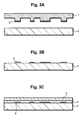
- Figs. 3A, 3B and 3C diagrammatically show respective elements of the structure for explaining the sequential process steps for fabricating an optical disk of a first embodiment according to the invention.
- numeral 1 represents a stamper as a master or mother disk which is prepared by nickel-plating a board in which data, etc. is recorded.
- This stamper is prepared using the same processes as those used in the conventional method explained above.
- a pit 2 which is of carbon particles is applied and attached on a projected portion of the stamper as shown in Fig. 3A.
- the stamper 1 is pressed against a transparent plate 3
- the pit 2 is transferred onto a surface of the transparent plate 3 as shown in Fig. 3B.
- each of the carbon particles constituting the pit 2 it is generally considered that the smaller the better (for example, 100 Angstroms). However, in the case where the carbon particles are extremely fine, they tend to be coagulated and be non-uniform so that a desirable diameter is in the order of 100 - 500 Angstroms.
- the transparent plate 3 which constitutes the optical disk is generally formed of materials such as polycarbonate, glass or polyolefin, and acrylics.
- a reflective film 4 formed on the pit generally employs an aluminum alloy. Further, a protective layer 5 formed on the reflective film 4 employs ultraviolet curing resin of an acrylic or urethane type.
- the optical disk is fabricated using the completed stamper 1 as the master or mother disk.
- the first step is to apply and attach the carbon particles onto the surface of each of the projected portion of the stamper 1.
- the carbon particles may be dispersed in a binder containing an organic solvent. This ensures the uniform attachment of the carbon particles on the stamper 1.
- the stamper 1 in the above state is pressed against the transparent plate 3 whereby the carbon particles are transferred onto the transparent plate 3 and the pit 2 is formed on the surface of the transparent plate 3.
- a reflective film 4 is formed by sputtering the aluminum alloy using the same method as used in the conventional method.
- a protective layer 5 of ultraviolet curing resin is applied by using a spin coater, and the disk is completed when the ultraviolet resin is cured.
- label printing such as for titles is made on a surface of the protective layer 5.
- optical disk on which the pit is formed as above it is possible to carry out the reproduction by using the contrast between the reflective film formed of, for example, aluminum on the disk and the pit formed of carbon particles, that is, the difference in the reflectivities between the reflective film and the pit, without using the phase difference which results from physical undulations as in the conventional optical disk.
- the fabrication method of this embodiment it is possible to fabricate a replica disk without changing the conventional fabrication method and at a higher speed than in the conventional fabrication method, and it is also possible to obtain the recording of a higher density because the pit is not formed by physical undulations but only by the particles attached.
- the undulation structure is used for the pits as in the conventional optical disk
- the present invention overcomes this problem and can utilize the same light source as used for the conventional optical disk.
- FIG. 4A and 4B diagrammatically show elements constituting the structure for use in explaining the sequential process steps of the fabrication method.
- the process in order to carry out a process in which the pit transferred onto the transparent plate is more securely adhered thereon, the process employs magnetic particles and electromagnet means during the pit formation.
- the fine particles tend to be coagulated so as to form masses thereof, and a technique available to prevent this problem is a method wherein the particles are dispersed in a binder.
- This is an area in which extensive know-how is involved and special manufacturing techniques are required.
- use of the magnetic particles, especially iron oxides (Fe204 or ⁇ -hematite Fe304) has been known since comparatively long ago, and has been confirmed as being useful for purposes of the uniformity.
- the magnetic particles have been in use in fields such as high polymer films typically represented by polyester films.
- a process is available wherein a recording material in which a fine particle of iron oxide with a diameter less than 1 ⁇ m is stably dispersed in industrial application without being coagulated is uniformly applied on high polymer films typically represented by polyester films.
- the magnetic field is provided, through an electromagnet 6, on the stamper 1 formed of nickel which is a ferromagnetic material, and the pit 2a formed by uniformly distributed magnetic particles are attracted to and adhered once on the stamper side (state shown in Fig. 4A). Then, the magnetic field is provided from the side of a transparent plate 3 through an electromagnet 7 and at the same time the stamper 1 is demagnetized, so that the pit 2a formed of the magnetic particles on the stamper 1 are attracted to and transferred on the surface of the transparent plate 3 (state shown in Fig. 4B).
- the binder (not shown) in which the magnetic particles have been dispersed through the electromagnet 6 is attracted to and attached on the projected portion of the stamper. Then, the magnetic particles on the projected portion are pressed against the transparent plate 3 with a magnetic field through an electromagnet 7 being applied from the opposite direction, and this ensures the unfailing formation of the pit 2a on the transparent plate 3 by the magnetic particles.
- the uniform magnetic particles are transferred as pits 21 on the transparent plate 3.
- the reflective film and the protective layer are formed using the same procedures as used for the first embodiment.
- a vacuum thin film formation technique such as a sputtering technique is used following the exposure process, so that a nickel alloy of about 300 ⁇ m is formed by a casting process (electro-casting). It is preferable that surfaces of the inner and outer peripheries and the back of the stamper be subjected to suitable finishing processes.
Landscapes
- Engineering & Computer Science (AREA)
- Manufacturing & Machinery (AREA)
- Manufacturing Optical Record Carriers (AREA)
- Optical Record Carriers And Manufacture Thereof (AREA)
- Exposure Of Semiconductors, Excluding Electron Or Ion Beam Exposure (AREA)
Claims (8)
- Disque optique comprenant :caractérisé en ce que les marques se composent de particules de carbone.un film réflecteur (4) qui comporte une première réflexivité ; etune pluralité de marques (2) sur lesquelles est formé ledit film réflecteur, lesdites marques se composant d'un matériau qui a une seconde réflexivité différente de ladite première réflexivité du film réflecteur,
- Disque optique selon la revendication 1, dans lequel chacune desdites particules de carbone a un diamètre de 100 à 500 Angströms.
- Disque optique comprenant :un film réflecteur (4) qui comporte une première réflexivité ; etune pluralité de marques (2) sur lesquelles est formé ledit film réflecteur, lesdites marques se composant d'un matériau qui a une seconde réflexivité différente de ladite première réflexivité du film réflecteur, caractérisé en ce que lesdites marques se composent de particules magnétiques
- Disque optique selon la revendication 3 dans lequel lesdites particules sont des particules d'oxyde de fer.
- Procédé de fabrication d'un disque optique qui comprend un film réflecteur (4) ayant une première réflexivité, et une pluralité de marques (2) de particules formées d'un matériau ayant une seconde réflexivité différente de ladite première réflexivité du film réflecteur, ledit procédé étant caractérisé par les étapes de :fixation desdites particules sur une partie en saillie d'une matrice (1) ;formation d'une réplique de disque par étapes dans lesquelles ladite matrice est mise en contact avec une surface d'une plaque transparente (3) du disque optique et dans laquelle lesdites particules sont transférées sur ladite plaque transparente, ce qui forme des marques sur ladite plaque transparente ; etformation dudit film réflecteur sur ladite réplique de disque.
- Procédé de fabrication d'un disque optique selon la revendication 5 incluant une étape dans laquelle lesdites particules sont réparties dans un liant contenant un solvant organique.
- Procédé de fabrication d'un disque optique qui comprend un film réflecteur (4) comportant une première réflexivité, et une pluralité de marques (2) de particules se composant d'un matériau ayant une seconde réflexivité différente de ladite première réflexivité du film réflecteur, lesdites particules étant des particules magnétiques, ledit procédé étant caractérisé par les étapes de :application d'un champ magnétique sur une matrice (1), ce qui provoque l'attraction et l'adhérence desdites particules magnétiques sur une partie en saillie de ladite matrice ;formation d'une réplique de disque par étapes dans lesquelles ladite matrice est mise en contact avec une surface d'une plaque transparente (3) du disque optique et dans lesquelles lesdites particules magnétiques sont transférées sur ladite plaque transparente en raison du champ magnétique, ce qui forme des marques sur ladite plaque transparente ; etformation dudit film réflecteur sur ladite réplique de disque.
- Procédé de fabrication d'un disque optique selon la revendication 7 qui comprend une étape dans laquelle lesdites particules sont réparties dans un liant contenant un solvant organique.
Applications Claiming Priority (3)
| Application Number | Priority Date | Filing Date | Title |
|---|---|---|---|
| JP338875/94 | 1994-12-27 | ||
| JP33887594 | 1994-12-27 | ||
| JP6338875A JPH08180457A (ja) | 1994-12-27 | 1994-12-27 | 光ディスク及びその製造方法 |
Publications (2)
| Publication Number | Publication Date |
|---|---|
| EP0720160A1 EP0720160A1 (fr) | 1996-07-03 |
| EP0720160B1 true EP0720160B1 (fr) | 2002-03-20 |
Family
ID=18322218
Family Applications (1)
| Application Number | Title | Priority Date | Filing Date |
|---|---|---|---|
| EP19950120611 Expired - Lifetime EP0720160B1 (fr) | 1994-12-27 | 1995-12-27 | Disque optique à marques formé par une matrice et son procédé de fabrication |
Country Status (3)
| Country | Link |
|---|---|
| EP (1) | EP0720160B1 (fr) |
| JP (1) | JPH08180457A (fr) |
| DE (1) | DE69525917T2 (fr) |
Families Citing this family (5)
| Publication number | Priority date | Publication date | Assignee | Title |
|---|---|---|---|---|
| US6873087B1 (en) * | 1999-10-29 | 2005-03-29 | Board Of Regents, The University Of Texas System | High precision orientation alignment and gap control stages for imprint lithography processes |
| JP4719464B2 (ja) * | 2002-05-08 | 2011-07-06 | エージェンシー フォー サイエンス,テクノロジー アンド リサーチ | マイクロ/ナノ構造を基板上にインプリントする方法 |
| US7828620B2 (en) | 2003-01-09 | 2010-11-09 | Sony Corporation | Method of manufacturing tubular carbon molecule and tubular carbon molecule, method of manufacturing field electron emission device and field electron emission device, and method of manufacturing display unit and display unit |
| CN101223585A (zh) * | 2005-07-21 | 2008-07-16 | Nxp股份有限公司 | 磁性rom信息载体 |
| JP4909219B2 (ja) * | 2007-09-19 | 2012-04-04 | 日本電信電話株式会社 | 微細構造作製方法 |
Family Cites Families (8)
| Publication number | Priority date | Publication date | Assignee | Title |
|---|---|---|---|---|
| US4342714A (en) * | 1981-03-31 | 1982-08-03 | Gregg David P | Process for making video discs |
| JPS60208289A (ja) * | 1984-03-31 | 1985-10-19 | Dainippon Printing Co Ltd | 光記録材料 |
| US4762770A (en) * | 1986-04-23 | 1988-08-09 | Drexler Technology Corporation | High contrast optical memory disk |
| AU607943B2 (en) * | 1987-01-24 | 1991-03-21 | Dai Nippon Insatsu Kabushiki Kaisha | Optical recording members and production thereof |
| JPS63302436A (ja) * | 1987-01-24 | 1988-12-09 | Dainippon Printing Co Ltd | 光記録体およびその製造方法 |
| JPH02116038A (ja) * | 1988-10-24 | 1990-04-27 | Nec Corp | 光ディスク |
| JPH02183441A (ja) * | 1989-01-09 | 1990-07-18 | Nec Corp | 光ディスク |
| JPH03178048A (ja) * | 1989-12-06 | 1991-08-02 | Hitachi Maxell Ltd | 光再生情報記録媒体 |
-
1994
- 1994-12-27 JP JP6338875A patent/JPH08180457A/ja active Pending
-
1995
- 1995-12-27 EP EP19950120611 patent/EP0720160B1/fr not_active Expired - Lifetime
- 1995-12-27 DE DE1995625917 patent/DE69525917T2/de not_active Expired - Fee Related
Also Published As
| Publication number | Publication date |
|---|---|
| EP0720160A1 (fr) | 1996-07-03 |
| JPH08180457A (ja) | 1996-07-12 |
| DE69525917T2 (de) | 2002-11-14 |
| DE69525917D1 (de) | 2002-04-25 |
Similar Documents
| Publication | Publication Date | Title |
|---|---|---|
| CA1225467A (fr) | Methode de fabrication d'elements de memoire optique | |
| US20070222096A1 (en) | Apparatus and Method for Manufacturing Pre-Formatted Linear Optical Data Storage Medium | |
| JPH08203126A (ja) | 光学的情報記録媒体ならびに光学的情報再生方法および 光学的情報記録再生消去方法 | |
| JPS619848A (ja) | 光記録媒体の案内溝形成方法 | |
| EP0720160A1 (fr) | Disque optique à marques formé par une matrice et son procédé de fabrication | |
| JP2000036135A (ja) | 多層情報記録媒体の製造方法 | |
| JP2001023243A (ja) | 情報記録担体及び情報記録担体再生装置 | |
| JPH01158640A (ja) | 光ディスクの製造方法 | |
| JPS62273634A (ja) | 光方式情報記録再生用テ−プおよびそれを使用する方法 | |
| JP2963516B2 (ja) | 光学的情報記録媒体用基板およびその製造方法 | |
| JPH10334518A (ja) | 光ディスク及びスタンパー | |
| KR100207701B1 (ko) | 광디스크 제조방법 | |
| JPS6151634A (ja) | 光学式情報記録媒体の製造方法 | |
| JPS605437A (ja) | 光学記録媒体 | |
| JPH01229439A (ja) | 光学的記録媒体及びその製造方法 | |
| JPH0554393A (ja) | 情報記録媒体およびその駆動装置 | |
| JPH1097735A (ja) | 光学的情報記録媒体 | |
| JPH1074341A (ja) | 光学記録媒体の製造方法 | |
| JPH04146539A (ja) | 光ディスク | |
| EP0142927A2 (fr) | Disque optique | |
| JPH0963123A (ja) | 多層光学記録媒体 | |
| JPH09265661A (ja) | 記録媒体およびその製造方法 | |
| JPH03187036A (ja) | 光カード及び光カードの製造方法 | |
| JPS60197960A (ja) | 光メモリ素子の製造方法 | |
| JPH04162224A (ja) | 光ディスク |
Legal Events
| Date | Code | Title | Description |
|---|---|---|---|
| PUAI | Public reference made under article 153(3) epc to a published international application that has entered the european phase |
Free format text: ORIGINAL CODE: 0009012 |
|
| AK | Designated contracting states |
Kind code of ref document: A1 Designated state(s): DE GB NL |
|
| 17P | Request for examination filed |
Effective date: 19960906 |
|
| 17Q | First examination report despatched |
Effective date: 19990714 |
|
| GRAG | Despatch of communication of intention to grant |
Free format text: ORIGINAL CODE: EPIDOS AGRA |
|
| GRAG | Despatch of communication of intention to grant |
Free format text: ORIGINAL CODE: EPIDOS AGRA |
|
| GRAH | Despatch of communication of intention to grant a patent |
Free format text: ORIGINAL CODE: EPIDOS IGRA |
|
| GRAH | Despatch of communication of intention to grant a patent |
Free format text: ORIGINAL CODE: EPIDOS IGRA |
|
| REG | Reference to a national code |
Ref country code: GB Ref legal event code: IF02 |
|
| GRAA | (expected) grant |
Free format text: ORIGINAL CODE: 0009210 |
|
| AK | Designated contracting states |
Kind code of ref document: B1 Designated state(s): DE GB NL |
|
| REF | Corresponds to: |
Ref document number: 69525917 Country of ref document: DE Date of ref document: 20020425 |
|
| PLBE | No opposition filed within time limit |
Free format text: ORIGINAL CODE: 0009261 |
|
| STAA | Information on the status of an ep patent application or granted ep patent |
Free format text: STATUS: NO OPPOSITION FILED WITHIN TIME LIMIT |
|
| 26N | No opposition filed |
Effective date: 20021223 |
|
| PGFP | Annual fee paid to national office [announced via postgrant information from national office to epo] |
Ref country code: NL Payment date: 20081215 Year of fee payment: 14 |
|
| PGFP | Annual fee paid to national office [announced via postgrant information from national office to epo] |
Ref country code: DE Payment date: 20081229 Year of fee payment: 14 |
|
| PGFP | Annual fee paid to national office [announced via postgrant information from national office to epo] |
Ref country code: GB Payment date: 20081224 Year of fee payment: 14 |
|
| REG | Reference to a national code |
Ref country code: NL Ref legal event code: V1 Effective date: 20100701 |
|
| GBPC | Gb: european patent ceased through non-payment of renewal fee |
Effective date: 20091227 |
|
| PG25 | Lapsed in a contracting state [announced via postgrant information from national office to epo] |
Ref country code: NL Free format text: LAPSE BECAUSE OF NON-PAYMENT OF DUE FEES Effective date: 20100701 |
|
| PG25 | Lapsed in a contracting state [announced via postgrant information from national office to epo] |
Ref country code: DE Free format text: LAPSE BECAUSE OF NON-PAYMENT OF DUE FEES Effective date: 20100701 |
|
| PG25 | Lapsed in a contracting state [announced via postgrant information from national office to epo] |
Ref country code: GB Free format text: LAPSE BECAUSE OF NON-PAYMENT OF DUE FEES Effective date: 20091227 |