EP0528367A1 - Dreidimensionaler Mehrchip-Modul - Google Patents
Dreidimensionaler Mehrchip-Modul Download PDFInfo
- Publication number
- EP0528367A1 EP0528367A1 EP92113849A EP92113849A EP0528367A1 EP 0528367 A1 EP0528367 A1 EP 0528367A1 EP 92113849 A EP92113849 A EP 92113849A EP 92113849 A EP92113849 A EP 92113849A EP 0528367 A1 EP0528367 A1 EP 0528367A1
- Authority
- EP
- European Patent Office
- Prior art keywords
- substrate
- chip module
- recited
- electrode terminals
- heat conductive
- Prior art date
- Legal status (The legal status is an assumption and is not a legal conclusion. Google has not performed a legal analysis and makes no representation as to the accuracy of the status listed.)
- Withdrawn
Links
Images
Classifications
-
- H—ELECTRICITY
- H10—SEMICONDUCTOR DEVICES; ELECTRIC SOLID-STATE DEVICES NOT OTHERWISE PROVIDED FOR
- H10W—GENERIC PACKAGES, INTERCONNECTIONS, CONNECTORS OR OTHER CONSTRUCTIONAL DETAILS OF DEVICES COVERED BY CLASS H10
- H10W40/00—Arrangements for thermal protection or thermal control
- H10W40/20—Arrangements for cooling
- H10W40/22—Arrangements for cooling characterised by their shape, e.g. having conical or cylindrical projections
-
- H—ELECTRICITY
- H10—SEMICONDUCTOR DEVICES; ELECTRIC SOLID-STATE DEVICES NOT OTHERWISE PROVIDED FOR
- H10W—GENERIC PACKAGES, INTERCONNECTIONS, CONNECTORS OR OTHER CONSTRUCTIONAL DETAILS OF DEVICES COVERED BY CLASS H10
- H10W90/00—Package configurations
-
- H—ELECTRICITY
- H10—SEMICONDUCTOR DEVICES; ELECTRIC SOLID-STATE DEVICES NOT OTHERWISE PROVIDED FOR
- H10W—GENERIC PACKAGES, INTERCONNECTIONS, CONNECTORS OR OTHER CONSTRUCTIONAL DETAILS OF DEVICES COVERED BY CLASS H10
- H10W72/00—Interconnections or connectors in packages
- H10W72/851—Dispositions of multiple connectors or interconnections
- H10W72/874—On different surfaces
- H10W72/877—Bump connectors and die-attach connectors
-
- H—ELECTRICITY
- H10—SEMICONDUCTOR DEVICES; ELECTRIC SOLID-STATE DEVICES NOT OTHERWISE PROVIDED FOR
- H10W—GENERIC PACKAGES, INTERCONNECTIONS, CONNECTORS OR OTHER CONSTRUCTIONAL DETAILS OF DEVICES COVERED BY CLASS H10
- H10W72/00—Interconnections or connectors in packages
- H10W72/851—Dispositions of multiple connectors or interconnections
- H10W72/874—On different surfaces
- H10W72/884—Die-attach connectors and bond wires
-
- H—ELECTRICITY
- H10—SEMICONDUCTOR DEVICES; ELECTRIC SOLID-STATE DEVICES NOT OTHERWISE PROVIDED FOR
- H10W—GENERIC PACKAGES, INTERCONNECTIONS, CONNECTORS OR OTHER CONSTRUCTIONAL DETAILS OF DEVICES COVERED BY CLASS H10
- H10W90/00—Package configurations
- H10W90/20—Configurations of stacked chips
-
- H—ELECTRICITY
- H10—SEMICONDUCTOR DEVICES; ELECTRIC SOLID-STATE DEVICES NOT OTHERWISE PROVIDED FOR
- H10W—GENERIC PACKAGES, INTERCONNECTIONS, CONNECTORS OR OTHER CONSTRUCTIONAL DETAILS OF DEVICES COVERED BY CLASS H10
- H10W90/00—Package configurations
- H10W90/20—Configurations of stacked chips
- H10W90/22—Configurations of stacked chips the stacked chips being on both top and bottom sides of a package substrate, interposer or RDL
-
- H—ELECTRICITY
- H10—SEMICONDUCTOR DEVICES; ELECTRIC SOLID-STATE DEVICES NOT OTHERWISE PROVIDED FOR
- H10W—GENERIC PACKAGES, INTERCONNECTIONS, CONNECTORS OR OTHER CONSTRUCTIONAL DETAILS OF DEVICES COVERED BY CLASS H10
- H10W90/00—Package configurations
- H10W90/20—Configurations of stacked chips
- H10W90/288—Configurations of stacked chips characterised by arrangements for thermal management of the stacked chips
-
- H—ELECTRICITY
- H10—SEMICONDUCTOR DEVICES; ELECTRIC SOLID-STATE DEVICES NOT OTHERWISE PROVIDED FOR
- H10W—GENERIC PACKAGES, INTERCONNECTIONS, CONNECTORS OR OTHER CONSTRUCTIONAL DETAILS OF DEVICES COVERED BY CLASS H10
- H10W90/00—Package configurations
- H10W90/701—Package configurations characterised by the relative positions of pads or connectors relative to package parts
- H10W90/721—Package configurations characterised by the relative positions of pads or connectors relative to package parts of bump connectors
- H10W90/724—Package configurations characterised by the relative positions of pads or connectors relative to package parts of bump connectors between a chip and a stacked insulating package substrate, interposer or RDL
-
- H—ELECTRICITY
- H10—SEMICONDUCTOR DEVICES; ELECTRIC SOLID-STATE DEVICES NOT OTHERWISE PROVIDED FOR
- H10W—GENERIC PACKAGES, INTERCONNECTIONS, CONNECTORS OR OTHER CONSTRUCTIONAL DETAILS OF DEVICES COVERED BY CLASS H10
- H10W90/00—Package configurations
- H10W90/701—Package configurations characterised by the relative positions of pads or connectors relative to package parts
- H10W90/751—Package configurations characterised by the relative positions of pads or connectors relative to package parts of bond wires
- H10W90/754—Package configurations characterised by the relative positions of pads or connectors relative to package parts of bond wires between a chip and a stacked insulating package substrate, interposer or RDL
Definitions
- the present invention relates to a three-dimensional multi-chip module comprising a plurality of semiconductor chips, and more particularly to the structure of a multi-chip module which achieves a higher integration density and a high power output.
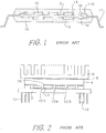
- FIG. 1 A plurality of semiconductor elements (chips) 10 are arranged on both surfaces of a substrate 2. Wiring patterns and electrode terminals (not shown) are formed in advance on the surfaces of the substrate 2, and bonding pads formed on each semiconductor element 10 are operatively connected to electrode terminals of the wiring patterns by bonding wires 13.
- the substrate 2 with semiconductor elements 10 is disposed on a stage 11a of a lead frame 11, and electrode terminals of the wiring pattern are operatively connected by boding wires 15 to inner leads 11b of the lead frame 11.
- boding wires 15 to inner leads 11b of the lead frame 11.
- a wireless bonding method In order to obtain a higher integration density in a multi-chip module, a wireless bonding method has been utilized.
- a flip-chip method As the wireless bonding method, a flip-chip method, a beam lead method and a TAB (tape automated bonding) method are widely known.
- the flip-chip method is most effective for saving bonding area on the surface of a substrate.
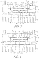
- FIG. 2 shows an example of a multi-chip module of the prior art, in which the multi-chip module comprises two high output power semiconductor elements 10a.
- the multi-chip module further comprises two semiconductor elements 10b heat dissipation of which is comparatively small.
- All semiconductor elements 10a, 10b are bonded facedown to a substrate 2 by the flip-chip bonding method, namely, bumps 14 of solder are formed in advance on the major surface of the semiconductor elements and the semiconductor elements are disposed on the substrate 2, thereby the bumps on the major surface being brought in contact with electrode terminals of wiring pattern (not shown) on the substrate 2 and bonded together, and the wiring pattern being connected to outer leads 12.
- the back surface of the high power semiconductor elements 10a is further made in contact with a heat conductive base 4 using heat conductive paste 16 therebetween. After fixing a heat sink 5 to the above package, the multi-chip module is finally completed.
- the package structure of the prior art of Figure 2 encloses semiconductor elements which are arranged two-dimensionally on a front surface of the substrate 2 only. Therefore, an integration density can not be increased to the level of three-dimensional multi-chip module. Further, there is a problem that mixed disposition of the semiconductor elements is difficult, in which one semiconductor element requires wire bonding and the other semiconductor element requires flip-chip bonding.
- a three-dimensional multi-chip module of the present invention comprising: a substrate having a first and second surface, and comprising wiring patterns having a plurality of electrode terminals on the first and second surfaces respectively, at least a single semiconductor element arranged facedown on the first surface of the substrate and operatively connected to the electrode terminals on the first surface, at least a single semiconductor element and/or passive element arranged on the second surface of the substrate and operatively connected to the electrode terminals on the second surface, and a heat conductive base facing the first surface of the substrate and thermally in contact with the back surface of the semiconductor element arranged on the first surface of the substrate.
- the multi-chip module of the present invention further comprises a support base and a cap, forming an enclosure together with the heat conductive base, and a heat sink fixed to the heat conductive base, which results in achieving a high integration density and a high power of the module.
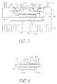
- Figure 3 shows a schematic cross section of an embodiment of a three-dimensional multi-chip module in accordance with the present invention.
- a support base 3, a heat conductive base 4 and a cap 7 form a packaging enclosure of the multi-chip module, and a substrate 2 with semiconductor elements 10a, 10b is enclosed therein.
- a heat sink 5 is attached to the heat conductive base 4 and enhances heat handling capability of the multi-chip module.
- the substrate 2 is made of multilayer ceramic and predetermined wiring patterns are formed between ceramic layers and/or on the surface of the substrate by the known technology.
- a plurality of semiconductor elements 10a, 10b are arranged on a first and second surface of the substrate 2, thereby the first surface being defined for the surface which subsequently faces the heat conductive base 4 after packaging.
- the semiconductor element 10a which requires comparatively large heat dissipation is arranged on the first surface of the substrate 2, and the semiconductor element 10b which requires comparatively small heat dissipation is arranged on the second surface thereof. Therefore, a semiconductor element which dissipates several watts to tens of watts is preferably arranged on the first surface of the substrate 2.
- both semiconductor elements 10a, 10b are bonded facedown to the first and second surfaces of the substrate 2, namely, the major surface comprising main integrated circuits of the semiconductor element is bonded facing the substrate 2.
- a flip-chip method is applied for bonding the semiconductor elements 10a, 10b and, in this case, a plurality of bumps 14 which are to be bonded to electrode terminals of the wiring pattern, are formed in advance on the major surface of the semiconductor elements.
- the semiconductor elements 10a, 10b are disposed at the predetermined positions respectively on the first and second surfaces of the substrate 2 and they are heated for reflowing the solder of the bumps.
- a subassembly composed of the semiconductor elements 10a, 10b and the substrate 2 is mounted on another subassembly composed of the support base 3 and the heat conductive base 4, thereby these two parts being fixed together by thermal conductive resin or solder.
- the support base 3 is made of multilayer ceramic and comprises a buried wiring pattern (not shown) and a plurality of outer leads 12 and a plurality of electrode terminals 31. The outer leads 12 and electrode terminals 31 are operatively connected by the wiring pattern.
- the material used for the heat conductive base 4 is required to have a high thermal conductivity and also have a thermal expansion coefficient which is close to that of silicon as much as possible.
- Porous sintered copper-tungsten (Cu-W) and sintered copper-molybdenum (Cu-Mo) have a thermal expansion coefficient of approx. 6x10 ⁇ 6/deg, and these materials are favorable as the heat conductive base 4 on which silicon chip (having a thermal expansion coefficient of about 2.6x10 ⁇ 6/deg) is disposed.
- the substrate 2 with semiconductor elements 10a, 10b is mounted on the heat conductive base 4 in a manner that the minor surfaces (back surfaces) of the semiconductor elements 10a are fixed to the heat conductive base 4 using heat conductive adhesive 16 such as Ag paste, solder, etc. between the thermal conductive base 4 and the minor surface of the semiconductor elements 10a, and further the substrate 2 is fixed to the support base 3 using insulating thermal conductive resin therebetween.
- heat conductive adhesive 16 such as Ag paste, solder, etc.
- electrode terminals 31 on the step portion of the support base 3 and electrode terminals 21 on the substrate 2 are connected by bonding wires 15.
- a heat sink 5 of aluminum or aluminum alloy is fixed on the outer surface of the heat conductive base 4 using thermal compound, and the cap 7 of iron-nickel alloy closes an opening of the support base 3.
- Figure 4 shows a schematic cross section of another embodiment of a three-dimensional multi-chip module of the present invention.
- Semiconductor elements 10a having comparatively a large heat dissipation are arranged facedown on the first surface (bottom surface) of the substrate 2 and bonded thereto in the same way as in Figure 3.
- semiconductor elements 10b having comparatively a small heat dissipation are arranged faceup on the second surface (front surface) of the substrate 2, and pads (not shown) on the semiconductor element 10b are connected to electrode terminals on the substrate 2 using a bonding wire 13.
- a passive elements 6 such as capacitor, coil, and resistor are arranged on the second surface of the substrate 2 and connected to the electrode terminals on the substrate 2.
- Figure 4 shows that active and/or passive elements which require a wire-bonding method can be mixed and comprised in the module using the second surface of the substrate 2.
- Figure 5 shows a schematic cross section of still another embodiment of the present invention.
- the module of Figure 5 further comprises a heat conductive metal member 9 having elasticity.
- One end 9a of the metal member 9 is fixed to an inside surface of the cap 7.
- the other end 9b of the metal member 9 is elastically in contact with the inside surface of the cap 7 and can move when the metal member 9 is subjected to thermal expansion.
- the middle portion of the metal member 9 is elastically in contact with the second surface of the substrate 2 and pressing the second surface of the substrate 2 when the cap 7 closes the opening of the support base 3.
- semiconductor elements 10b and/or passive elements 6 arranged on the second surface of the substrate 2 have no direct heat removing means such as the heat conductive base 4 for the semiconductor elements 10a on the first surface of the substrate 2, heats generated in semiconductor elements 10b and passive elements 6 are conducted to the substrate 2. Temperature rise of the substrate 2 can be remarkably reduced by the function of the above metal member 9 by conducting the heat of the substrate 2 to the cap 7 which is cooled by the ambient atmosphere.
- the shape of the metal member 9 in Figure 5 shows an illustrative one, and many other shapes can be used.
- One end of the metal member 9 may be fixed to the substrate 2 and the other end may be in contact with the cap 7 or vice versa, thereby metal member 9 having a "U" character shape being used laying its side up.
- Figure 6 shows a schematic cross section of a modified structure of a substrate 2 with semiconductor elements 10a, 10b arranged thereon.
- Wiring patterns (not shown) on the substrate 2 has test terminals 22 other than electrode terminals 21 which are actually used for bonding the semiconductor elements 10a, 10b and subsequently for connecting the wiring patterns to the outside electrode terminals.
- the subassembly of Figure 6 comprising the substrate 2 and the semiconductor elements 10a, 10b bonded thereto, is subjected to function test, in which the entire circuit of the module is divided into several circuit blocks and each circuit block is tested using the test terminals 22 and/or electrode terminals 21.
- the substrate 2 with semiconductor elements 10a, 10b is packaged in the enclosure of support base 3, heat conductive base 4 and cap 7.
- all semiconductor elements 10a, 10b are bonded facedown to the substrate 2 using bumps 14.
- a substrate 2 having test terminals 22 can be utilized for other multi-chip module comprising semiconductor elements requiring wire bonding and/or passive elements.
Landscapes
- Cooling Or The Like Of Semiconductors Or Solid State Devices (AREA)
Applications Claiming Priority (2)
| Application Number | Priority Date | Filing Date | Title |
|---|---|---|---|
| JP3202089A JPH0548000A (ja) | 1991-08-13 | 1991-08-13 | 半導体装置 |
| JP202089/91 | 1991-08-13 |
Publications (1)
| Publication Number | Publication Date |
|---|---|
| EP0528367A1 true EP0528367A1 (de) | 1993-02-24 |
Family
ID=16451786
Family Applications (1)
| Application Number | Title | Priority Date | Filing Date |
|---|---|---|---|
| EP92113849A Withdrawn EP0528367A1 (de) | 1991-08-13 | 1992-08-13 | Dreidimensionaler Mehrchip-Modul |
Country Status (4)
| Country | Link |
|---|---|
| US (1) | US5297006A (de) |
| EP (1) | EP0528367A1 (de) |
| JP (1) | JPH0548000A (de) |
| KR (1) | KR930005177A (de) |
Cited By (18)
| Publication number | Priority date | Publication date | Assignee | Title |
|---|---|---|---|---|
| EP0694968A3 (de) * | 1994-07-26 | 1996-09-11 | Nec Corp | Halbleiter-Multichip-Baustein |
| EP0792517A4 (de) * | 1994-11-15 | 1998-06-24 | Formfactor Inc | Elektrische kontaktstruktur aus flexiblem draht |
| EP0729652A4 (de) * | 1993-11-16 | 1998-06-24 | Formfactor Inc | Kontakstruktur für verbindungen, zwischenstück, halbleiteranordnung und verfahren |
| US6049976A (en) | 1993-11-16 | 2000-04-18 | Formfactor, Inc. | Method of mounting free-standing resilient electrical contact structures to electronic components |
| EP0996155A3 (de) * | 1998-10-23 | 2001-04-18 | Sony Corporation | Vorrichtung mit integrierter Schaltung für Hochfrequenz |
| US6336269B1 (en) | 1993-11-16 | 2002-01-08 | Benjamin N. Eldridge | Method of fabricating an interconnection element |
| US6727579B1 (en) | 1994-11-16 | 2004-04-27 | Formfactor, Inc. | Electrical contact structures formed by configuring a flexible wire to have a springable shape and overcoating the wire with at least one layer of a resilient conductive material, methods of mounting the contact structures to electronic components, and applications for employing the contact structures |
| US6778406B2 (en) | 1993-11-16 | 2004-08-17 | Formfactor, Inc. | Resilient contact structures for interconnecting electronic devices |
| WO2004061861A3 (en) * | 2002-12-31 | 2004-10-28 | Matrix Semiconductor Inc | Nand memory array incorporating capacitance boosting of channel regions in unselected memory cells and method for operation of same |
| US7005350B2 (en) | 2002-12-31 | 2006-02-28 | Matrix Semiconductor, Inc. | Method for fabricating programmable memory array structures incorporating series-connected transistor strings |
| US7023739B2 (en) | 2003-12-05 | 2006-04-04 | Matrix Semiconductor, Inc. | NAND memory array incorporating multiple write pulse programming of individual memory cells and method for operation of same |
| US7084656B1 (en) | 1993-11-16 | 2006-08-01 | Formfactor, Inc. | Probe for semiconductor devices |
| US7200930B2 (en) | 1994-11-15 | 2007-04-10 | Formfactor, Inc. | Probe for semiconductor devices |
| US7221588B2 (en) | 2003-12-05 | 2007-05-22 | Sandisk 3D Llc | Memory array incorporating memory cells arranged in NAND strings |
| US7233522B2 (en) | 2002-12-31 | 2007-06-19 | Sandisk 3D Llc | NAND memory array incorporating capacitance boosting of channel regions in unselected memory cells and method for operation of same |
| US7505321B2 (en) | 2002-12-31 | 2009-03-17 | Sandisk 3D Llc | Programmable memory array structure incorporating series-connected transistor strings and methods for fabrication and operation of same |
| US8485418B2 (en) | 1995-05-26 | 2013-07-16 | Formfactor, Inc. | Method of wirebonding that utilizes a gas flow within a capillary from which a wire is played out |
| CN112420636A (zh) * | 2020-11-19 | 2021-02-26 | 四川长虹空调有限公司 | 芯片散热结构 |
Families Citing this family (55)
| Publication number | Priority date | Publication date | Assignee | Title |
|---|---|---|---|---|
| JPH0786717A (ja) * | 1993-09-17 | 1995-03-31 | Fujitsu Ltd | プリント配線板構造体 |
| US5772451A (en) | 1993-11-16 | 1998-06-30 | Form Factor, Inc. | Sockets for electronic components and methods of connecting to electronic components |
| JPH07202463A (ja) * | 1994-01-11 | 1995-08-04 | Yokogawa Electric Corp | 電子回路モジュール |
| AT402135B (de) * | 1994-03-30 | 1997-02-25 | Electrovac | Schaltungsträger |
| EP0717443B1 (de) * | 1994-07-04 | 1999-03-03 | Matsushita Electric Industrial Co., Ltd. | Integrierte halbleiteranordnung |
| EP0693776B1 (de) * | 1994-07-15 | 2000-05-31 | Mitsubishi Materials Corporation | Keramik-Gehäuse mit hoher Wärmeabstrahlung |
| JPH0846136A (ja) * | 1994-07-26 | 1996-02-16 | Fujitsu Ltd | 半導体装置 |
| US6031723A (en) * | 1994-08-18 | 2000-02-29 | Allen-Bradley Company, Llc | Insulated surface mount circuit board construction |
| JP2636777B2 (ja) * | 1995-02-14 | 1997-07-30 | 日本電気株式会社 | マイクロプロセッサ用半導体モジュール |
| SE515416C2 (sv) * | 1995-02-16 | 2001-07-30 | Ericsson Telefon Ab L M | Anordning vid integrerade kretsar, och metod för dess montering |
| TW373308B (en) * | 1995-02-24 | 1999-11-01 | Agere Systems Inc | Thin packaging of multi-chip modules with enhanced thermal/power management |
| US5572405A (en) * | 1995-06-07 | 1996-11-05 | International Business Machines Corporation (Ibm) | Thermally enhanced ball grid array package |
| US5607538A (en) * | 1995-09-07 | 1997-03-04 | Ford Motor Company | Method of manufacturing a circuit assembly |
| US6008988A (en) * | 1995-12-20 | 1999-12-28 | Intel Corporation | Integrated circuit package with a heat spreader coupled to a pair of electrical devices |
| US5785535A (en) * | 1996-01-17 | 1998-07-28 | International Business Machines Corporation | Computer system with surface mount socket |
| US5729052A (en) * | 1996-06-20 | 1998-03-17 | International Business Machines Corporation | Integrated ULSI heatsink |
| US5847927A (en) * | 1997-01-27 | 1998-12-08 | Raytheon Company | Electronic assembly with porous heat exchanger and orifice plate |
| US6188874B1 (en) | 1997-06-27 | 2001-02-13 | Lockheed Martin Corporation | Control and telemetry signal communication system for geostationary satellites |
| US5990418A (en) * | 1997-07-29 | 1999-11-23 | International Business Machines Corporation | Hermetic CBGA/CCGA structure with thermal paste cooling |
| US6019166A (en) * | 1997-12-30 | 2000-02-01 | Intel Corporation | Pickup chuck with an integral heatsink |
| US5990549A (en) * | 1998-02-06 | 1999-11-23 | Intel Corporation | Thermal bus bar design for an electronic cartridge |
| US6552264B2 (en) | 1998-03-11 | 2003-04-22 | International Business Machines Corporation | High performance chip packaging and method |
| US6369444B1 (en) * | 1998-05-19 | 2002-04-09 | Agere Systems Guardian Corp. | Packaging silicon on silicon multichip modules |
| US6265771B1 (en) | 1999-01-27 | 2001-07-24 | International Business Machines Corporation | Dual chip with heat sink |
| SE516139C2 (sv) * | 1999-03-17 | 2001-11-26 | Ericsson Telefon Ab L M | Förfarande och anordning för att förbättra termiska och elektriska egenskaper hos komponenter förbunda med ett substrat monterat på en bärare |
| US6890798B2 (en) | 1999-06-08 | 2005-05-10 | Intel Corporation | Stacked chip packaging |
| DE19928733A1 (de) * | 1999-06-23 | 2001-01-04 | Giesecke & Devrient Gmbh | Halbleiterspeicher-Chipmodul |
| US6297551B1 (en) * | 1999-09-22 | 2001-10-02 | Agere Systems Guardian Corp. | Integrated circuit packages with improved EMI characteristics |
| US6473310B1 (en) * | 2000-02-18 | 2002-10-29 | Stmicroelectronics S.R.L. | Insulated power multichip package |
| EP1990832A3 (de) * | 2000-02-25 | 2010-09-29 | Ibiden Co., Ltd. | Mehrschichtige Leiterplatte und Herstellungsverfahren für mehrschichtige Leiterplatte |
| WO2002027786A1 (en) * | 2000-09-25 | 2002-04-04 | Ibiden Co., Ltd. | Semiconductor element, method of manufacturing semiconductor element, multi-layer printed circuit board, and method of manufacturing multi-layer printed circuit board |
| US6627980B2 (en) | 2001-04-12 | 2003-09-30 | Formfactor, Inc. | Stacked semiconductor device assembly with microelectronic spring contacts |
| US20050136640A1 (en) * | 2002-01-07 | 2005-06-23 | Chuan Hu | Die exhibiting an effective coefficient of thermal expansion equivalent to a substrate mounted thereon, and processes of making same |
| US6841413B2 (en) * | 2002-01-07 | 2005-01-11 | Intel Corporation | Thinned die integrated circuit package |
| TW577153B (en) * | 2002-12-31 | 2004-02-21 | Advanced Semiconductor Eng | Cavity-down MCM package |
| US6711021B1 (en) * | 2003-01-15 | 2004-03-23 | Hewlett-Packard Development Company, L.P. | Systems and methods that use at least one component to remove the heat generated by at least one other component |
| GB0304438D0 (en) * | 2003-02-27 | 2003-04-02 | Lang Andrew | Bicycle display and storage bracket |
| US7365273B2 (en) * | 2004-12-03 | 2008-04-29 | Delphi Technologies, Inc. | Thermal management of surface-mount circuit devices |
| US7310036B2 (en) | 2005-01-10 | 2007-12-18 | International Business Machines Corporation | Heat sink for integrated circuit devices |
| US7473579B2 (en) * | 2005-01-31 | 2009-01-06 | Purdue Research Foundation | Self-aligned wafer level integration system |
| DE102005053974B3 (de) * | 2005-11-11 | 2007-03-01 | Siemens Ag | Elektronische Schaltungsanordnung und Verfahren zur Herstellung einer elektronischen Schaltungsanordnung |
| US8174114B2 (en) * | 2005-12-15 | 2012-05-08 | Taiwan Semiconductor Manufacturing Go. Ltd. | Semiconductor package structure with constraint stiffener for cleaning and underfilling efficiency |
| JP4821537B2 (ja) * | 2006-09-26 | 2011-11-24 | 株式会社デンソー | 電子制御装置 |
| KR101489325B1 (ko) * | 2007-03-12 | 2015-02-06 | 페어차일드코리아반도체 주식회사 | 플립-칩 방식의 적층형 파워 모듈 및 그 파워 모듈의제조방법 |
| US20090080163A1 (en) * | 2007-05-17 | 2009-03-26 | Lockheed Martin Corporation | Printed wiring board assembly |
| US20100314730A1 (en) * | 2009-06-16 | 2010-12-16 | Broadcom Corporation | Stacked hybrid interposer through silicon via (TSV) package |
| US8680670B2 (en) | 2010-10-22 | 2014-03-25 | International Business Machines Corporation | Multi-chip module system with removable socketed modules |
| CN102891116B (zh) | 2011-07-20 | 2015-06-10 | 讯芯电子科技(中山)有限公司 | 内埋元件封装结构及制造方法 |
| US20130119529A1 (en) * | 2011-11-15 | 2013-05-16 | Taiwan Semiconductor Manufacturing Company, Ltd. | Semiconductor device having lid structure and method of making same |
| US20130277855A1 (en) * | 2012-04-24 | 2013-10-24 | Terry (Teckgyu) Kang | High density 3d package |
| KR102127335B1 (ko) * | 2012-10-29 | 2020-06-30 | 삼성전자주식회사 | 반도체 모듈 |
| ITUB20153344A1 (it) * | 2015-09-02 | 2017-03-02 | St Microelectronics Srl | Modulo di potenza elettronico con migliorata dissipazione termica e relativo metodo di fabbricazione |
| RU2656030C2 (ru) * | 2016-07-14 | 2018-05-30 | Акционерное общество "Концерн радиостроения "Вега" | Способ изготовления трехмерного электронного модуля |
| DE102018201842A1 (de) * | 2018-02-06 | 2019-08-08 | Siemens Aktiengesellschaft | Leistungselektronische Schaltung mit mehreren Leistungsmodulen |
| US11521939B2 (en) * | 2020-07-24 | 2022-12-06 | Advanced Semiconductor Engineering, Inc. | Semiconductor device structure having stiffener with two or more contact points for heat dissipating element |
Citations (2)
| Publication number | Priority date | Publication date | Assignee | Title |
|---|---|---|---|---|
| EP0264469A1 (de) * | 1986-10-21 | 1988-04-27 | International Business Machines Corporation | Anordnung zur Verdoppelung der Packungsdichte monolithisch integrierte Schaltungen enthaltender Halbleiterchips |
| FR2630859A1 (fr) * | 1988-04-27 | 1989-11-03 | Thomson Composants Militaires | Boitier ceramique multicouches a plusieurs puces de circuit-integre |
Family Cites Families (2)
| Publication number | Priority date | Publication date | Assignee | Title |
|---|---|---|---|---|
| FR2550009B1 (fr) * | 1983-07-29 | 1986-01-24 | Inf Milit Spatiale Aeronaut | Boitier de composant electronique muni d'un condensateur |
| JPS629649A (ja) * | 1985-07-08 | 1987-01-17 | Nec Corp | 半導体用パツケ−ジ |
-
1991
- 1991-08-13 JP JP3202089A patent/JPH0548000A/ja not_active Withdrawn
-
1992
- 1992-07-21 US US07/916,264 patent/US5297006A/en not_active Expired - Fee Related
- 1992-08-10 KR KR1019920014319A patent/KR930005177A/ko not_active Ceased
- 1992-08-13 EP EP92113849A patent/EP0528367A1/de not_active Withdrawn
Patent Citations (2)
| Publication number | Priority date | Publication date | Assignee | Title |
|---|---|---|---|---|
| EP0264469A1 (de) * | 1986-10-21 | 1988-04-27 | International Business Machines Corporation | Anordnung zur Verdoppelung der Packungsdichte monolithisch integrierte Schaltungen enthaltender Halbleiterchips |
| FR2630859A1 (fr) * | 1988-04-27 | 1989-11-03 | Thomson Composants Militaires | Boitier ceramique multicouches a plusieurs puces de circuit-integre |
Non-Patent Citations (1)
| Title |
|---|
| IBM TECHNICAL DISCLOSURE BULLETIN vol. 27, no. 7B, December 1984, NEW YORK page 4226 R.A.CICONE ET AL 'silicon integrated high performance package' * |
Cited By (31)
| Publication number | Priority date | Publication date | Assignee | Title |
|---|---|---|---|---|
| US7082682B2 (en) | 1993-11-16 | 2006-08-01 | Formfactor, Inc. | Contact structures and methods for making same |
| US6279227B1 (en) | 1993-11-16 | 2001-08-28 | Igor Y. Khandros | Method of forming a resilient contact structure |
| EP0729652A4 (de) * | 1993-11-16 | 1998-06-24 | Formfactor Inc | Kontakstruktur für verbindungen, zwischenstück, halbleiteranordnung und verfahren |
| US5900738A (en) * | 1993-11-16 | 1999-05-04 | Formfactor, Inc. | Contact structure device for interconnections, interposer, semiconductor assembly and package using the same and method |
| US5917707A (en) * | 1993-11-16 | 1999-06-29 | Formfactor, Inc. | Flexible contact structure with an electrically conductive shell |
| US5926951A (en) * | 1993-11-16 | 1999-07-27 | Formfactor, Inc. | Method of stacking electronic components |
| US6049976A (en) | 1993-11-16 | 2000-04-18 | Formfactor, Inc. | Method of mounting free-standing resilient electrical contact structures to electronic components |
| US6184587B1 (en) | 1993-11-16 | 2001-02-06 | Formfactor, Inc. | Resilient contact structures, electronic interconnection component, and method of mounting resilient contact structures to electronic components |
| US7084656B1 (en) | 1993-11-16 | 2006-08-01 | Formfactor, Inc. | Probe for semiconductor devices |
| US6242803B1 (en) | 1993-11-16 | 2001-06-05 | Formfactor, Inc. | Semiconductor devices with integral contact structures |
| US6274823B1 (en) | 1993-11-16 | 2001-08-14 | Formfactor, Inc. | Interconnection substrates with resilient contact structures on both sides |
| US6778406B2 (en) | 1993-11-16 | 2004-08-17 | Formfactor, Inc. | Resilient contact structures for interconnecting electronic devices |
| US6336269B1 (en) | 1993-11-16 | 2002-01-08 | Benjamin N. Eldridge | Method of fabricating an interconnection element |
| US6476333B1 (en) | 1993-11-16 | 2002-11-05 | Formfactor, Inc. | Raised contact structures (solder columns) |
| US6835898B2 (en) | 1993-11-16 | 2004-12-28 | Formfactor, Inc. | Electrical contact structures formed by configuring a flexible wire to have a springable shape and overcoating the wire with at least one layer of a resilient conductive material, methods of mounting the contact structures to electronic components, and applications for employing the contact structures |
| US7225538B2 (en) | 1993-11-16 | 2007-06-05 | Formfactor, Inc. | Resilient contact structures formed and then attached to a substrate |
| EP0694968A3 (de) * | 1994-07-26 | 1996-09-11 | Nec Corp | Halbleiter-Multichip-Baustein |
| EP0792517A4 (de) * | 1994-11-15 | 1998-06-24 | Formfactor Inc | Elektrische kontaktstruktur aus flexiblem draht |
| US7200930B2 (en) | 1994-11-15 | 2007-04-10 | Formfactor, Inc. | Probe for semiconductor devices |
| US6727579B1 (en) | 1994-11-16 | 2004-04-27 | Formfactor, Inc. | Electrical contact structures formed by configuring a flexible wire to have a springable shape and overcoating the wire with at least one layer of a resilient conductive material, methods of mounting the contact structures to electronic components, and applications for employing the contact structures |
| US8485418B2 (en) | 1995-05-26 | 2013-07-16 | Formfactor, Inc. | Method of wirebonding that utilizes a gas flow within a capillary from which a wire is played out |
| EP0996155A3 (de) * | 1998-10-23 | 2001-04-18 | Sony Corporation | Vorrichtung mit integrierter Schaltung für Hochfrequenz |
| US7005350B2 (en) | 2002-12-31 | 2006-02-28 | Matrix Semiconductor, Inc. | Method for fabricating programmable memory array structures incorporating series-connected transistor strings |
| US7233522B2 (en) | 2002-12-31 | 2007-06-19 | Sandisk 3D Llc | NAND memory array incorporating capacitance boosting of channel regions in unselected memory cells and method for operation of same |
| US7433233B2 (en) | 2002-12-31 | 2008-10-07 | Sandisk 3D Llc | NAND memory array incorporating capacitance boosting of channel regions in unselected memory cells and method for operation of same |
| US7505321B2 (en) | 2002-12-31 | 2009-03-17 | Sandisk 3D Llc | Programmable memory array structure incorporating series-connected transistor strings and methods for fabrication and operation of same |
| WO2004061861A3 (en) * | 2002-12-31 | 2004-10-28 | Matrix Semiconductor Inc | Nand memory array incorporating capacitance boosting of channel regions in unselected memory cells and method for operation of same |
| US7023739B2 (en) | 2003-12-05 | 2006-04-04 | Matrix Semiconductor, Inc. | NAND memory array incorporating multiple write pulse programming of individual memory cells and method for operation of same |
| US7221588B2 (en) | 2003-12-05 | 2007-05-22 | Sandisk 3D Llc | Memory array incorporating memory cells arranged in NAND strings |
| US7508714B2 (en) | 2003-12-05 | 2009-03-24 | Sandisk 3D Llc | Memory array incorporating mirrored NAND strings and non-shared global bit lines within a block |
| CN112420636A (zh) * | 2020-11-19 | 2021-02-26 | 四川长虹空调有限公司 | 芯片散热结构 |
Also Published As
| Publication number | Publication date |
|---|---|
| KR930005177A (ko) | 1993-03-23 |
| JPH0548000A (ja) | 1993-02-26 |
| US5297006A (en) | 1994-03-22 |
Similar Documents
| Publication | Publication Date | Title |
|---|---|---|
| EP0528367A1 (de) | Dreidimensionaler Mehrchip-Modul | |
| US7208819B2 (en) | Power module package having improved heat dissipating capability | |
| US6380615B1 (en) | Chip size stack package, memory module having the same, and method of fabricating the module | |
| US7122401B2 (en) | Area array type semiconductor package fabrication method | |
| US6060768A (en) | Semiconductor device, method of manufacturing the semiconductor device, and method of manufacturing lead frame | |
| US6707140B1 (en) | Arrayable, scaleable, and stackable molded package configuration | |
| KR100393448B1 (ko) | 반도체 패키지 및 그 제조 방법 | |
| KR0178623B1 (ko) | 반도체 장치 | |
| KR20030018642A (ko) | 스택 칩 모듈 | |
| JPH0677357A (ja) | 改良された半導体パッケージ、集積回路デバイスをパッケージする改良された方法、および半導体デバイスを冷却する方法 | |
| EP0645816B1 (de) | Halbleiteranordnung mit einer Mehrzahl von Halbleiterelementen | |
| US20020079570A1 (en) | Semiconductor package with heat dissipating element | |
| US5757068A (en) | Carrier film with peripheral slits | |
| US6166435A (en) | Flip-chip ball grid array package with a heat slug | |
| US6075281A (en) | Modified lead finger for wire bonding | |
| JPH0855875A (ja) | 半導体装置 | |
| EP1035580A2 (de) | Verfahren und Struktur für integrierte Schaltung | |
| US5982026A (en) | Inexpensive resin molded semiconductor device | |
| CA2017080C (en) | Semiconductor device package structure | |
| KR100206880B1 (ko) | 히트싱크가 부착된 컬럼형 패키지 | |
| US6318622B1 (en) | High power hybrid modules assembly using vacuum oven for permanent electrical connections | |
| US6538303B1 (en) | Lead frame and semiconductor device using the same | |
| JP2690248B2 (ja) | 表面実装型半導体装置 | |
| JP3210503B2 (ja) | マルチチップモジュールおよびその製造方法 | |
| JP2822990B2 (ja) | Csp型半導体装置 |
Legal Events
| Date | Code | Title | Description |
|---|---|---|---|
| PUAI | Public reference made under article 153(3) epc to a published international application that has entered the european phase |
Free format text: ORIGINAL CODE: 0009012 |
|
| AK | Designated contracting states |
Kind code of ref document: A1 Designated state(s): DE FR GB |
|
| 17P | Request for examination filed |
Effective date: 19930421 |
|
| 17Q | First examination report despatched |
Effective date: 19941202 |
|
| 18D | Application deemed to be withdrawn |
Effective date: 19970301 |