EP0529267A2 - Anschlussleiste für die Fernmelde- und Datentechnik - Google Patents
Anschlussleiste für die Fernmelde- und Datentechnik Download PDFInfo
- Publication number
- EP0529267A2 EP0529267A2 EP92111854A EP92111854A EP0529267A2 EP 0529267 A2 EP0529267 A2 EP 0529267A2 EP 92111854 A EP92111854 A EP 92111854A EP 92111854 A EP92111854 A EP 92111854A EP 0529267 A2 EP0529267 A2 EP 0529267A2
- Authority
- EP
- European Patent Office
- Prior art keywords
- mos
- remote
- fet
- switch
- isolating device
- Prior art date
- Legal status (The legal status is an assumption and is not a legal conclusion. Google has not performed a legal analysis and makes no representation as to the accuracy of the status listed.)
- Granted
Links
Images


Classifications
-
- H—ELECTRICITY
- H04—ELECTRIC COMMUNICATION TECHNIQUE
- H04Q—SELECTING
- H04Q1/00—Details of selecting apparatus or arrangements
- H04Q1/02—Constructional details
- H04Q1/028—Subscriber network interface devices
-
- H—ELECTRICITY
- H04—ELECTRIC COMMUNICATION TECHNIQUE
- H04M—TELEPHONIC COMMUNICATION
- H04M3/00—Automatic or semi-automatic exchanges
- H04M3/22—Arrangements for supervision, monitoring or testing
- H04M3/26—Arrangements for supervision, monitoring or testing with means for applying test signals or for measuring
- H04M3/28—Automatic routine testing ; Fault testing; Installation testing; Test methods, test equipment or test arrangements therefor
- H04M3/30—Automatic routine testing ; Fault testing; Installation testing; Test methods, test equipment or test arrangements therefor for subscriber's lines, for the local loop
- H04M3/301—Circuit arrangements at the subscriber's side of the line
-
- H—ELECTRICITY
- H04—ELECTRIC COMMUNICATION TECHNIQUE
- H04Q—SELECTING
- H04Q1/00—Details of selecting apparatus or arrangements
- H04Q1/02—Constructional details
- H04Q1/14—Distribution frames
- H04Q1/144—Plugs used in distribution frames
-
- Y—GENERAL TAGGING OF NEW TECHNOLOGICAL DEVELOPMENTS; GENERAL TAGGING OF CROSS-SECTIONAL TECHNOLOGIES SPANNING OVER SEVERAL SECTIONS OF THE IPC; TECHNICAL SUBJECTS COVERED BY FORMER USPC CROSS-REFERENCE ART COLLECTIONS [XRACs] AND DIGESTS
- Y10—TECHNICAL SUBJECTS COVERED BY FORMER USPC
- Y10S—TECHNICAL SUBJECTS COVERED BY FORMER USPC CROSS-REFERENCE ART COLLECTIONS [XRACs] AND DIGESTS
- Y10S439/00—Electrical connectors
- Y10S439/922—Telephone switchboard protector
Definitions
- the invention relates to a remote separation device according to the preamble of claim 1.
- the switches are closed in normal telephone mode.
- a measurement is carried out from the telecommunications interference suppression point using a test device, the switch being opened by means of an electronic signal or a voltage, so that the subscriber line can be tested without a subscriber.
- the measurements are generally pure direct voltage measurements, which are used to determine the resistances.
- MOS-FET MOS field effect transistors
- Thyristors or triacs are used as controlled silicon rectifiers, which have two main connections and a gate connection. With the help of an ignition pulse that is supplied to the gate, these components can be brought into a low-resistance state. This continues until the current flowing through the switch falls below a certain value, the so-called holding current.
- the control circuit usually consists of a resistor and one or two Zener diodes, and the switching voltage can be set by the Zener diode.
- an alternating current bridging path is laid over the switches, which enables the transmission of the alternating call voltage.
- the transmission path contains a capacitor with a relatively high capacity of 10-20 microfarads. This capacity causes problems in connection with the pulse dialing method (IMF), which is common in many countries, because a rapid response of the switches, which is usually in the 50-60 millisecond cycle, is prevented. Therefore, the capacity in the bridging path must be kept as small as possible in previous remote separation devices.
- switches with sensitive control connections must be used. In order to prevent the switches with their sensitive control connections from being inadvertently closed, additional circuitry measures must be taken. To short-circuit, for example, short-term voltage pulses, capacitors are placed between the control connection and a main connection of a switch.
- MOS field-effect transistors can also be used as switches in a remote separation device.
- the main advantages of MOS-FETs are the low ohmic resistance when switched on and the high-impedance control connection.
- the low ohmic resistance results in better transmission behavior than with controlled silicon rectifiers.
- With suitable control of the control connection the alternating call current can be transmitted via the MOS transistor, as a result of which the alternating current bridging path, which is necessary in the case of remote isolating devices with controlled silicon rectifiers, is eliminated.
- the invention has for its object to develop a remote separation device for subscriber lines of the generic type, which shows no problems in the transmission of dialing pulses and which enables the usual measurement methods to be carried out.
- the remote isolating devices work with controlled silicon rectifiers
- the two control branches which are each formed from a Zener diode and a resistor , according to the invention connected to a coupling element.
- the coupling element consists of the series connection of a capacitance with a resistor.
- the inventive connection of the two control branches by the coupling element ensures that the silicon rectifier responds quickly. This makes it possible to use high capacities in the alternating current bridging path without interference with the transmission of dialing pulses.
- control circuit allows the use of switches with less sensitive control inputs, so that additional components which are intended to prevent the switches from closing unintentionally can be dispensed with.
- thyristors are used as switches, diodes must be connected in parallel to the thyristors, which carry the current flowing away from the subscriber. Since the remote isolating device must operate independently of the polarity, a thyristor and a diode are provided for each line path. Corresponding to the polarity of the remote isolating device, the thyristor takes over in one line path and the current flow in the other. If triacs are used as switches, the diodes can be omitted because the triacs conduct the current in both directions.
- MOS-FETs are used as switches in the remote separation devices, then self-blocking MOS-FETs of the enhancement type are used according to the invention.
- Each MOS-FET switch is controlled by a voltage divider that defines the switch-on threshold.
- the low switch-off threshold of the remote isolating device is achieved by additional MOS-FETs, which partially bridge the voltage divider of the switch-on threshold in connection with a serial low-impedance resistor.
- a hysteresis behavior of the control circuit is thus achieved.
- a Mos-FET switch consists of at least one and at most two MOS-FET branches, which in turn contain one or two MOS-FETs.
- a MOS-FET switch consists of two branches, one branch contains n-channel and the other branch contains p-channel Mos-FETs, the branches being connected in parallel.
- a voltage divider is provided for each branch, the bridging necessary for the hysteresis behavior only affecting the voltage divider of a branch of the respective switch.
- the switch-on voltage can be a few volts below the supply voltage of the Telecommunications network are, while the switch-off voltage can be below 10 volts.
- the use of capacitors causes a delayed switch-off of the MOS-FETs and thus enables the transmission of AC currents.
- MOS-FETs of the enhancement type the same measurement method can be used by lowering the control voltage as in the remote isolation devices with controlled silicon rectifiers.
- the n-channel branches can be saved by using DC / DC converters. Complementary circuits are included.
- the remote disconnection device can also be controlled with a voltage. This is achieved by reversing the polarity of an electronic switch in a wire. The switching function of the remote disconnecting device can then be achieved by reversing the polarity of the measuring voltage if it is below the switching voltage for the switches. This can be done for both types of remote disconnect, i.e. Silicon rectifiers or MOS-FETs as switches can be achieved.
- the 1 shows a subscriber line in which a subscriber line 11 (consisting of two lines 11a and 11b) leads from a switching center 10, which for simplification also includes the telecommunications interference suppression point, to the transfer point at which a remote separation device 12 is located.
- the private network 13 with its terminal devices 14 is located behind the transfer point 12.
- the remote separation device 12 consists in essentially of two electronic switches 12a, 12b, which allow the subscriber to be disconnected. These switches are controlled by a suitable control voltage depending on the voltage. The switching voltage is below the supply voltage of the subscriber line 11, so that the switches are closed in normal telephone operation.
- the switching center 10 carries out a measurement using a test device which operates with two voltages. One voltage is above, while the other is below the switching voltage. The switch is opened by lowering the voltage below the switching threshold and the subscriber line can be tested without a subscriber.
- Fig. 2 shows a preferred embodiment of a remote separation device in which thyristors S1, S2, which are connected in lines AA '(11a) and BB' (11b), are used as switches.
- diodes D3 and D4 are connected in parallel to the thyristors S1 and S2, the forward direction of the diodes D3, D4 being opposite to the forward direction of the thyristors S1, S2.
- the thyristor in one line branch and the diode in the other take over the current flow.
- the feed current flows through the thyristor S1 and the diode D4 during operation.
- the diodes D3, D4 are omitted since a triac conducts the current in both directions.
- the bridging paths 20, 21 are connected in parallel with the switches.
- the voltage-dependent switch-on characteristic of the thyristors S1, S2 is achieved by the control branches 30, 31. In order to achieve the fast response of the thyristors S1, S2 with pulse selection, both control branches 30, 31 are connected to a coupling element 40.
- the dialing pulses are generated in the telephone 14 by opening and closing a dialing pulse switch located in the telephone in time with the pulses.
- a dialing pulse switch located in the telephone in time with the pulses.
- the dial pulse switch When the dial pulse switch is closed, current must flow so that the dial pulses can be recognized by the switching center 10. Therefore, the corresponding thyristor of the remote disconnector 12 must be closed during a dial pulse to allow current to flow.
- the dial pulse switch in the phone is opened, the thyristor will also open because the holding current is not reached. The thyristor must be closed approximately every 100 milliseconds.
- the time constant for charging the capacitor C1, C2 in the bridging path 20, 21 is, due to the high-impedance telephone, between 20 and 100 seconds.
- the time constant of the coupling element 40 is less than 10 milliseconds, so that the capacitor C3 of the coupling element 40 can deliver the ignition pulse for the thyristor S1, S2 when the dial pulse switch in the telephone closes.
- the coupling element 40 thus uses the charging current of the capacitors C1, C2 which arises after the selection pulse switch has been opened, in which part of this current is stored in the capacitor C3 of the coupling element 40 and is available as ignition energy for the thyristor S1, S2 when the selection pulse selection switch closes again.
- FIG. 3 shows the behavior of the remote separation device once with a coupling element 40 (dashed line) and once without a coupling element 40 (solid line) when the pulse is selected. It is Potential of wire 11a positive compared to that of wire 11b.
- FIG. 3a shows the states of the dial pulse switch in the telephone 14
- FIG. 3b shows the time course of the charging voltage at the capacitor C1 of the bridging path 20
- FIG. 3c shows the time course of the loop current and in FIG. 3d the current in the coupling element 40 is shown .
- the capacitor C1 was charged to the switching voltage, which is determined by the diode D1, before the first selection pulse 50.
- the thyristor S1 can ignite and a constant loop current 70 flows during the pulse duration.
- the capacitor C1 slowly recharges.
- the time constant is very high because the resistance of the telephone between the pulses can be 100 K-ohms to a few megohms. Therefore, the voltage 61 on the capacitor has not yet reached the switching voltage at the beginning of the next selection pulse 51 and the thyristor S1 cannot be fired.
- An increased charging current 71 flows during pulse 51 because the telephone becomes low-resistance (typically around 300 ohms) for the time of a dialing pulse. Due to the increased charging current, the voltage across the capacitor C1, 62 rises correspondingly quickly. At the beginning of the third pulse 52, the voltage has not yet reached the switching voltage, so that the thyristor S1 is not fired at the beginning of the pulse, but rather only at a later point in time 72. Due to the discharge of the capacitor C1, the conditions in the fourth pulse again correspond to those in the second pulse 51.
- the behavior of the circuit with a coupling element 40 is shown in solid lines in FIGS. 3 a to d.
- the thyristor S1 will ignite due to the charging voltage of the capacitor C1.
- the charging voltage does not reach an ignition level.
- the firing pulse 80 is therefore supplied by the coupling member 40, which has been charged between the pulses.
- Fig. 4 shows the preferred embodiment of the invention in which the switches 12a, 12b are formed by MOS-FETs.
- the MOS-FET switch 12a comprises the two MOS-FET branches 100, 101, while the MOS-FET switch 12b is formed by the MOS-FET branches 102, 103.
- the MOS-FET branches 100, 103 contain p-channel Mos-Fets and the branches 101, 102 n-channel MOS-FETs.
- Each MOS-FET branch consists of a MOS-FET pair (Q1, Q2), (Q3, Q4), (Q6, Q7) and (Q8, Q9), with the gate and source connections of a MOS FET pair are interconnected.
- the channel substrate diodes are connected to each other so that the current can only flow via the channels of the MOS transistors between the subscriber and the exchange. It is also conceivable to connect the drain connections to one another instead of the source in order to prevent the current from flowing through the substrate diodes.
- the p-channel branches 100, 103 each take over the current flowing to the subscriber, while the n-channel branches 101, 102 take over the current from the subscriber to the exchange. Since each switch 12a, 12b contains both an n- and a p-channel branch, the circuit operates independently of the polarity.
- the MOS-FET branches 100, 101, 102 and 103 are controlled via a voltage divider (Rt1, Rt8), (Rt2, Rt7), (Rt3, Rt6) and (Rt4, Rt5).
- the resistor Rt8 of the voltage divider of the branch 100 can be bridged by a MOS-FET Q5 with a series resistor Rs1 and a diode Ds1.
- the gate of the drive MOS FET Q5 is driven by the voltage divider Rs2, Rs3.
- branch 103 here a drive MOS-FET Q10 with a serial resistor Rs4 and a diode Ds2 bridges the resistor Rt5 in the switched-on state of the MOS-FET.
- the gate of Q10 is connected to a voltage divider formed from resistors Rs5 and Rs6.
- Zener diode pairs Z1, Z2, Z4 and Z5 are connected between the source and the base lines of the respective branches 100, 101, 102 and 103 to limit the voltage.
- the circuitry and the voltage divider are dimensioned so that there is a high switch-on voltage and a low switch-off voltage.
- the switch-on voltage can be a few volts below the supply voltage of the telecommunications network, while the switch-off voltage can be below 10 volts.
- This switching behavior takes into account the fact that when a low-resistance terminal is put into operation, the voltage drops significantly below the switch-on threshold of the remote separation device.
- the drive MOS-FETs Q5 and Q10 generate a hysteresis behavior of the switching threshold for the n-channel branches 101 and 102.
- the capacitors CG1 to CG4, which are connected between the source and gate lines of the branches 100, 101, 102 and 103 are switched, cause a delayed switch-off of the MOS-FETs and thus enable the transmission of AC currents.
- FIG. 5 shows a simplified subcircuit of the circuit according to FIG. 4 and the associated circuitry on the exchange and subscriber side.
- the office consists of a DC voltage source Vamt and two resistors Ra and Rb, which represent the supply and line resistors for each wire 11a and 11b.
- the telephone on the subscriber side consists of a fork switch GU and a resistor Rtel. If the hook switch GU is open, ie the handset is on the hook, the full supply voltage Vamt is available at the subscriber and thus at the input of the remote separation device the resistances Ra and Rb are small compared to the insulation resistance of the telephone 14.
- the telephone 14 When the hook switch GU is closed, the telephone 14 has a low resistance and the resistors Ra, Rb and Rtel form a voltage divider, depending on the line length, only 15 to 30% of the official voltage Vamt is present on the telephone 14.
- the switching threshold of the remote isolating device must therefore not be higher than this limit and would be approx. 9V with an external voltage Vamt of 60V. In the test case, however, it is desirable to carry out measurements with voltages between 10 and 20 V without the participant being switched on. This is not possible with a simple switching threshold of 9V.
- a control circuit is therefore required which has a high switch-on threshold and a low switch-off threshold, ie has a hysteresis behavior.
- the control of the branch 100, formed from Q1 and Q2, is done by the voltage divider Rt1 and Rt8. These two resistors determine the switch-on threshold of the circuit and can be, for example, 50% of the official voltage (supply voltage). The switch-on threshold is thus substantially greater than the voltage that would still be available at the input of the remote disconnection device when the hook switch GU was closed.
- the MOS-FETs Q1 and Q2 become conductive and the same voltage is present at the output of the remote isolating device, that is to say at the voltage divider Rs2, Rs3, as at the input thereof.
- the voltage divider Rs2, Rs3 is dimensioned such that the n-channel MOS-FET Q5 is conductive at low voltages of approximately 15 to 20% of the official voltage.
- the high-resistance resistor Rt8 is bridged by the low-resistance resistor Rs1.
- the MOS-FETs Q1 and Q2 remain conductive even at low voltages. Since the MOS-FETs can be controlled practically without power, the voltage divider resistors can be kept very high-impedance, ie in the MegaOhm range, so that the internal current consumption is very small.
- FIG. 6 shows a simplified embodiment of the invention, in which only a single MOS-FET is used in each of branches 100, 101, 102 and 103 instead of a MOS-FET pair.
- the switches 12a and 12b each consist of an n- (Q1, Q8) and a p-channel (Q3, Q6) MOS-FET, which are connected in parallel in such a way that the anodes of the substrate diodes are connected to the subscriber.
- the substrate diodes of the MOT-FETs can only conduct current from the subscriber to the exchange. Therefore the switching threshold for the return branch is not greater than 0.6V. Otherwise, the circuit structure corresponds to the embodiment according to FIG. 4.
- FIG. 7 shows a further preferred embodiment of the invention, the control of the branches being shown schematically and corresponding to that of the embodiment according to FIG. 4.
- the n-channel MOS-FET branches 101 and 102 of the circuit according to FIG. 4 can be saved if the p-channel branches 100 and 103 in addition to the above-described control circuits 160, 161, which generate the hysteresis behavior, each with a DC / DC converter 150, 151 can be controlled.
- the converter 150, 160 generates a negative voltage if the corresponding p-channel pair 100, 103 is in the negative branch of the telecommunication line and leads current from the terminal to the exchange.
- a complementary circuit with n-channel switches and DC / DC converters, which generate a positive potential for the n-channel switch, which is in the positive branch, is also conceivable.
- FIG. 8 shows a remote isolating device with controlled silicon rectifiers and represents a modified circuit from FIG. 2.
- the electronic switch 12b in the wire b is polarized with respect to the switch 12a.
- the forward direction of the diodes D2, D4 and the thyristor S2 is antiparallel to that of the diodes D1, D3 and the thyristor S1 in the wire a.
- thyristors S1 and S2 block when the measuring voltage is below the switching voltage.
- diodes D3 and D4 become conductive and the participant side is included in the measurements, i.e. switches 12a and 12b are turned on again.
- FIG. 9 shows the correspondingly modified MOS-FET circuit from FIG. 6.
- the MOS-FET transistors in the wire b are interchanged.
- the transistor Q6 is now of the n-channel type and the transistor Q8 of the p-channel type.
- the switches 12a and 12b are symmetrical.
- the associated Schmitt trigger transistor Q10 of the corresponding control is replaced by the complementary p-channel type.
Landscapes
- Engineering & Computer Science (AREA)
- Computer Networks & Wireless Communication (AREA)
- Signal Processing (AREA)
- Details Of Connecting Devices For Male And Female Coupling (AREA)
- Mobile Radio Communication Systems (AREA)
- Communication Control (AREA)
- Communication Cables (AREA)
- Burglar Alarm Systems (AREA)
- Traffic Control Systems (AREA)
- Monitoring And Testing Of Exchanges (AREA)
- Exchange Systems With Centralized Control (AREA)
- Transceivers (AREA)
- Connections By Means Of Piercing Elements, Nuts, Or Screws (AREA)
- Multi-Conductor Connections (AREA)
- Input Circuits Of Receivers And Coupling Of Receivers And Audio Equipment (AREA)
- Cable Accessories (AREA)
- Credit Cards Or The Like (AREA)
- Small-Scale Networks (AREA)
- Remote Monitoring And Control Of Power-Distribution Networks (AREA)
- Television Systems (AREA)
- Two-Way Televisions, Distribution Of Moving Picture Or The Like (AREA)
- Data Exchanges In Wide-Area Networks (AREA)
Abstract
Description
- Die Erfindung betrifft eine Ferntrenneinrichtung gemäß dem Oberbegriff des Anspruches 1.
- Im Zuge der Privatisierung von Fernmeldeanschlüssen können Teilnehmer ab einem bestimmten Punkt, dem sogenannten Übergabepunkt, frei über ihr privates Telefon oder Telefonanlage verfügen. Die Wartung derartiger privater Telefonanlagen befindet sich dabei in den Händen des privaten Betreibers und liegt nicht im Verantwortungsbereich des Netzbetreibers. Im Fall einer Störung ist es daher für den Netzbetreiber hilfreich, möglichst einfach feststellen zu können, ob der Fehler in seinem Netz oder in dem privaten Telefonsystem aufgetreten ist, da der Netzbetreiber nur für die Behebung von Fehlern vor dem Übergabepunkt zuständig ist. Fehler die hinter dem Übergabepunkt auftreten, müssen von dem Teilnehmer selbst behoben werden. Diese Lokalisation von Fehlern von einem zentralen Prüfplatz aus wird durch Ferntrenneinrichtungen ermöglicht, die am Übergabepunkt in die Leitung eingefügt werden. Derartige Ferntrenneinrichtungen bestehen im wesentlichen aus elektronischen Schaltern, die ein Abtrennen des Teilnehmers zu Meßzwecken gestatten. Im normalen Telefonbetrieb sind die Schalter geschlossen. Im Fehlerfall wird eine Messung von der Fernmelde-Entstörstelle aus mit einer Prüfeinrichtung durchgeführt, wobei mittels eines elektronischen Signales bzw. einer Spannung der Schalter geöffnet wird, so daß eine Prüfung der Teilnehmerleitung ohne Teilnehmer durchgeführt werden kann. Die Messungen sind im allgemeinen reine Gleichspannungsmessungen, die zur Bestimmung der Widerstände dienen.
- Bekannt sind verschiedene Schaltungen für Ferntrenneinrichtungen, die sich durch ihre Schaltungskonzeption unterscheiden. Die eine Art von Schaltungen benutzt MOS-Feldeffekttransistoren (MOS-FET) als Schaltelemente, während die andere Art der Schaltungen mit gesteuerten Siliziumgleichrichtern als Schaltelemente arbeitet.
- Ferntrenneinrichtungen, die mit gesteuerten Siliziumgleichrichtern arbeiten, sind in der DE-39 23 981 und der EP-0168840 beschrieben. Als gesteuerte Siliziumgleichrichter kommen Thyristoren oder Triacs zum Einsatz, welche über zwei Hauptanschlüsse und einem Gate-Anschluß verfügen . Mit Hilfe eines Zündimpulses, der dem Gate zugeführt wird, können diese Bauelemente in einen niederohmigen Zustand gebracht werden. Dieser hält solange an, bis der Strom, der über den Schalter fließt, einen bestimmten Wert, den sogenannten Haltestrom unterschreitet. Die Ansteuerschaltung besteht meistens aus einem Widerstand und einer bzw. zwei Zener-Dioden, wobei durch die Zenerdiode die Schaltspannung eingestellt werden kann.
- Zusätzlich wird über die Schalter ein Wechselstrom-Überbrückungsweg gelegt, der die Übertragung der Rufwechselspannung ermöglicht. Der Übertragungsweg enthält einen Kondensator mit einer relativ hohen Kapazität von 10-20 Mikrofarad. Diese Kapazität bereitet in Zusammenhang mit dem in vielen Ländern üblichen Impulswahlverfahren ( IWF ) Probleme, weil ein schnelles Ansprechen der Schalter, beim Impulswahlverfahren üblicherweise im 50-60 Millisekunden-Takt, verhindert wird. Daher muß bei bisherigen Ferntrenneinrichtungen die Kapazität im Überbrückungsweg so klein wie möglich gehalten werden. Desweiteren müssen Schalter mit empfindlichen Steueranschlüssen verwendet werden. Um nun ein unbeabsichtigtes Schließen der Schalter mit ihren empfindlichen Steueranschlüssen zu verhindern, müssen zusätzliche, schaltungstechnische Maßnahmen getroffen werden. Um beispielsweise kurzzeitige Spannungsimpulse kurzzuschließen, werden Kondensatoren zwischen dem Steueranschluß und einem Hauptanschluß eines Schalters gelegt.
- Anstelle von gesteuerten Siliziumgleichrichtern können auch MOS-Feldeffekttransistoren als Schalter in einer Ferntrenneinrichtung verwendet werden. Wesentliche Vorteile von MOS-FETs sind der geringe ohmsche Widerstand im eingeschalteten Zustand und der hochohmige Steueranschluß. Durch den geringen ohmschen Widerstand ergibt sich ein besseres Übertragungsverhalten als bei gesteuerten Siliziumgleichrichtern. Bei geeigneter Ansteuerung des Steueranschlusses kann der Rufwechselstrom über den MOS-Transistor übertragen werden, wodurch der bei Ferntrenneinrichtungen mit gesteuerten Siliziumgleichrichtern notwendige Wechselstrom-Überbrückungsweg entfällt.
- In der US 4.635.084 und in der Druckschrift Siliconix " Low Power Discretes Data Book, 1989, S.9-152f " werden Ferntrenneinrichtungen beschrieben, welche selbstleitende MOS-FETs vom Veramungstyp ( Depletion-Type ) als Schalter verwenden. Nachteilig dabei ist, daß diese Ferntrenneinrichtung durch einen Spannungsimpuls, der größer ist als die Speisespannung, aktiviert wird. Die Fernsprechleitung wird damit am Übergabepunkt für eine kurze Zeitspanne aufgetrennt, in der die Messung durchgeführt werden kann. Dabei wird die Zeitspanne von einer Zeitkonstanten bestimmt, d.h. sie ist fest vorgegeben. Das Standard-Meßverfahren durch Absenken der Spannung ist somit nicht durchführbar.
- Der Erfindung liegt die Aufgabe zugrunde, eine Ferntrenneinrichtung für Teilnehmerleitungen der gattungsgemäßen Art zu entwickeln, welche keine Probleme bei der Übertragung von Wahlimpulsen zeigt und welche es ermöglicht, die üblichen Meßverfahren durchzuführen.
- Die Lösung der Aufgabe ergibt sich aus den kennzeichnenden Merkmalen des Anspruches 1. Eine nebengeordnete Lösung ergibt sich aus den kennzeichnenden Merkmalen des Anspruches 4. Arbeiten die Ferntrenneinrichtungen mit gesteuerten Siliziumgleichrichtern, so werden die beiden Ansteuerzweige, welche aus jeweils einer Zenerdiode und einem Widerstand gebildet werden, erfindungsgemäß mit einem Koppelglied verbunden. Das Koppelglied besteht aus der Serienschaltung einer Kapazität mit einem Widerstand. Die erfindungsgemäße Verbindung der beiden Ansteuerzweige durch das Koppelglied sorgt für das schnelle Ansprechen der Siliziumgleichrichter. Dadurch ist es möglich, hohe Kapazitäten im Wechselstrom-Überbrückungsweg einzusetzen, ohne daß Störungen bei der Übertragung von Wahlimpulsen auftreten. Zusätzlich wird durch die große Kapazität im Überbrückungsweg im Zusammenhang mit den Leitungs- und Abschlußwiderständen ein Hochpaß gebildet, der die Übertragung von digitalen Signalen ermöglicht. Weiterhin erlaubt die erfindungsgemäße Ansteuerschaltung die Verwendung von Schaltern mit weniger empfindlichen Steuereingängen, so daß zusätzliche Bauteile, die das unbeabsichtigte Schließen der Schalter verhindern sollen, entfallen können.
- Werden Thyristoren als Schalter benutzt, so müssen parallel zu den Thyristoren Dioden geschaltet werden, die den vom Teilnehmer wegfließenden Strom führen. Da die Ferntrenneinrichtung polungsunabhängig arbeiten muß, sind für jeden Leitungsweg je ein Thyristor und eine Diode vorgesehen. Entsprechend der Polung der Ferntrenneinrichtung übernimmt in dem einen Leitungsweg der Thyristor, im dem anderen die Diode den Stromfluß. Kommen Triacs als Schalter zum Einsatz, so können die Dioden entfallen, da die Triacs den Strom in beide Richtungen leiten.
- Werden MOS-FETs als Schalter in den Ferntrenneinrichtungen benutzt, so kommen erfindungsgemäß selbstsperrende MOS-FETs vom Anreicherungstyp ( Enhancement-Type ) zum Einsatz. Jeder MOS-FET Schalter wird durch einen Spannungsteiler angesteuert, welcher die Einschaltschwelle definiert. Die niedrige Ausschaltschwelle der Ferntrenneinrichtung wird durch zusätzliche MOS-FETs erreicht, welche in Verbindung mit einem seriellen niederohmigen Widerstand den Spannungsteiler der Einschaltschwelle teilweise überbrücken. Somit wird ein Hysterese-Verhalten der Steuerschaltung erreicht. Ein Mos-FET Schalter besteht aus mindestens einem und höchstens zwei MOS-FET Zweigen, welche wiederum einen oder zwei MOS-FETs enthalten. Besteht ein MOS-FET Schalter aus zwei Zweigen, so enthält der eine Zweig n-Kanal und der andere Zweig p-Kanal Mos-FETs, wobei die Zweige parallel geschaltet sind. Für jeden Zweig ist ein Spannungsteiler vorgesehen, wobei die für das Hysterese-Verhalten notwendige Überbrückung nur den Spannungsteiler eines Zweiges des jeweiligen Schalters betrifft. Die Einschaltspannung kann einige Volt unter der Speisespannung des Fernmeldenetzes liegen, während die Ausschaltspannung unter 10 Volt liegen kann. Der Einsatz von Kondensatoren bewirkt ein verzögertes Ausschalten der MOS-FETs und ermöglicht so die Übertragung von Rufwechselströmen. Besonders vorteilhaft ist, daß durch die Verwendung von MOS-FETs des Anreicherungstyps dasselbe Meßverfahren durch Absenken der Steuerspannung wie bei den Ferntrenneinrichtungen mit gesteuerten Siliziumgleichrichtern verwendet werden kann. Die n-Kanal Zweige können durch den Einsatz von DC/DC-Wandlern eingespart werden. Dabei sind komplementäre Schaltungen eingeschlossen.
- Steht für Prüfzwecke nur eine Meßspannung zur Verfügung, so ist es vorteilhaft, wenn die Ferntrenneinrichtung auch mit einer Spannung angesteuert werden kann. Dies wird durch das Verpolen eines elektronischen Schalters in einer Ader erreicht.Die Schaltfunktion der Ferntrenneinrichtung kann dann durch das Verpolen der Meßspannung erreicht werden, wenn diese unter der Schaltspannung für die Schalter liegt. Dies kann für beide Arten der Ferntrenneinrichtung, d.h. Siliziumgleichrichter oder MOS-FETs als Schalter, erreicht werden.
- Weitere vorteilhafte Ausgestaltungen der Erfindung ergeben sich aus den Unteransprüchen.
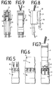
- Die Erfindung ist nachfolgend anhand mehrerer in den Zeichnungen dargestellter Ausführungsformen beschrieben. Es zeigen:
- Fig. 1
- Das Schema eines Teilnehmeranschlusses,
- Fig. 2
- eine Ferntrenneinrichtung mit gesteuerten Siliziumgleichrichtern,
- Fig. 3
- das Verhalten einer Ferntrenneinrichtung mit gesteuerten Siliziumgleichrichtern mit und ohne Koppelglied bei Impulswahl,
- Fig. 4
- eine Ferntrenneinrichtung mit MOS-FET Schaltern,
- Fig. 5
- eine vereinfachte Teilschaltung der Schaltung gemäß Fig. 4,
- Fig. 6
- eine zweite Ausführungsform einer Ferntrenneinrichtung mit MOS-FET Schaltern,
- Fig. 7
- eine dritte Ausführungsform einer Ferntrenneinrichtung mit MOS-FETs und DC/DC-Wandlern.
- Fig. 8
- eine Ferntrenneinrichtung mit gesteuerten Siliziumgleichrichtern und verpolten elektonischen Schaltern und
- Fig. 9
- eine Ferntrenneinrichtung mit MOF-FET Schaltern, deren Schalter gegenseitig verpolt sind.
- Fig. 1 zeigt einen Teilnehmeranschluß, bei dem von einer Vermittlungsstelle 10, die zur Vereinfachung auch die Fernmelde-Entstörstelle beinhaltet, eine Teilnehmerleitung 11 (bestehend aus zwei Leitungen 11a und 11b) zum Übergabepunkt führt, an dem sich eine Ferntrenneinrichtung 12 befindet. Hinter dem Übergabepunkt 12 befindet sich das private Netz 13 mit seinen Endeinrichtungen 14 . Die Ferntrenneinrichtung 12 besteht im wesentlichen aus zwei elektronischen Schaltern 12a, 12b, die ein Abtrennen des Teilnehmers gestatten. Diese Schalter werden durch eine geeignete Ansteuerspannung spannungsabhängig angesteuert. Die Schaltspannung liegt unter der Speisespannung der Teilnehmerleitung 11, so daß die Schalter im normalen Telefonbetrieb geschlossen sind. Im Fehlerfall wird von der Vermittlungsstelle 10 aus eine Messung mit einer Prüfeinrichtung durchgeführt, die mit zwei Spannungen arbeitet. Eine Spannung davon liegt über, während die andere unter der Schaltspannung liegt. Durch eine Spannungsabsenkung unter die Schaltschwelle wird der Schalter geöffnet, und es kann eine Prüfung der Teilnehmerleitung ohne Teilnehmer durchgeführt werden.
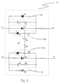
- Fig. 2 zeigt eine bevorzugte Ausführungsform einer Ferntrenneinrichtung, bei der Thyristoren S₁, S₂, welche in die Leitungen A-A' (11a) und B-B' (11b) geschaltet sind, als Schalter verwendet werden. Um die Polungsunabhängigkeit der Ferntrenneinrichtung herzustellen, sind Dioden D3 und D4 parallel zu den Thyristoren S1 und S2 geschaltet, wobei die Durchlaßrichtung der Dioden D3, D4 entgegengesetzt zur Durchlaßrichtung der Thyristoren S1, S2 ist. Entsprechend der Polung der Ferntrenneinrichtung übernimmt in einem Leitungszweig der Thyristor, im anderen die Diode den Stromfluß. Ist z.B. die Ader 11a der Fernmeldeleitung positiv gegenüber der Ader 11b, so fließt der Speisestrom während des Betriebes über den Thyristor S1 und die Diode D4. Möglich ist auch die erfindungsgemäße Ausführung einer Ferntrenneinrichtung mit Triacs. Dabei entfallen die Dioden D3,D4, da ein Triac den Strom in beide Richtungen leitet. Parallel zu den Schaltern sind die Überbrückungswege 20,21 geschaltet. Die spannungsabhängige Einschaltcharakteristik der Thyristoren S1,S2 wird durch die Ansteuerzweige 30,31 erreicht. Um das schnelle Ansprechen der Thyristoren S1,S2 bei Impulswahl zu erreichen, werden beide Ansteuerzweige 30,31 mit einem Koppelglied 40 verbunden.
- Beim Impulswahlverfahren werden im Telefon 14 die Wahlimpulse dadurch erzeugt, daß ein im Telefon befindlicher Wahlimpulsschalter im Takt der Impulse geöffnet und geschlossen wird. Bei geschlossenem Wahlimpulsschalter muß Strom fließen, damit die Wahlimpulse von der Vermittlungsstelle 10 erkannt werden könne. Deshalb muß der entsprechende Thyristor der Ferntrenneinrichtung 12 während eines Wahlimpulses geschlossen sein um einen Stromfluß zu ermöglichen. Beim Öffnen des Wahlimpulsschalters im Telefon wird der Thyristor ebenfalls öffnen, da der Haltestrom unterschritten wird. Ein Schließen des Thyristors muß ca. alle 100 Millisekunden erfolgen. Dies wird beim Fehlen des Koppelgliedes 40 durch den Kondensator im Überbrückungszweig verhindert, weil dieser während des letzten Impulses über den leitenden Thyristor entladen wurde und sich während der Öffnungszeit des Wahlimpulsschalters, die ca. 30-40 Millisekunden beträgt, noch nicht wieder auf die Schaltspannung aufladen konnte. Die Zeitkonstante zum Aufladen des Kondensators C1,C2 im Überbrückungsweg 20,21 liegt, bedingt durch das hochohmige Telefon, zwischen 20 und 100 Sekunden. Die Zeitkonstante des Koppelgliedes 40 ist kleiner 10 Millisekunden, so daß der Kondensator C3 des Koppelgliedes 40 den Zündimpuls für den Thyristor S1,S2 liefern kann, wenn sich der Wahlimpulsschalter im Telefon schließt. Das Koppelglied 40 nutzt damit den nach dem Öffnen des Wahlimpulsschalters entstehenden Ladestrom der Kondensatoren C1,C2 aus, in dem ein Teil dieses Stromes im Kondensator C3 des Koppelgliedes 40 gespeichert wird und als Zündenergie für den Thyristor S1, S2 zur Verfügung steht, wenn der Wahlimpulswahlschalter wieder schließt.
- Fig. 3 zeigt das Verhalten der Ferntrenneinrichtung einmal mit Koppelglied 40 (gestrichelte Linie) und einmal ohne Koppelglied 40 (durchgezogene Linie) bei Impulswahl. Dabei ist das Potential der Ader 11a positiv gegenüber demjenigen der Ader 11b. Fig. 3a zeigt die Zustände des Wahlimpulsschalters im Telefon 14, Fig. 3b zeigt den zeitlichen Verlauf der Ladespannung am Kondensator C1 des Überbrückungsweges 20, Fig. 3c gibt den zeitlichen Verlauf des Schleifenstromes wieder und in Fig. 3d ist der Strom im Koppelglied 40 dargestellt.
- Wird die Schaltung ohne das Koppelglied 40 betrieben, so war der Kondensator C1 vor dem ersten Wahlimpuls 50 auf die Schaltspannung aufgeladen, die durch die Diode D1 bestimmt wird. Der Thyristor S1 kann zünden und es fließt ein konstanter Schleifenstrom 70 während der Impulsdauer. Im Anschluß an den Wahlimpuls 50 lädt sich der Kondensator C1 langsam wieder auf. Die Zeitkonstante ist jedoch sehr hoch, weil der Widerstand des Telefons zwischen den Impulsen 100 K-Ohm bis einige MegaOhm betragen kann. Deshalb hat die Spannung 61 am Kondensator zu Beginn des nächsten Wahlimpulses 51 noch nicht die Schaltspannung erreicht und der Thyristor S1 kann nicht gezündet werden. Während des Impulses 51 fließt ein erhöhter Ladestrom 71, weil das Telefon für die Zeit eines Wahlimpulses niederohmig ( typisch ungefähr 300 Ohm ) wird. Durch den erhöhten Ladestrom steigt die Spannung am Kondensator C1, 62 entsprechend schnell an. Zu Beginn des dritten Impulses 52 hat die Spannung noch nicht die Schaltspannung erreicht, so daß der Thyristor S1 nicht zu Beginn des Impulses, sondern erst zu einem späteren Zeitpunkt 72 gezündet wird. Durch die Entladung des Kondensators C1 entsprechen die Verhältnisse beim vierten Impuls wieder denjenigen beim zweiten Impuls 51.
- Das Verhalten der Schaltung mit einem Koppelglied 40 ist in der Fig. 3 a bis d durchgezogen eingezeichnet. Beim ersten Impuls 50 wird der Thyristor S1 durch die Ladespannung des Kondensators C1 zünden. Beim zweiten Impuls 51 erreicht die Ladespannung nicht für eine Zündung aus. Der Zündimpuls 80 wird deshalb vom Koppelglied 40 geliefert, das sich zwischen den Impulsen aufgeladen hat.
- Fig. 4 zeigt die bevorzugte Ausführungsform der Erfindung bei der die Schalter 12a, 12b durch MOS-FETs gebildet werden. Der MOS-FET Schalter 12a umfaßt die zwei MOS-FET-Zweige 100, 101, während der MOS-FET-Schalter 12b durch die MOS-FET-Zweige 102, 103 gebildet wird. Dabei enthalten die MOS-FET-Zweige 100, 103 p-Kanal-Mos-Fets und die Zweige 101, 102 n-Kanal MOS-FETs. Jeder MOS-FET-Zweig besteht aus einem MOS-FET-Paar (Q1,Q2), (Q3,Q4), (Q6,Q7) und (Q8,Q9), wobei jeweils die Gate- und Source-Anschlüsse eines MOS-FET Paares miteinander verbunden sind. Die Kanal-Substratdioden sind gegeneinander geschaltet, so daß der Strom nur über die Kanäle der MOS-Transistoren zwischen Teilnehmer und Vermittlungsstelle fließen kann. Denkbar ist auch statt der Source- die Drain-Anschlüsse miteinander zu verbinden, um zu verhindern, daß der Strom über die Substrat-Dioden fließen kann. Die p-Kanal Zweige 100,103 übernehmen jeweils den Strom der zum Teilnehmer hinfließt, während die n-Kanal Zweige 101,102 den Strom vom Teilnehmer zur Vermittlungsstelle übernehmen. Da jeder Schalter 12a, 12b sowohl einen n- als auch ein p-Kanal Zweig enthält, arbeitet die Schaltung polungsunabhängig.
- Die Ansteuerung der MOS-FET-Zweige 100,101,102 und 103 erfolgt über je einen Spannungsteiler (Rt1,Rt8), (Rt2,Rt7), (Rt3,Rt6) und (Rt4,Rt5). Der Widerstand Rt8 des Spannungsteilers des Zweiges 100 kann durch einen MOS-FET Q5 mit einem seriellen Widerstand Rs1 und einer Diode Ds1 überbrückt werden. Das Gate des Ansteuerungs-MOS-FETs Q5 wird durch den Spannungsteiler Rs2, Rs3 angesteuert. Dasselbe gilt für den Zweig 103, hier überbrückt ein Ansteuerungs-MOS-FET Q10 mit einem seriellen Widerstand Rs4 und einer Diode Ds2 dem Widerstand Rt5 im durchgeschalteten Zustand des MOS-FETs. Das Gate von Q10 ist mit einem Spannungsteiler, gebildet aus den Widerständen Rs5 und Rs6 beschaltet. Zur Spannungsbegrenzung sind zwischen den Source und den Basis-Leitungen der jeweiligen Zweige 100, 101, 102 und 103 Zenerdioden-Paare Z1, Z2, Z4 und Z5 geschaltet. Dasselbe gilt für die MOS-FETs Q5 und Q10, dort sind es die Zenerdioden-Paare Z6 und Z3. Die Beschaltung und die Spannungsteiler sind so dimensioniert, daß sich eine hohe Einschaltspannung und eine niedrige Ausschaltspannung ergibt. Die Einschaltspannung kann einige Volt unter der Speisespannung des Fernmeldenetzes liegen, während die Ausschaltspannung unter 10 Volt liegen kann. Dieses Schaltverhalten trägt der Tatsache Rechnung, daß bei der Inbetriebnahme eines niederohmigen Endgerätes die Spannung deutlich unter die Einschaltschwelle der Ferntrenneinrichtung absinkt. Die Ansteuerungs-MOS-FETs Q5 und Q10 erzeugen ein Hysterese-Verhalten der Schaltschwelle für die n-Kanal Zweige 101 und 102. Die Kondensatoren CG1 bis CG4, welche zwischen die Source- und Gate-Leitungen der Zweige 100, 101, 102 und 103 geschaltet sind, bewirken ein verzögertes Ausschalten der MOS-FETs und ermöglichen so die Übertragung von Rufwechselströmen.
- Fig. 5 zeigt eine vereinfachte Teilschaltung der Schaltung nach Fig. 4 und die zugehörige Beschaltung auf der Amt- und der Teilnehmerseite. Anhand Fig. 5 wird die Wirkungsweise der Schaltung gemäß Fig. 4 erklärt. Das Amt besteht, vereinfacht dargestellt, aus einer Gleichspannungsquelle Vamt und zwei Widerständen Ra und Rb, welche die Speise- und Leitung-Widerstände für jede Ader 11a und 11b darstellen. Das Telefon auf der Teilnehmerseite besteht in dieser Vereinfachung aus einem Gabelumschalter GU und einen Widerstand Rtel. Ist der Gabelumschalter GU geöffnet, d.h. der Hörer ist aufgelegt, so steht beim Teilnehmer und damit am Eingang der Ferntrenneinrichtung die volle Speisespannung Vamt zur Verfügung, da die Widerstände Ra und Rb klein gegenüber dem Isolationswiderstand des Telefons 14 sind. Bei geschlossenem Gabelumschalter GU ist das Telefon 14 niederohmig und die Widerstände Ra, Rb und Rtel bilden einen Spannungsteiler, wobei am Telefon 14, je nach Leitungslänge, nur noch 15 bis 30% der Amtsspannung Vamt ansteht. Die Schaltschwelle der Ferntrenneinrichtung darf daher nicht höher als diese Grenze sein und würde bei einer Amtsspannung Vamt von 60V ca. 9V betragen. Es ist jedoch erwünscht im Testfall Messungen mit Spannungen zwische 10 und 20 V durchzuführen, ohne daß der Teilnehmer zugeschaltet wird. Dies ist bei einer einfachen Schaltschwelle von 9V nicht möglich. Es wird daher eine Ansteuerschaltung benötigt, die eine hohe Einschaltschwelle und eine niedrige Ausschaltschwelle hat, d.h. ein Hystereseverhalten aufweist. Die beiden MOS-FETs Q1 und Q2, welche in die Teilnehmerleitung 11a seriell eingeschaltet sind, wobei die jeweiligen Source- und Gate-Anschlüsse miteinander verbunden sind, leiten im eingeschalteten Zustand den Strom zum Telefon 14. Die Ansteuerung des Zweiges 100, gebildet aus Q1 und Q2, erfolgt durch den Spannungsteiler Rt1 und Rt8. Durch diese beiden Widerstände wird die Einschaltschwelle der Schaltung festgelegt und kann beispielsweise bei 50% der Amtsspannung (Speisespannung) liegen. Damit ist die Einschaltschwelle wesentlich größer als die Spannung, die bei geschlossenem Gabelschalter GU noch am Eingang der Ferntrenneinrichtung zur Verfügung stünde. Wird die Einschaltschwelle überschritten, so werden die MOS-FETs Q1 und Q2 leitend und es steht am Ausgang der Ferntrenneinrichtung, also am Spannungsteiler Rs2, Rs3, die gleiche Spannung wie am Eingang derselben an. Der Spannungsteiler Rs2, Rs3 ist so dimensioniert, daß bei kleinen Spannungen von ca 15 bis 20% der Amtsspannung der n-Kanal MOS-FET Q5 leitend ist. Dadurch wird der hochohmige Widerstand Rt8 durch den niederohmige Widerstand Rs1 überbrückt. Die Folge ist, daß, selbst wenn der Gabelumschalter GU geschlossen ist, die MOS-FETs Q1 und Q2 auch bei kleinen Spannungen leitend bleiben. Da sich die MOS-FETs praktisch leistungslos steuern lassen, können die Spannungsteilerwiderstände sehr hochohmig, d.h. im MegaOhm Bereich gehalten werden, so daß die Eigenstromaufnahme sehr klein ist.
- Fig. 6 zeigt eine vereinfachte Ausführungsform der Erfindung, bei der in den Zweigen 100, 101, 102 und 103 statt eines MOS-FET Paares nur jeweils ein einzelner MOS-FET verwendet wird. Die Schalter 12a und 12b bestehen aus je einem n-(Q1,Q8) und einem p-Kanal (Q3,Q6) MOS-FET, die so parallel geschaltet werden, daß die Anoden der Substrat-Dioden zum Teilnehmer hin geschaltet sind. In diesem Fall können die Substratdioden der MOT-FETs nur Strom vom Teilnehmer zur Vermittlungsstelle leiten. Deshalb ist die Schaltschwelle für den Rückflußzweig nicht größer als 0,6V. Ansonsten entspricht der Schaltungaufbau der Ausführungsform gemäß Fig.4.
- Fig. 7 zeigt eine weitere bevorzugte Ausführungsform der Erindung, wobei die Steuerung der Zweige schematisch dargestellt ist und derjenigen der Ausführungsform gemäß Fig.4 entsprichen. Die n-Kanal MOS-FET Zweige 101 und 102 der Schaltung gemäß Fig. 4 können eingespart werden, wenn die p-Kanal Zweige 100 und 103 zusätzlich zu den oben beschriebenen Ansteuerschaltungen 160,161, die das Hysterese-Verhalten erzeugen, mit jeweils einem DC/DC-Wandler 150,151 angesteuert werden. Der Wandler 150, 160 erzeugt eine negative Spannung, wenn das entsprechende p-Kanal Paar 100, 103 im negativen Zweig der Fernmeldeleitung liegt und Strom von der Endeinrichtung zur Vermittlungsstelle führt. Eine komplementäre Schaltung mit n-Kanal-Schaltern und DC/DC-Wandlern, die ein positives Potential für den n-Kanal-Schalter erzeugen, der im positiven Zweig liegt, ist ebenfalls denkbar.
- Fig. 8 zeigt eine Ferntrenneinrichtung mit gesteuerten Siliziumgleichrichtern und stellt eine modifizierte Schaltung aus Fig. 2 dar. Der elektronische Schalter 12b in der Ader b ist gegenüber dem Schalter 12a verpolt. Somit ist die Durchlaßrichtung der Dioden D2, D4 und des Thyristors S2 antiparallel gegenüber derjenigen der Dioden D1, D3 und des Thyristors S1 in der Ader a. Bei positiver Spannung der Ader a gegenüber der Ader b sperren die Thyristoren S1 und S2, wenn die Meßspannung unter der Schaltschpannung liegt.Bei negativer Meßspannung werden die Dioden D3 und D4 leitend und die Teilnehmerseite wird in die Messungen mit einbezogen, d.h. die Schalter 12a und 12b werden wieder eingeschaltet.
- Fig. 9 zeigt die entsprechend modifizierte MOS-FET-Schaltung aus Fig. 6. Dabei sind die MOS-FET-Transistoren in der Ader b vertauscht. Der Transistor Q6 ist nunmehr vom n-Kanal-Typ und der Transistor Q8 vom p-Kanal-Typ. In der Schaltung gemäß Fig. 6 sind die Schalter 12a und 12b demgegenüber symmetrisch. Zusätzlich ist noch der zugehörige Schmitt-Trigger-Transistor Q10 der entsprechenden Ansteuerung gegen den komplementären p-Kanal-Typ ausgetauscht.
-
- 10
- Vermittlungsstelle
- 11
- Teilnehmerleitung
- 11a
- Teilnehmerleitung a
- 11b
- Teilnehmerleitung b
- 12
- Ferntrenneinrichtung
- 12a
- elektronischer Schalter
- 12b
- elektronischer Schalter
- 13
- privates Netz
- 14
- Endeinrichtung
- 20
- Überbrückungsweg
- 21
- Überbrückungsweg
- 30
- Ansteuerung
- 31
- Ansteuerung
- 40
- Koppelglied
- D1-D4
- Diode
- C1-C2
- Kapazität
- R1
- Widerstand
- R2-R4
- Widerstand
- S1-S2
- Siliziumgleichrichter
- 50-53
- Wahlimpuls
- 60-62
- Kondensatorspannung
- 70-73
- Ladestrom
- 80-81
- Zündimpuls
- 100
- Schalter-Zweig
- 101
- Schalter-Zweig
- 102
- Schalter-Zweig
- 103
- Schalter-Zweig
- Cg1-Cg4
- Kapazität
- Ds1-Ds2
- Diode
- Q1-Q10
- MOS-FET
- Rt1-Rt8
- Widerstand
- Rs1-Rs6
- Widerstand
- Z1-Z6
- Zenerdiodenpaar
- Ra
- Leitungswiderstand
- Rb
- Leitundswiderstand
- GU
- Gabelumschalter
- Rtel
- Telefonwiderstand
- Vamt
- Amtsspannung
- 150
- Steuerung
- 151
- Steuerung
- 160
- DC/DC-Wandler
- 161
- DC/DC-Wandler
- SZ
- Schaltzustandsachse
- Um
- Meßspannung
- Us
- Einschaltspannung
- an
- Schaltzustand
- aus
- Schaltzustand
- Ud
- Diodenspannungsabfall
Claims (22)
- Ferntrenneinrichtung aus zwei elektronischen, in die jeweilige Teilnehmerleitung (11a, 11b) geschalteten Schaltern (12a,12b), wobei jeder Schalter (12a,12b) einen gesteuerten Siliziumgleichrichter (S1,S2) enthält, dessen Steuereingang durch eine parallel geschaltete Zenerdiode (D1, D2) mit Widerstand (R1,R2) angesteuert wird und eine parallele Überbrückung (20,21) des Siliziumgleichrichters (S1,S2) enthält, welche aus einer Kapazität (C1,C2) und einem Widerstand (R3,R4) besteht,
dadurch gekennzeichnet,
daß die Steuereingänge der Siliziumgleichrichter (S1,S2) mittels eines Koppelgliedes (40) verbunden sind. - Ferntrenneinrichtung nach Anspruch 1, dadurch gekennzeichnet, daß das Koppelglied (40) aus der Serienschaltung einer Kapazität (C3) und eines Widerstandes (R5) besteht.
- Ferntrenneinrichtung nach Anspruch 2, dadurch gekennzeichnet, daß die elektronischen Schalter (12a, 12b) mit entgegengesetzter Polung in die Leitungen (11a, 11b) eingesetzt sind.
- Ferntrenneinrichtung aus zwei elektronischen, in die jeweilige Teilnehmerleitung (11a,11b) geschalteten Schaltern (12a,12b), wobei jeder Schalter (12a,12b) mindestens einen MOS-FET enthält,
dadurch gekennzeichnet,
daß selbstsperrende MOS-FETs vom Anreicherungstyp verwendet werden. - Ferntrenneinrichtung nach Anspruch 4, dadurch gekennzeichnet, daß die MOS-FET Schalter (12a,12b) so angesteuert werden, daß sie eine hohe Einschaltschwelle und eine niedrige Ausschaltschwelle aufweisen.
- Ferntrenneinrichtung nach Anspruch 5, dadurch gekennzeichnet, daß die Ansteuerung eines MOS-FET Schalters (12a,12b) aus mindestens einem Spannungsteiler ((Rt1,Rt8), (Rt2,Rt7), (Rt3,Rt6), (Rt4,Rt5) und einem Ansteuerungs-MOS-Fet (Q5,Q10) besteht.
- Ferntrenneinrichtung nach Anspruch 6, dadurch gekennzeichnet, daß beide Ansteuerungs-MOS-FETs vom gleichen Typ sind.
- Ferntrenneinrichtung nach Anspruch 7, dadurch gekennzeichnet, daß beide Ansteurungs-MOS-FETs vom n-Kanal-Typ sind.
- Ferntrenneinrichtung nach einem der Ansprüche 6 bis 8, dadurch gekennzeichnet, daß die Einschaltspannung in der Größenordnung der Speisespannung des Fernmeldenetzes liegt.
- Ferntrenneinrichtung nach Anspruch 9, dadurch gekennzeichnet, daß die Ausschaltspannung ca. 15% der Speisespannung des Fernmeldenetzes beträgt.
- Ferntrenneinrichtung nach einem oder mehreren der Ansprüche 5 bis 10, dadurch gekennzeichnet, daß ein MOS-FET Schalter (12a,12b) aus einem n-Kanal (101,102) und einem dazu parallel geschalteten p-Kanal MOS-FET Zweig (100,103) besteht.
- Ferntrenneinrichtung nach Anspruch 11, dadurch gekennzeichnet, daß zwischen der gemeinsamen Sourceleitung und der Gate-Leitung eines MOS-FET Zweiges (100,101,102,103) Kondensatoren (Cg1,Cg2,Cg3,Cg4) geschaltet sind.
- Ferntrenneinrichtung nach Anspruch 12, dadurch gekennzeichnet, daß ein MOS-FET Zweig (100,101,102,103) aus einem MOS-FET (Q1,Q3,Q6,Q8) besteht.
- Ferntrenneinrichtung nach Anspruch 13, dadurch gekennzeichnet, daß die Anoden der Substrat-Dioden zum Teilnehmer hin geschaltet sind.
- Ferntrenneinrichtung nach Anspruch 11 oder 12, dadurch gekennzeichnet, daß ein MOS-FET Zweig (100,101,102,103) ein Paar MOS-FETs ((Q1,Q2), (Q3,Q4), (Q6,Q7), (Q8,Q9)) enthält.
- Ferntrenneinrichtung nach Anspruch 15, dadurch gekennzeichnet, daß die Kanalsubstratdioden eines MOS-FET Paares ((Q1,Q2), Q3,Q4), Q6,Q7), Q8,Q9)) gegeneinander geschaltet sind.
- Ferntrenneinrichtung nach Anspruch 16, dadurch gekennzeichnet, daß jeweils die Gate- und die Source-Anschlüsse eines MOS-FET Paares ((Q1,Q2), Q3,Q4), Q6,Q7), Q8,Q9)) miteinander verbunden sind.
- Ferntrenneinrichtung nach einem oder mehreren der Ansprüche 5 bis 10, dadurch gekennzeichnet, daß ein MOS-FET Schalter (12a,12b) aus einem p-Kanal Zweig (100,103) besteht, wobei der Zweig ein Paar MOS-FETs ((Q1,Q2), Q8,Q9) enthält, deren jeweilige Gate- und Source-Anschlüsse miteinander verbunden sind.
- Ferntrenneinrichtung nach Anspruch 18, dadurch gekennzeichnet, daß die Gate-Leitung jedes Zweiges (100,103) zusätzlich durch einen DC/DC-Wandler (150,151) angesteuert wird.
- Ferntrenneinrichtung nach Anspruch 5, dadurch gekennzeichnet, daß die Einschaltschwelle für negative Spannungen verschieden von derjenigen für positive Spannungen ist.
- Ferntrenneinrichtung nach Anspruch 20 und einem oder mehreren der Ansprüche 6 und 9 bis 17, dadurch gekennzeichnet, daß einer der beiden Ansteuerungs-MOS-FETs (Q5,Q10) ein p-Kanal-Typ und der andere ein n-Kanal-Typ ist, und daß die MOS-FET-Transistoren (Q1,Q3; Q6,Q8) in einer Ader vertauscht sind.
- Ferntrenneinrichtung nach einem oder mehreren der vorangegangenen Ansprüche, dadurch gekennzeichnet, daß die Schaltung komplementär aufgebaut ist.
Applications Claiming Priority (2)
| Application Number | Priority Date | Filing Date | Title |
|---|---|---|---|
| DE4127896 | 1991-08-22 | ||
| DE4127896A DE4127896C2 (de) | 1991-08-22 | 1991-08-22 | Anschlußleiste für die Fernmelde- und Datentechnik |
Publications (3)
| Publication Number | Publication Date |
|---|---|
| EP0529267A2 true EP0529267A2 (de) | 1993-03-03 |
| EP0529267A3 EP0529267A3 (en) | 1994-03-23 |
| EP0529267B1 EP0529267B1 (de) | 1999-06-16 |
Family
ID=6438911
Family Applications (1)
| Application Number | Title | Priority Date | Filing Date |
|---|---|---|---|
| EP92111854A Expired - Lifetime EP0529267B1 (de) | 1991-08-22 | 1992-09-09 | Anschlussleiste für die Fernmelde- und Datentechnik |
Country Status (15)
| Country | Link |
|---|---|
| US (1) | US5297975A (de) |
| EP (1) | EP0529267B1 (de) |
| AT (1) | ATE181476T1 (de) |
| AU (1) | AU659849B2 (de) |
| BR (1) | BR9203287A (de) |
| DE (2) | DE4127896C2 (de) |
| DK (1) | DK0529267T3 (de) |
| ES (2) | ES2134203T3 (de) |
| GR (1) | GR3031205T3 (de) |
| IE (1) | IE922448A1 (de) |
| MX (1) | MX9204826A (de) |
| NO (1) | NO307589B1 (de) |
| RU (1) | RU2077096C1 (de) |
| TR (1) | TR26715A (de) |
| UA (1) | UA25891C2 (de) |
Cited By (1)
| Publication number | Priority date | Publication date | Assignee | Title |
|---|---|---|---|---|
| EP0690523A1 (de) * | 1994-07-01 | 1996-01-03 | Minnesota Mining And Manufacturing Company | Querverbindungssystem für Telekommunikationssysteme |
Families Citing this family (9)
| Publication number | Priority date | Publication date | Assignee | Title |
|---|---|---|---|---|
| DE4325952C2 (de) * | 1993-07-27 | 1997-02-13 | Krone Ag | Anschlußleiste für hohe Übertragungsraten in der Telekommunikations- und Datentechnik |
| DE4333263C2 (de) * | 1993-09-24 | 1995-09-28 | Krone Ag | Reihenklemme |
| FR2746552B1 (fr) * | 1996-03-22 | 1998-05-07 | Pouyet Sa | Procede et dispositif de connexion securisee d'un cordon de brassage sur une reglette d'interconnexion de lignes telephoniques ou informatiques |
| FR2810165B1 (fr) * | 2000-06-09 | 2006-10-06 | Entrelec Sa | Dispositif de connexion autodenudante pour un conducteur electrique gaine |
| DK1444754T3 (en) * | 2001-11-14 | 2017-07-10 | Commscope Connectivity Spain Sl | Multiple terminal block and method of sealing this |
| DE10313358B3 (de) * | 2003-03-25 | 2004-08-05 | Siemens Ag | Patchpanel zur Montage an einer Wand oder in einem Baugruppenträger |
| AU2007278522B2 (en) | 2006-07-25 | 2011-07-28 | Adc Gmbh | Connector block |
| DK2044654T3 (da) | 2006-07-25 | 2010-04-19 | Adc Gmbh | Forbindelsesblok |
| AU313574S (en) | 2006-07-25 | 2007-04-10 | Tyco Electronics Services Gmbh | Connector block |
Family Cites Families (14)
| Publication number | Priority date | Publication date | Assignee | Title |
|---|---|---|---|---|
| DE2147336A1 (de) * | 1971-09-22 | 1973-03-29 | Siemens Ag | Verteilergestell fuer fernmelde-, insbesondere fernsprechanlagen |
| SE377636B (de) * | 1973-11-12 | 1975-07-14 | Asea Ab | |
| US4008941A (en) * | 1976-03-04 | 1977-02-22 | Amp Incorporated | Printed circuit board housing system |
| FR2420273A1 (fr) * | 1978-03-17 | 1979-10-12 | Alsthom Cgee | Bloc de jonction a carte de circuit imprime |
| GB2061030A (en) * | 1979-10-15 | 1981-05-07 | Bunker Ramo | Apparatus for interconnection of a multi-channel communication network |
| DE3311476A1 (de) * | 1983-03-29 | 1984-10-04 | Siemens AG, 1000 Berlin und 8000 München | Verteilerliste mit einer mehrzahl von dem abisolierfreien anschluss elektrischer leiter gestattenden anschlussklammen |
| EP0152743A1 (de) * | 1984-01-27 | 1985-08-28 | Litton Precision Products International GmbH | Modularer elekrischer Steckverbinder |
| DE3415369A1 (de) * | 1984-04-25 | 1985-11-07 | Krone Gmbh, 1000 Berlin | Anschlussleiste mit lsa-plus-anschlusselementen zum anschluss von kabeladern und freiluftkabel (dropwire-kabel) |
| DE3614592C1 (de) * | 1986-04-30 | 1987-07-23 | Krone Ag | Anschlussleiste fuer Kabeladern,insbesondere von Fernsprechkabeln |
| DE3644349C1 (de) * | 1986-12-19 | 1988-02-25 | Krone Ag | Anschlussleiste fuer die Fernmeldetechnik |
| DE3710896A1 (de) * | 1987-04-01 | 1988-10-20 | Krone Ag | Verteilerleiste fuer fernmeldekabel, insbesondere hauseingangsverteilerleiste |
| DE3927573C1 (de) * | 1989-08-21 | 1990-06-07 | Siemens Ag, 1000 Berlin Und 8000 Muenchen, De | |
| EP0446572B1 (de) * | 1990-03-13 | 1995-01-11 | KRONE Aktiengesellschaft | Anschlussleiste für die Fernmelde- und Datentechnik |
| US5145404A (en) * | 1990-10-01 | 1992-09-08 | United Technologies Automotive, Inc. | Switch terminal board cover with electrical lead isolation |
-
1991
- 1991-08-22 DE DE4127896A patent/DE4127896C2/de not_active Expired - Fee Related
-
1992
- 1992-07-27 IE IE244892A patent/IE922448A1/en unknown
- 1992-07-28 AU AU20604/92A patent/AU659849B2/en not_active Ceased
- 1992-08-07 ES ES92113511T patent/ES2134203T3/es not_active Expired - Lifetime
- 1992-08-14 NO NO923183A patent/NO307589B1/no not_active IP Right Cessation
- 1992-08-19 TR TR92/0749A patent/TR26715A/xx unknown
- 1992-08-20 MX MX9204826A patent/MX9204826A/es not_active IP Right Cessation
- 1992-08-21 BR BR929203287A patent/BR9203287A/pt not_active IP Right Cessation
- 1992-08-21 RU SU925052395A patent/RU2077096C1/ru active
- 1992-08-24 US US07/934,862 patent/US5297975A/en not_active Expired - Fee Related
- 1992-09-09 ES ES92111854T patent/ES2134202T3/es not_active Expired - Lifetime
- 1992-09-09 EP EP92111854A patent/EP0529267B1/de not_active Expired - Lifetime
- 1992-09-09 AT AT92111854T patent/ATE181476T1/de active
- 1992-09-09 DE DE59209713T patent/DE59209713D1/de not_active Expired - Fee Related
- 1992-09-09 DK DK92111854T patent/DK0529267T3/da active
-
1993
- 1993-06-18 UA UA93003003A patent/UA25891C2/uk unknown
-
1999
- 1999-09-15 GR GR990402299T patent/GR3031205T3/el unknown
Cited By (1)
| Publication number | Priority date | Publication date | Assignee | Title |
|---|---|---|---|---|
| EP0690523A1 (de) * | 1994-07-01 | 1996-01-03 | Minnesota Mining And Manufacturing Company | Querverbindungssystem für Telekommunikationssysteme |
Also Published As
| Publication number | Publication date |
|---|---|
| DE59209713D1 (de) | 1999-07-22 |
| ES2134202T3 (es) | 1999-10-01 |
| NO307589B1 (no) | 2000-04-25 |
| GR3031205T3 (en) | 1999-12-31 |
| DE4127896A1 (de) | 1993-02-25 |
| ATE181476T1 (de) | 1999-07-15 |
| IE922448A1 (en) | 1993-02-24 |
| US5297975A (en) | 1994-03-29 |
| AU659849B2 (en) | 1995-06-01 |
| BR9203287A (pt) | 1993-04-06 |
| ES2134203T3 (es) | 1999-10-01 |
| EP0529267A3 (en) | 1994-03-23 |
| NO923183D0 (no) | 1992-08-14 |
| NO923183L (no) | 1993-02-23 |
| DE4127896C2 (de) | 1996-10-24 |
| TR26715A (tr) | 1995-05-15 |
| RU2077096C1 (ru) | 1997-04-10 |
| MX9204826A (es) | 1994-08-31 |
| UA25891C2 (uk) | 1999-02-26 |
| AU2060492A (en) | 1993-02-25 |
| EP0529267B1 (de) | 1999-06-16 |
| DK0529267T3 (da) | 1999-11-22 |
| HK1004738A1 (en) | 1998-12-04 |
Similar Documents
| Publication | Publication Date | Title |
|---|---|---|
| EP0026411B1 (de) | Schaltungsanordnung zur Feststellung des Schaltzustandes einer Teilnehmeranschlussleitung in Fernsprechvermittlungsanlagen | |
| EP0529267A2 (de) | Anschlussleiste für die Fernmelde- und Datentechnik | |
| DE4200775C1 (de) | ||
| DE2922271C2 (de) | Schaltungsanordnung zum Speisen von Signalübertragungsleitungen in Fernmeldeanlagen | |
| DE925778C (de) | Anordnung fuer Fernsprechanlagen mit Waehlerbetrieb | |
| DE3633561C1 (en) | Change-over switching device for a telephone facility for connecting a number of extensions to a common telephone line | |
| DE2256997A1 (de) | Fernsprechteilnehmerschaltung | |
| DE1288166B (de) | Doppeltgerichteter Verstaerker fuer die Signaluebertragung ueber Teilnehmeranschlussleitungen | |
| DE3618500A1 (de) | Schaltungsanordnung zum verpolschutz | |
| DE69520941T2 (de) | Schaltvorrichtung für telekommunikationskanal | |
| DE2749458A1 (de) | Vorrichtung zum unterdruecken unerwuenschter klingeltoene an fernsprechgeraeten | |
| EP0014328A1 (de) | Belegschaltung an einer "ankommenden" c-Ader in einer Fernmeldeeinrichtung | |
| DE2200341C3 (de) | Schaltungsanordnung zum Prüfen der Teilnehmeranschlußleitungen in Fernmelde-, insbesondere Fernsprechanlagen mit jeweils zwei über eine gemeinsame Anschlußleitung angeschlossenen Teilnehmerstellen | |
| DE2931529A1 (de) | Teilnehmerseitiges datenuebertragungsgeraet, insbesondere fuer bildschirmtextbetrieb | |
| DE944800C (de) | Schaltungsanordnung fuer Fernmelde-, insbesondere Fernsprechanlagen | |
| DE2302024C3 (de) | Schaltungsanordnung zum Anschließen von Telegrafie- und Datenteilnehmern an eine Vermittlungsanlage | |
| DE2938970C2 (de) | Schaltungsanordnung zur Verhinderung der nachteiligen Auswirkung von Wechselspannungsanteilen bei der Erkennung des Schaltzustandes von Teilnehmeranschlußleitungen in Fernsprechvermittlungsanlagen | |
| CH564291A5 (de) | ||
| DE3937181A1 (de) | Wechselschaltvorrichtung fuer eine fernsprecheinrichtung zum anschluss zweier sprechstellen an eine gemeinsame fernsprechleitung | |
| DE3128635C2 (de) | Schaltungsanordnung zum Aussenden von Datensignalen | |
| DE2207255C3 (de) | Schaltungsanordnung zum Übertragen von elektrischer Energie in zentralgespeisten Fernmeldeanlagen | |
| DE696282C (de) | Schaltungsanordnung fuer Fernmeldeanlagen, insbesondere Fernsprechanlagen, mit Gesellschaftsleitungen | |
| DE3641763A1 (de) | Wechselschaltvorrichtung fuer eine fernsprecheinrichtung zum anschluss mehrerer sprechstellen an eine gemeinsame fernsprechleitung | |
| DE2044886C (de) | Schaltungsanordnung zur Ermittlung rufender Teilnehmerstellen in Fernmelde-, insbesondere Fernsprechanlagen mit Vorfeldeinrichtungen ohne eigene Stromversorgung | |
| DE1263859B (de) | Schaltungsanordnung zum impulsmaessigen UEbertragen von elektrischer Energie in elektrischen Anlagen, insbesondere in Zeitmultiplex-Fernsprechvermittlungssystemen |
Legal Events
| Date | Code | Title | Description |
|---|---|---|---|
| PUAI | Public reference made under article 153(3) epc to a published international application that has entered the european phase |
Free format text: ORIGINAL CODE: 0009012 |
|
| AK | Designated contracting states |
Kind code of ref document: A2 Designated state(s): AT BE CH DE DK ES FR GB GR IT LI LU MC NL PT SE |
|
| 17P | Request for examination filed |
Effective date: 19930126 |
|
| PUAL | Search report despatched |
Free format text: ORIGINAL CODE: 0009013 |
|
| AK | Designated contracting states |
Kind code of ref document: A3 Designated state(s): AT BE CH DE DK ES FR GB GR IT LI LU MC NL PT SE |
|
| 17Q | First examination report despatched |
Effective date: 19940715 |
|
| R17P | Request for examination filed (corrected) |
Effective date: 19930126 |
|
| RAP1 | Party data changed (applicant data changed or rights of an application transferred) |
Owner name: KRONE AKTIENGESELLSCHAFT |
|
| GRAG | Despatch of communication of intention to grant |
Free format text: ORIGINAL CODE: EPIDOS AGRA |
|
| GRAH | Despatch of communication of intention to grant a patent |
Free format text: ORIGINAL CODE: EPIDOS IGRA |
|
| GRAH | Despatch of communication of intention to grant a patent |
Free format text: ORIGINAL CODE: EPIDOS IGRA |
|
| GRAA | (expected) grant |
Free format text: ORIGINAL CODE: 0009210 |
|
| AK | Designated contracting states |
Kind code of ref document: B1 Designated state(s): AT BE CH DE DK ES FR GB GR IT LI LU MC NL PT SE |
|
| REF | Corresponds to: |
Ref document number: 181476 Country of ref document: AT Date of ref document: 19990715 Kind code of ref document: T |
|
| REG | Reference to a national code |
Ref country code: CH Ref legal event code: NV Representative=s name: MICHELI & CIE INGENIEURS-CONSEILS Ref country code: CH Ref legal event code: EP |
|
| ET | Fr: translation filed | ||
| REF | Corresponds to: |
Ref document number: 59209713 Country of ref document: DE Date of ref document: 19990722 |
|
| GBT | Gb: translation of ep patent filed (gb section 77(6)(a)/1977) |
Effective date: 19990707 |
|
| REG | Reference to a national code |
Ref country code: PT Ref legal event code: SC4A Free format text: AVAILABILITY OF NATIONAL TRANSLATION Effective date: 19990625 |
|
| REG | Reference to a national code |
Ref country code: ES Ref legal event code: FG2A Ref document number: 2134202 Country of ref document: ES Kind code of ref document: T3 |
|
| PGFP | Annual fee paid to national office [announced via postgrant information from national office to epo] |
Ref country code: DE Payment date: 19991022 Year of fee payment: 8 |
|
| REG | Reference to a national code |
Ref country code: DK Ref legal event code: T3 |
|
| RAP2 | Party data changed (patent owner data changed or rights of a patent transferred) |
Owner name: KRONE GMBH |
|
| PLBE | No opposition filed within time limit |
Free format text: ORIGINAL CODE: 0009261 |
|
| STAA | Information on the status of an ep patent application or granted ep patent |
Free format text: STATUS: NO OPPOSITION FILED WITHIN TIME LIMIT |
|
| 26N | No opposition filed | ||
| REG | Reference to a national code |
Ref country code: CH Ref legal event code: PFA Free format text: KRONE AKTIENGESELLSCHAFT TRANSFER- KRONE GMBH |
|
| NLT2 | Nl: modifications (of names), taken from the european patent patent bulletin |
Owner name: KRONE GMBH |
|
| REG | Reference to a national code |
Ref country code: FR Ref legal event code: CJ |
|
| PGFP | Annual fee paid to national office [announced via postgrant information from national office to epo] |
Ref country code: GB Payment date: 20000825 Year of fee payment: 9 |
|
| PGFP | Annual fee paid to national office [announced via postgrant information from national office to epo] |
Ref country code: PT Payment date: 20000831 Year of fee payment: 9 |
|
| PGFP | Annual fee paid to national office [announced via postgrant information from national office to epo] |
Ref country code: ES Payment date: 20000912 Year of fee payment: 9 |
|
| PGFP | Annual fee paid to national office [announced via postgrant information from national office to epo] |
Ref country code: FR Payment date: 20000921 Year of fee payment: 9 |
|
| PGFP | Annual fee paid to national office [announced via postgrant information from national office to epo] |
Ref country code: MC Payment date: 20000925 Year of fee payment: 9 Ref country code: DK Payment date: 20000925 Year of fee payment: 9 Ref country code: AT Payment date: 20000925 Year of fee payment: 9 |
|
| PGFP | Annual fee paid to national office [announced via postgrant information from national office to epo] |
Ref country code: SE Payment date: 20000926 Year of fee payment: 9 Ref country code: NL Payment date: 20000926 Year of fee payment: 9 Ref country code: BE Payment date: 20000926 Year of fee payment: 9 |
|
| PGFP | Annual fee paid to national office [announced via postgrant information from national office to epo] |
Ref country code: LU Payment date: 20000927 Year of fee payment: 9 Ref country code: CH Payment date: 20000927 Year of fee payment: 9 |
|
| PGFP | Annual fee paid to national office [announced via postgrant information from national office to epo] |
Ref country code: GR Payment date: 20000928 Year of fee payment: 9 |
|
| REG | Reference to a national code |
Ref country code: PT Ref legal event code: PD4A Free format text: KRONE GMBH DE Effective date: 20000616 |
|
| PG25 | Lapsed in a contracting state [announced via postgrant information from national office to epo] |
Ref country code: DE Free format text: LAPSE BECAUSE OF NON-PAYMENT OF DUE FEES Effective date: 20010601 |
|
| NLS | Nl: assignments of ep-patents |
Owner name: KRONE GMBH |
|
| PG25 | Lapsed in a contracting state [announced via postgrant information from national office to epo] |
Ref country code: MC Free format text: LAPSE BECAUSE OF NON-PAYMENT OF DUE FEES Effective date: 20010909 Ref country code: LU Free format text: LAPSE BECAUSE OF NON-PAYMENT OF DUE FEES Effective date: 20010909 Ref country code: GB Free format text: LAPSE BECAUSE OF NON-PAYMENT OF DUE FEES Effective date: 20010909 Ref country code: DK Free format text: LAPSE BECAUSE OF NON-PAYMENT OF DUE FEES Effective date: 20010909 Ref country code: AT Free format text: LAPSE BECAUSE OF NON-PAYMENT OF DUE FEES Effective date: 20010909 |
|
| PG25 | Lapsed in a contracting state [announced via postgrant information from national office to epo] |
Ref country code: SE Free format text: LAPSE BECAUSE OF NON-PAYMENT OF DUE FEES Effective date: 20010910 Ref country code: ES Free format text: LAPSE BECAUSE OF NON-PAYMENT OF DUE FEES Effective date: 20010910 |
|
| PG25 | Lapsed in a contracting state [announced via postgrant information from national office to epo] |
Ref country code: LI Free format text: LAPSE BECAUSE OF NON-PAYMENT OF DUE FEES Effective date: 20010930 Ref country code: GR Free format text: LAPSE BECAUSE OF NON-PAYMENT OF DUE FEES Effective date: 20010930 Ref country code: CH Free format text: LAPSE BECAUSE OF NON-PAYMENT OF DUE FEES Effective date: 20010930 Ref country code: BE Free format text: LAPSE BECAUSE OF NON-PAYMENT OF DUE FEES Effective date: 20010930 |
|
| PG25 | Lapsed in a contracting state [announced via postgrant information from national office to epo] |
Ref country code: PT Free format text: LAPSE BECAUSE OF NON-PAYMENT OF DUE FEES Effective date: 20020131 |
|
| BERE | Be: lapsed |
Owner name: KRONE G.M.B.H. Effective date: 20010930 |
|
| PG25 | Lapsed in a contracting state [announced via postgrant information from national office to epo] |
Ref country code: NL Free format text: LAPSE BECAUSE OF NON-PAYMENT OF DUE FEES Effective date: 20020401 |
|
| GBPC | Gb: european patent ceased through non-payment of renewal fee |
Effective date: 20010909 |
|
| EUG | Se: european patent has lapsed |
Ref document number: 92111854.3 |
|
| REG | Reference to a national code |
Ref country code: CH Ref legal event code: PL |
|
| PG25 | Lapsed in a contracting state [announced via postgrant information from national office to epo] |
Ref country code: FR Free format text: LAPSE BECAUSE OF NON-PAYMENT OF DUE FEES Effective date: 20020531 |
|
| REG | Reference to a national code |
Ref country code: PT Ref legal event code: MM4A Free format text: LAPSE DUE TO NON-PAYMENT OF FEES Effective date: 20020131 |
|
| NLV4 | Nl: lapsed or anulled due to non-payment of the annual fee |
Effective date: 20020401 |
|
| REG | Reference to a national code |
Ref country code: DK Ref legal event code: EBP |
|
| REG | Reference to a national code |
Ref country code: FR Ref legal event code: ST |
|
| NLV4 | Nl: lapsed or anulled due to non-payment of the annual fee |
Effective date: 20020401 |
|
| REG | Reference to a national code |
Ref country code: ES Ref legal event code: FD2A Effective date: 20021011 |
|
| PG25 | Lapsed in a contracting state [announced via postgrant information from national office to epo] |
Ref country code: IT Free format text: LAPSE BECAUSE OF NON-PAYMENT OF DUE FEES;WARNING: LAPSES OF ITALIAN PATENTS WITH EFFECTIVE DATE BEFORE 2007 MAY HAVE OCCURRED AT ANY TIME BEFORE 2007. THE CORRECT EFFECTIVE DATE MAY BE DIFFERENT FROM THE ONE RECORDED. Effective date: 20050909 |