EP0530840A1 - Elektrische Leiterplattenbaugruppe und Herstellungsverfahren für eine elektrische Leiterplattenbaugruppe - Google Patents
Elektrische Leiterplattenbaugruppe und Herstellungsverfahren für eine elektrische Leiterplattenbaugruppe Download PDFInfo
- Publication number
- EP0530840A1 EP0530840A1 EP92115238A EP92115238A EP0530840A1 EP 0530840 A1 EP0530840 A1 EP 0530840A1 EP 92115238 A EP92115238 A EP 92115238A EP 92115238 A EP92115238 A EP 92115238A EP 0530840 A1 EP0530840 A1 EP 0530840A1
- Authority
- EP
- European Patent Office
- Prior art keywords
- layer
- adhesion
- circuit board
- substrate
- electric circuit
- Prior art date
- Legal status (The legal status is an assumption and is not a legal conclusion. Google has not performed a legal analysis and makes no representation as to the accuracy of the status listed.)
- Granted
Links
Images



Classifications
-
- H—ELECTRICITY
- H05—ELECTRIC TECHNIQUES NOT OTHERWISE PROVIDED FOR
- H05K—PRINTED CIRCUITS; CASINGS OR CONSTRUCTIONAL DETAILS OF ELECTRIC APPARATUS; MANUFACTURE OF ASSEMBLAGES OF ELECTRICAL COMPONENTS
- H05K3/00—Apparatus or processes for manufacturing printed circuits
- H05K3/46—Manufacturing multilayer circuits
- H05K3/4611—Manufacturing multilayer circuits by laminating two or more circuit boards
- H05K3/4614—Manufacturing multilayer circuits by laminating two or more circuit boards the electrical connections between the circuit boards being made during lamination
- H05K3/462—Manufacturing multilayer circuits by laminating two or more circuit boards the electrical connections between the circuit boards being made during lamination characterized by laminating only or mainly similar double-sided circuit boards
-
- H—ELECTRICITY
- H05—ELECTRIC TECHNIQUES NOT OTHERWISE PROVIDED FOR
- H05K—PRINTED CIRCUITS; CASINGS OR CONSTRUCTIONAL DETAILS OF ELECTRIC APPARATUS; MANUFACTURE OF ASSEMBLAGES OF ELECTRICAL COMPONENTS
- H05K3/00—Apparatus or processes for manufacturing printed circuits
- H05K3/30—Assembling printed circuits with electric components, e.g. with resistors
- H05K3/32—Assembling printed circuits with electric components, e.g. with resistors electrically connecting electric components or wires to printed circuits
- H05K3/321—Assembling printed circuits with electric components, e.g. with resistors electrically connecting electric components or wires to printed circuits by conductive adhesives
-
- H—ELECTRICITY
- H05—ELECTRIC TECHNIQUES NOT OTHERWISE PROVIDED FOR
- H05K—PRINTED CIRCUITS; CASINGS OR CONSTRUCTIONAL DETAILS OF ELECTRIC APPARATUS; MANUFACTURE OF ASSEMBLAGES OF ELECTRICAL COMPONENTS
- H05K1/00—Printed circuits
- H05K1/18—Printed circuits structurally associated with non-printed electric components
- H05K1/181—Printed circuits structurally associated with non-printed electric components associated with surface mounted components
-
- H—ELECTRICITY
- H05—ELECTRIC TECHNIQUES NOT OTHERWISE PROVIDED FOR
- H05K—PRINTED CIRCUITS; CASINGS OR CONSTRUCTIONAL DETAILS OF ELECTRIC APPARATUS; MANUFACTURE OF ASSEMBLAGES OF ELECTRICAL COMPONENTS
- H05K2201/00—Indexing scheme relating to printed circuits covered by H05K1/00
- H05K2201/01—Dielectrics
- H05K2201/0104—Properties and characteristics in general
- H05K2201/0129—Thermoplastic polymer, e.g. auto-adhesive layer; Shaping of thermoplastic polymer
-
- H—ELECTRICITY
- H05—ELECTRIC TECHNIQUES NOT OTHERWISE PROVIDED FOR
- H05K—PRINTED CIRCUITS; CASINGS OR CONSTRUCTIONAL DETAILS OF ELECTRIC APPARATUS; MANUFACTURE OF ASSEMBLAGES OF ELECTRICAL COMPONENTS
- H05K2201/00—Indexing scheme relating to printed circuits covered by H05K1/00
- H05K2201/01—Dielectrics
- H05K2201/0183—Dielectric layers
- H05K2201/0195—Dielectric or adhesive layers comprising a plurality of layers, e.g. in a multilayer structure
-
- H—ELECTRICITY
- H05—ELECTRIC TECHNIQUES NOT OTHERWISE PROVIDED FOR
- H05K—PRINTED CIRCUITS; CASINGS OR CONSTRUCTIONAL DETAILS OF ELECTRIC APPARATUS; MANUFACTURE OF ASSEMBLAGES OF ELECTRICAL COMPONENTS
- H05K2201/00—Indexing scheme relating to printed circuits covered by H05K1/00
- H05K2201/09—Shape and layout
- H05K2201/09209—Shape and layout details of conductors
- H05K2201/095—Conductive through-holes or vias
- H05K2201/09536—Buried plated through-holes, i.e. plated through-holes formed in a core before lamination
-
- H—ELECTRICITY
- H05—ELECTRIC TECHNIQUES NOT OTHERWISE PROVIDED FOR
- H05K—PRINTED CIRCUITS; CASINGS OR CONSTRUCTIONAL DETAILS OF ELECTRIC APPARATUS; MANUFACTURE OF ASSEMBLAGES OF ELECTRICAL COMPONENTS
- H05K2201/00—Indexing scheme relating to printed circuits covered by H05K1/00
- H05K2201/10—Details of components or other objects attached to or integrated in a printed circuit board
- H05K2201/10227—Other objects, e.g. metallic pieces
- H05K2201/10378—Interposers
-
- H—ELECTRICITY
- H05—ELECTRIC TECHNIQUES NOT OTHERWISE PROVIDED FOR
- H05K—PRINTED CIRCUITS; CASINGS OR CONSTRUCTIONAL DETAILS OF ELECTRIC APPARATUS; MANUFACTURE OF ASSEMBLAGES OF ELECTRICAL COMPONENTS
- H05K2201/00—Indexing scheme relating to printed circuits covered by H05K1/00
- H05K2201/10—Details of components or other objects attached to or integrated in a printed circuit board
- H05K2201/10613—Details of electrical connections of non-printed components, e.g. special leads
- H05K2201/10621—Components characterised by their electrical contacts
- H05K2201/10719—Land grid array [LGA]
-
- H—ELECTRICITY
- H05—ELECTRIC TECHNIQUES NOT OTHERWISE PROVIDED FOR
- H05K—PRINTED CIRCUITS; CASINGS OR CONSTRUCTIONAL DETAILS OF ELECTRIC APPARATUS; MANUFACTURE OF ASSEMBLAGES OF ELECTRICAL COMPONENTS
- H05K2201/00—Indexing scheme relating to printed circuits covered by H05K1/00
- H05K2201/10—Details of components or other objects attached to or integrated in a printed circuit board
- H05K2201/10613—Details of electrical connections of non-printed components, e.g. special leads
- H05K2201/10954—Other details of electrical connections
- H05K2201/10977—Encapsulated connections
-
- H—ELECTRICITY
- H05—ELECTRIC TECHNIQUES NOT OTHERWISE PROVIDED FOR
- H05K—PRINTED CIRCUITS; CASINGS OR CONSTRUCTIONAL DETAILS OF ELECTRIC APPARATUS; MANUFACTURE OF ASSEMBLAGES OF ELECTRICAL COMPONENTS
- H05K2201/00—Indexing scheme relating to printed circuits covered by H05K1/00
- H05K2201/10—Details of components or other objects attached to or integrated in a printed circuit board
- H05K2201/10613—Details of electrical connections of non-printed components, e.g. special leads
- H05K2201/10954—Other details of electrical connections
- H05K2201/10984—Component carrying a connection agent, e.g. solder, adhesive
-
- H—ELECTRICITY
- H05—ELECTRIC TECHNIQUES NOT OTHERWISE PROVIDED FOR
- H05K—PRINTED CIRCUITS; CASINGS OR CONSTRUCTIONAL DETAILS OF ELECTRIC APPARATUS; MANUFACTURE OF ASSEMBLAGES OF ELECTRICAL COMPONENTS
- H05K2203/00—Indexing scheme relating to apparatus or processes for manufacturing printed circuits covered by H05K3/00
- H05K2203/01—Tools for processing; Objects used during processing
- H05K2203/0191—Using tape or non-metallic foil in a process, e.g. during filling of a hole with conductive paste
-
- H—ELECTRICITY
- H05—ELECTRIC TECHNIQUES NOT OTHERWISE PROVIDED FOR
- H05K—PRINTED CIRCUITS; CASINGS OR CONSTRUCTIONAL DETAILS OF ELECTRIC APPARATUS; MANUFACTURE OF ASSEMBLAGES OF ELECTRICAL COMPONENTS
- H05K3/00—Apparatus or processes for manufacturing printed circuits
- H05K3/22—Secondary treatment of printed circuits
- H05K3/28—Applying non-metallic protective coatings
-
- H—ELECTRICITY
- H05—ELECTRIC TECHNIQUES NOT OTHERWISE PROVIDED FOR
- H05K—PRINTED CIRCUITS; CASINGS OR CONSTRUCTIONAL DETAILS OF ELECTRIC APPARATUS; MANUFACTURE OF ASSEMBLAGES OF ELECTRICAL COMPONENTS
- H05K3/00—Apparatus or processes for manufacturing printed circuits
- H05K3/30—Assembling printed circuits with electric components, e.g. with resistors
- H05K3/303—Assembling printed circuits with electric components, e.g. with resistors with surface mounted components
- H05K3/305—Affixing by adhesive
-
- H—ELECTRICITY
- H05—ELECTRIC TECHNIQUES NOT OTHERWISE PROVIDED FOR
- H05K—PRINTED CIRCUITS; CASINGS OR CONSTRUCTIONAL DETAILS OF ELECTRIC APPARATUS; MANUFACTURE OF ASSEMBLAGES OF ELECTRICAL COMPONENTS
- H05K3/00—Apparatus or processes for manufacturing printed circuits
- H05K3/30—Assembling printed circuits with electric components, e.g. with resistors
- H05K3/32—Assembling printed circuits with electric components, e.g. with resistors electrically connecting electric components or wires to printed circuits
-
- H—ELECTRICITY
- H05—ELECTRIC TECHNIQUES NOT OTHERWISE PROVIDED FOR
- H05K—PRINTED CIRCUITS; CASINGS OR CONSTRUCTIONAL DETAILS OF ELECTRIC APPARATUS; MANUFACTURE OF ASSEMBLAGES OF ELECTRICAL COMPONENTS
- H05K3/00—Apparatus or processes for manufacturing printed circuits
- H05K3/30—Assembling printed circuits with electric components, e.g. with resistors
- H05K3/32—Assembling printed circuits with electric components, e.g. with resistors electrically connecting electric components or wires to printed circuits
- H05K3/34—Assembling printed circuits with electric components, e.g. with resistors electrically connecting electric components or wires to printed circuits by soldering
- H05K3/3465—Application of solder
- H05K3/3485—Application of solder paste, slurry or powder
-
- H—ELECTRICITY
- H05—ELECTRIC TECHNIQUES NOT OTHERWISE PROVIDED FOR
- H05K—PRINTED CIRCUITS; CASINGS OR CONSTRUCTIONAL DETAILS OF ELECTRIC APPARATUS; MANUFACTURE OF ASSEMBLAGES OF ELECTRICAL COMPONENTS
- H05K3/00—Apparatus or processes for manufacturing printed circuits
- H05K3/38—Improvement of the adhesion between the insulating substrate and the metal
- H05K3/386—Improvement of the adhesion between the insulating substrate and the metal by the use of an organic polymeric bonding layer, e.g. adhesive
-
- H—ELECTRICITY
- H05—ELECTRIC TECHNIQUES NOT OTHERWISE PROVIDED FOR
- H05K—PRINTED CIRCUITS; CASINGS OR CONSTRUCTIONAL DETAILS OF ELECTRIC APPARATUS; MANUFACTURE OF ASSEMBLAGES OF ELECTRICAL COMPONENTS
- H05K3/00—Apparatus or processes for manufacturing printed circuits
- H05K3/40—Forming printed elements for providing electric connections to or between printed circuits
- H05K3/4038—Through-connections; Vertical interconnect access [VIA] connections
- H05K3/4053—Through-connections; Vertical interconnect access [VIA] connections by thick-film techniques
- H05K3/4069—Through-connections; Vertical interconnect access [VIA] connections by thick-film techniques for via connections in organic insulating substrates
-
- H—ELECTRICITY
- H05—ELECTRIC TECHNIQUES NOT OTHERWISE PROVIDED FOR
- H05K—PRINTED CIRCUITS; CASINGS OR CONSTRUCTIONAL DETAILS OF ELECTRIC APPARATUS; MANUFACTURE OF ASSEMBLAGES OF ELECTRICAL COMPONENTS
- H05K3/00—Apparatus or processes for manufacturing printed circuits
- H05K3/46—Manufacturing multilayer circuits
- H05K3/4611—Manufacturing multilayer circuits by laminating two or more circuit boards
- H05K3/4623—Manufacturing multilayer circuits by laminating two or more circuit boards the circuit boards having internal via connections between two or more circuit layers before lamination, e.g. double-sided circuit boards
Definitions
- the present invention relates to an electric circuit board module for mounting various kinds of electric components such as resistors, capacitors, integrated circuit (IC) devices, hybrid IC devices, and substrates on an electric circuit board and, more particularly, to a multi-layer circuit board including plural electric circuits with those electric components mounted thereon.
- electric components such as resistors, capacitors, integrated circuit (IC) devices, hybrid IC devices, and substrates on an electric circuit board and, more particularly, to a multi-layer circuit board including plural electric circuits with those electric components mounted thereon.
- the electric components such as registers, capacitors, IC devices, hybrid IC devices, and substrates are mounted on the electric circuit board mainly by one of the following two methods.
- the first method is a flow soldering in which the electric circuit board substrate with electric components adhered at the predetermined position thereof is moved over a flowing wave of molten solder to solder the electronic components.
- the second method is a reflow soldering in which the heat is applied to the electric circuit board substrate, which is coated with a soldering paste at the predetermined positions and has electric components mounted thereon, to form a joint by reflowing the solder.
- the high integration of the electric components mounted on an electric circuit board has become increasingly important, resulting in the smaller electric components and the electric circuit board with electrodes at a fine pitch such as 150 ⁇ m.
- the previous two methods have soldering errors such as a short circuit caused by a solder bridge and an incomplete joint caused by a solder ball, when applied for soldering such smaller electric components on the electric circuit board with fine pitch electrode.
- soldering paste easily degrades due to oxidization of the metallic components included therein, it is difficult to obtain the fine soldering paste good for printing on such fine-pitch-electrode circuit boards. Furthermore, both in the flow and reflow soldering methods, since the soldering paste shall be heated up to a high temperature for making molten solder, electric components joined by the soldering are affected significantly by the heat, causing the degradation of the electric components. The joints between electric components and the circuit board are unreliable.
- the object of the present invention is therefore to provide an imaging device which solves these problems.
- the present invention has been developed with a view to substantially solving the above described disadvantages and has for its essential object to provide an improved electric circuit board module.
- an electric circuit board module comprises a substrate having a first surface for mounting an electric component thereon and a second surface, an electrode means provided on said second surface for electric connection with said electrical component, a conductor means provided on said electrode means in an electric connection therewith; and an adhesion means provided on said second surface and around said conductor means such that said conductor means extrudes from said adhesion means by a predetermined length.
- the electric circuit board CB includes a substrate 11 made of resinous material, and a plurality of electrodes 12 provided on the bottom surface of the substrate 11.
- Each column 13 has height slightly greater than the thickness of the adhesion layer 14. So that the free end face of the conductor columns 13 is located slightly above the surface of the adhesion layer 14.
- any type of adhesive materials such as thermoplastic adhesives, thermosetting adhesives, and cold-setting adhesives can be used.
- a thermosetting material which is usually adhesive but is set when heated is preferable for the application for the convenience of manufacturing.
- soldering pastes can be used, but an electrically conductive pastes made of the conductive resin-vehicle with golden or silver powders dispersed therein is preferable.
- the electrode 12 and the conductor column 13 are shown to be generally square-shaped in cross section in Fig. 1B, any other shapes such as rectangular, circle, oval shape are also allowed. It is to be noted that any of electric component parts such as resistors, capacitors, coils, IC devices, other electric circuit boards, or circuit board substrates can be provided on the substrate 11, but is omitted in Figs. 1A and 1B for the sake of brevity.
- Electrodes are necessary on the electric circuit board CB. It is to be noted that these electrodes are preferably arranged at the same plane of the electric circuit board CB so that all of the electrodes can be electrically connected by a single processing step.
- the printed circuit board PB includes a substrate 15 and a plurality of electrodes 16 printed on the substrate 15 in a pattern for receiving the conductor columns 13, as shown in Fig. 2A.
- the electric circuit board CB is placed on the printed circuit board PB, conductor columns 13 contact and adhere to corresponding electrodes 16. Then, when a pressure is applied on the electric circuit board CB, as shown by an arrow in Fig. 2B, the full surface of the adhesion layer 14 firmly adheres to the printed circuit board PB.
- both of electrodes 12 and 16 are electrically connected through the conductor columns 13 only by placing the electric circuit board CB on the printed circuit board PB with some pressure.
- no heating is necessary to form the conductive columns 13. Therefore, the electric components, substrates, and boards can be free from a high temperature. The time necessary to join electric components to the electric circuit board is reduced. Additionally, the reliability of completed electric circuit board is increased.
- thermosetting material such as epoxy resin where some mechanical strength is required for the conductor column 13. Even in this case, the temperature required to harden the thermosetting material is low enough to keep the electric components free from the degradation.
- an adhesion tape 20 includes a base tape 22 made of resinous material.
- a first adhesion layer 21a and a second adhesion layer 21b are provided on the opposite surfaces of the base tape 22, respectively.
- Two cover layers, made of resinous material or paper, 23a and 23b having a thickness several to 75 ⁇ m are provided on the first and second adhesion layers 21a and 21b, respectively, in a releasible manner.
- the adhesion tape 20 having a thickness of approximately 50 ⁇ m to 0.5mm are preferable.
- Double coated-adhesive tape No. 532 made by Nitto Denko Corporation having a thickness of 0.11mm may be used.
- an adhesion tape 20' with holes 24 is produced.
- the positions of the through hole 24 are determined with respect to the position of electrodes 16 on the substrate 11 (Fig. 7A).
- Each through hole 24 has a round shaped in cross section in this embodiment, but any other shapes such as square, rectangular, and oval shape can be employed.
- the second cover layer 23b is removed from the adhesion tape 20' to expose the second adhesion layer 21b, producing an adhesion tape 20''.
- the adhesion tape 20'' is pressed against the substrate 11 such that the second adhesion layer 21b contacts the substrate 11 with the through holes 24 located on the corresponding electrodes 12.
- the adhesion tape 20'' can be firmly adhered to the substrate 11 without any clearance therebetween, as shown in Fig. 5.
- the through holes 24 are filled with an adhesive and electrical conductive material, preferably made of the conductive resin-vehicle with golden or silver powders dispersed therein, by a packing means 25 such as a squeegee.
- a packing means 25 such as a squeegee.
- the conductor columns 13 can be formed in through holes 24, resulting in the electric circuit board CB.
- the first cover layer 23a is preferably removed immediately before mounting the circuit board on the printed circuit board PB, so as to keep the first adhesion layer 21a and conductor column 13 from contaminations by dust or other foreign matters.
- the conductor columns 13 and adhesion layer 14 can be formed by the technique of silk screen printing and injection by dispenser.
- the adhesion tape 20' with through holes 24 can be used as a mask pattern for forming of the conductor columns 13, simplifying the manufacturing process and increasing the positional precision of conductor columns 13. Therefore, connection errors such as short circuit between electrodes can be prevented.
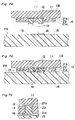
- Figs. 7A, 7B, and 7C the steps for mounting the electric circuit board CB obtained in a manner described above on a printed circuit board PB is described.
- the electric circuit board CB is placed over the printed circuit board PB such that conductor columns 13 are located over corresponding electrodes 16, as shown in Fig. 7A.
- the electric circuit board CB is pressed against the printed circuit board PB so that the surface of the substrate 15 is adhered tightly to adhesion layer 21a, as shown in Fig. 7B.
- the adhesion layers 21a and 21b, base layer 22 and conductor column 13 are deformed to contact with each other without any gap therebetween, as shown in Fig. 7C.
- the electric circuit board module CM is formed by a substrate 36, a plurality of electrodes 32, a plurality of conductor columns 33, and an adhesion layer 34 in a manner similar to that shown in Fig. 6.
- a first cover layer 34a is not removed from the adhesion layer 34.
- a protection layer 35 made of resinous material or paper, is additionally provided to cover the end surfaces of conductor columns 33.
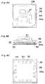
- the electric circuit board module CM further includes electric components 37 mounted thereon and electrically connected to the conductor columns 33 through the electrodes 32.
- the multilayer substrate ML includes a first dual-layer circuit substrate La.
- the first dual-layer circuit substrate has a construction very similar to that of the electric circuit board CB described with reference to Figs. 1A and 1B.
- a first substrate 41a, a first dual-layer electrode 42a, and a first adhesion layer 44a shown in Fig. 9A correspond to the substrate 11, electrode 12, conductor column 13, and adhesion layer 14 shown in Fig. 1A, respectively.
- the first substrate 41a is made of a resinous material, such as glass epoxy, and is provided with a plurality of first through holes 46a, each extending between the opposite surfaces thereof.
- Each of the first dual-layer electrodes 42a has electrode patterns on opposite surfaces of the first substrate 43a, and such electrode patterns are electrically connected by a ring shaped electrode segment extending along the first through hole 46a, as shown.
- the multilayer substrate ML further includes a second dual-layer circuit substrate Lb and a third dual-layer circuit substrate 41c.
- the second dual-layer circuit substrate Lb has a second substrate 41b with a plurality of second through holes 46b, a plurality of second dual-layer electrode 42b, and a second adhesion layer 44b and has a construction similar to that of the first dual-layer circuit substrate La, as shown in Fig. 9A.
- the third dual-layer circuit substrate Lc has a third substrate 41c with a plurality of third through holes 46c and a plurality of third dual-layer electrodes 42c.
- the third dual-layer circuit substrate Lc has a construction similar to the first dual-layer circuit substrate 41a, but the conductor columns 43a and adhesion layer 44a are removed therefrom.
- Three dual-layer circuit substrates La, Lb, and Lc are pressed against each other, and are held together by the first and second adhesion layers 44a and 44b, to produce the multilayer substrate ML, as shown in Fig. 9A.
- the first, second, and third dual-layer electrodes 42a, 42b, and 42c are electrically connected via inner conductor columns 43a and 43b.
- electrode E1 and E2 are connected through column C1
- electrodes E2 and E3 are connected through column C2.
Landscapes
- Engineering & Computer Science (AREA)
- Manufacturing & Machinery (AREA)
- Microelectronics & Electronic Packaging (AREA)
- Combinations Of Printed Boards (AREA)
- Electric Connection Of Electric Components To Printed Circuits (AREA)
- Production Of Multi-Layered Print Wiring Board (AREA)
- Structures For Mounting Electric Components On Printed Circuit Boards (AREA)
Applications Claiming Priority (2)
| Application Number | Priority Date | Filing Date | Title |
|---|---|---|---|
| JP225930/91 | 1991-09-05 | ||
| JP3225930A JPH0567869A (ja) | 1991-09-05 | 1991-09-05 | 電装部品接合方法並びにモジユール及び多層基板 |
Publications (2)
| Publication Number | Publication Date |
|---|---|
| EP0530840A1 true EP0530840A1 (de) | 1993-03-10 |
| EP0530840B1 EP0530840B1 (de) | 1996-01-10 |
Family
ID=16837124
Family Applications (1)
| Application Number | Title | Priority Date | Filing Date |
|---|---|---|---|
| EP92115238A Expired - Lifetime EP0530840B1 (de) | 1991-09-05 | 1992-09-05 | Elektrische Leiterplattenbaugruppe und Herstellungsverfahren für eine elektrische Leiterplattenbaugruppe |
Country Status (5)
| Country | Link |
|---|---|
| US (1) | US5406459A (de) |
| EP (1) | EP0530840B1 (de) |
| JP (1) | JPH0567869A (de) |
| KR (1) | KR0142178B1 (de) |
| DE (1) | DE69207520T2 (de) |
Cited By (15)
| Publication number | Priority date | Publication date | Assignee | Title |
|---|---|---|---|---|
| EP0645951A1 (de) * | 1993-09-22 | 1995-03-29 | Matsushita Electric Industrial Co., Ltd. | Leiterplatte und Verfahren zu ihrer Herstellung |
| EP0645950A1 (de) * | 1993-09-21 | 1995-03-29 | Matsushita Electric Industrial Co., Ltd. | Verbindungsteil eines Schaltungssubstrats und Verfahren zur Herstellung mehrschichtiger Schaltungssubstrate unter Verwendung dieses Teils |
| WO1998004107A1 (en) * | 1996-07-23 | 1998-01-29 | Minnesota Mining And Manufacturing Company | Z-axis interconnect method and circuit |
| FR2766615A1 (fr) * | 1997-03-27 | 1999-01-29 | Nec Corp | Assemblage de circuit electronique et son procede de fabrication |
| WO1999009795A1 (en) * | 1997-08-13 | 1999-02-25 | Fry's Metals, Inc. | Process for the formation of composite films |
| WO2000032021A1 (en) * | 1998-11-19 | 2000-06-02 | Alliedsignal Inc. | Printed circuit assembly having locally enhanced wiring density |
| WO2001063989A1 (en) * | 2000-02-22 | 2001-08-30 | Honeywell International Inc. | Bond ply structure and associated process for interconnection of circuit layer pairs with conductive inks |
| US6510059B2 (en) | 1999-12-17 | 2003-01-21 | Matsushita Electric Industrial Co., Ltd. | Conductive resin, electronic module using conductive resin, and method of manufacturing electronic module |
| WO2003017367A1 (en) * | 2001-08-17 | 2003-02-27 | Virtual Integration, Inc. | Microelectronic packages including thin film decal and dielectric adhesive layer having conductive vias therein, and methods of fabricating the same |
| EP1213952A3 (de) * | 2000-12-05 | 2004-06-30 | Matsushita Electric Industrial Co., Ltd. | Schaltungssubstrat und Verfahren zu dessen Herstellung |
| EP1220589A3 (de) * | 2000-12-26 | 2004-07-21 | Denso Corporation | Gedruckte Leiterplatte und Verfahren zur Herstellung einer gedruckten Leiterplatte |
| EP1482547A3 (de) * | 2003-05-27 | 2009-08-19 | Xerox Corporation | Abstandshalter/Maske für eine elektische Verbindung |
| CN101483970B (zh) * | 2008-01-10 | 2010-12-08 | 欣兴电子股份有限公司 | 线路板 |
| WO2013128197A1 (en) * | 2012-03-02 | 2013-09-06 | Novalia Ltd | Circuit board assembly |
| WO2016037738A1 (de) * | 2014-09-08 | 2016-03-17 | Robert Bosch Gmbh | Verfahren zum herstellen eines elektronikmoduls insbesondere für ein kfz- getriebesteuergerät |
Families Citing this family (19)
| Publication number | Priority date | Publication date | Assignee | Title |
|---|---|---|---|---|
| US5612512A (en) * | 1992-11-11 | 1997-03-18 | Murata Manufacturing Co., Ltd. | High frequency electronic component having base substrate formed of bismaleimide-triazine resin and resistant film formed on base substrate |
| US5479694A (en) | 1993-04-13 | 1996-01-02 | Micron Technology, Inc. | Method for mounting integrated circuits onto printed circuit boards and testing |
| US5548091A (en) * | 1993-10-26 | 1996-08-20 | Tessera, Inc. | Semiconductor chip connection components with adhesives and methods for bonding to the chip |
| JPH08167630A (ja) * | 1994-12-15 | 1996-06-25 | Hitachi Ltd | チップ接続構造 |
| JP2833521B2 (ja) * | 1995-05-18 | 1998-12-09 | 日本電気株式会社 | 配線基板 |
| US6551845B1 (en) * | 1996-01-02 | 2003-04-22 | Micron Technology, Inc. | Method of temporarily securing a die to a burn-in carrier |
| US6460245B1 (en) | 1996-03-07 | 2002-10-08 | Tessera, Inc. | Method of fabricating semiconductor chip assemblies |
| US5936847A (en) * | 1996-05-02 | 1999-08-10 | Hei, Inc. | Low profile electronic circuit modules |
| US6163957A (en) * | 1998-11-13 | 2000-12-26 | Fujitsu Limited | Multilayer laminated substrates with high density interconnects and methods of making the same |
| RU2134498C1 (ru) * | 1998-12-08 | 1999-08-10 | Таран Александр Иванович | Контактный узел |
| US6326555B1 (en) | 1999-02-26 | 2001-12-04 | Fujitsu Limited | Method and structure of z-connected laminated substrate for high density electronic packaging |
| US6271107B1 (en) | 1999-03-31 | 2001-08-07 | Fujitsu Limited | Semiconductor with polymeric layer |
| JP4479083B2 (ja) * | 2000-10-03 | 2010-06-09 | パナソニック株式会社 | 誘電体フィルタ及び端子 |
| TW530377B (en) * | 2002-05-28 | 2003-05-01 | Via Tech Inc | Structure of laminated substrate with high integration and method of production thereof |
| WO2010146524A1 (en) * | 2009-06-19 | 2010-12-23 | Koninklijke Philips Electronics N.V. | Conformable electronic devices and methods for their manufacture |
| JP5426310B2 (ja) * | 2009-10-09 | 2014-02-26 | 藤倉化成株式会社 | 電子部品の実装方法および実装体 |
| KR20120110193A (ko) * | 2011-03-29 | 2012-10-10 | 삼성전자주식회사 | 불순물 도핑 방법 및 이를 이용한 씨모스 이미지 센서의 제조 방법 |
| WO2015052780A1 (ja) * | 2013-10-08 | 2015-04-16 | リンテック株式会社 | 電子部品実装体の製造方法 |
| US10820416B2 (en) * | 2015-11-27 | 2020-10-27 | Sony Corporation | Substrate apparatus and method of manufacturing the same |
Citations (3)
| Publication number | Priority date | Publication date | Assignee | Title |
|---|---|---|---|---|
| DE3439047A1 (de) * | 1984-10-25 | 1986-04-30 | Wilde Membran Impuls Technik GmbH, 5828 Ennepetal | Verfahren zur bestueckung einer schaltungsanordnung mit elektronischen bauteilen |
| US4928387A (en) * | 1989-09-07 | 1990-05-29 | Rockwell International Corp. | Temporary soldering aid for manufacture of printed wiring assemblies |
| DE9105035U1 (de) * | 1991-04-24 | 1992-06-17 | Siemens AG, 8000 München | Mehrlagen-Leiterplatte |
Family Cites Families (7)
| Publication number | Priority date | Publication date | Assignee | Title |
|---|---|---|---|---|
| US3795047A (en) * | 1972-06-15 | 1974-03-05 | Ibm | Electrical interconnect structuring for laminate assemblies and fabricating methods therefor |
| FR2505094A1 (fr) * | 1981-04-29 | 1982-11-05 | Trt Telecom Radio Electr | Procede de realisation des circuits hyperfrequences |
| JPS61229389A (ja) * | 1985-04-03 | 1986-10-13 | イビデン株式会社 | セラミツク配線板およびその製造方法 |
| US4803450A (en) * | 1987-12-14 | 1989-02-07 | General Electric Company | Multilayer circuit board fabricated from silicon |
| JPH02198198A (ja) * | 1989-01-27 | 1990-08-06 | Cmk Corp | 電磁波シールド層を備えるプリント配線板 |
| DE9015206U1 (de) * | 1990-11-05 | 1991-01-17 | Isabellenhütte Heusler GmbH KG, 6340 Dillenburg | Widerstandsanordnung in SMD-Bauweise |
| JP2562661Y2 (ja) * | 1992-10-13 | 1998-02-16 | 株式会社村田製作所 | 圧電素子の実装構造 |
-
1991
- 1991-09-05 JP JP3225930A patent/JPH0567869A/ja active Pending
-
1992
- 1992-09-02 US US07/939,000 patent/US5406459A/en not_active Expired - Lifetime
- 1992-09-05 DE DE69207520T patent/DE69207520T2/de not_active Expired - Fee Related
- 1992-09-05 KR KR1019920016171A patent/KR0142178B1/ko not_active Expired - Fee Related
- 1992-09-05 EP EP92115238A patent/EP0530840B1/de not_active Expired - Lifetime
Patent Citations (3)
| Publication number | Priority date | Publication date | Assignee | Title |
|---|---|---|---|---|
| DE3439047A1 (de) * | 1984-10-25 | 1986-04-30 | Wilde Membran Impuls Technik GmbH, 5828 Ennepetal | Verfahren zur bestueckung einer schaltungsanordnung mit elektronischen bauteilen |
| US4928387A (en) * | 1989-09-07 | 1990-05-29 | Rockwell International Corp. | Temporary soldering aid for manufacture of printed wiring assemblies |
| DE9105035U1 (de) * | 1991-04-24 | 1992-06-17 | Siemens AG, 8000 München | Mehrlagen-Leiterplatte |
Cited By (23)
| Publication number | Priority date | Publication date | Assignee | Title |
|---|---|---|---|---|
| EP0645950A1 (de) * | 1993-09-21 | 1995-03-29 | Matsushita Electric Industrial Co., Ltd. | Verbindungsteil eines Schaltungssubstrats und Verfahren zur Herstellung mehrschichtiger Schaltungssubstrate unter Verwendung dieses Teils |
| US6108903A (en) * | 1993-09-21 | 2000-08-29 | Matsushita Electric Industrial Co., Ltd. | Connecting member of a circuit substrate and method of manufacturing multilayer circuit substrates by using the same |
| US5972482A (en) * | 1993-09-22 | 1999-10-26 | Matsushita Electric Industrial Co., Ltd. | Printed circuit board and method of manufacturing the same |
| US6211487B1 (en) | 1993-09-22 | 2001-04-03 | Matsushita Electric Industrial Co., Ltd. | Printed circuit board and method of manufacturing the same |
| EP0645951A1 (de) * | 1993-09-22 | 1995-03-29 | Matsushita Electric Industrial Co., Ltd. | Leiterplatte und Verfahren zu ihrer Herstellung |
| US6326694B1 (en) | 1993-09-22 | 2001-12-04 | Matsushita Electric Industrial Co., Ltd. | Printed circuit board |
| WO1998004107A1 (en) * | 1996-07-23 | 1998-01-29 | Minnesota Mining And Manufacturing Company | Z-axis interconnect method and circuit |
| US5873161A (en) * | 1996-07-23 | 1999-02-23 | Minnesota Mining And Manufacturing Company | Method of making a Z axis interconnect circuit |
| FR2766615A1 (fr) * | 1997-03-27 | 1999-01-29 | Nec Corp | Assemblage de circuit electronique et son procede de fabrication |
| WO1999009795A1 (en) * | 1997-08-13 | 1999-02-25 | Fry's Metals, Inc. | Process for the formation of composite films |
| WO2000032021A1 (en) * | 1998-11-19 | 2000-06-02 | Alliedsignal Inc. | Printed circuit assembly having locally enhanced wiring density |
| US6510059B2 (en) | 1999-12-17 | 2003-01-21 | Matsushita Electric Industrial Co., Ltd. | Conductive resin, electronic module using conductive resin, and method of manufacturing electronic module |
| WO2001063989A1 (en) * | 2000-02-22 | 2001-08-30 | Honeywell International Inc. | Bond ply structure and associated process for interconnection of circuit layer pairs with conductive inks |
| US6576839B1 (en) | 2000-02-22 | 2003-06-10 | Honeywell International Inc. | Bond-ply structure for interconnection of circuit layer pairs with conductive inks |
| EP1213952A3 (de) * | 2000-12-05 | 2004-06-30 | Matsushita Electric Industrial Co., Ltd. | Schaltungssubstrat und Verfahren zu dessen Herstellung |
| US6930395B2 (en) | 2000-12-05 | 2005-08-16 | Matsushita Electric Industrial Co., Ltd. | Circuit substrate having improved connection reliability and a method for manufacturing the same |
| EP1220589A3 (de) * | 2000-12-26 | 2004-07-21 | Denso Corporation | Gedruckte Leiterplatte und Verfahren zur Herstellung einer gedruckten Leiterplatte |
| US7188412B2 (en) | 2000-12-26 | 2007-03-13 | Denso Corporation | Method for manufacturing printed wiring board |
| WO2003017367A1 (en) * | 2001-08-17 | 2003-02-27 | Virtual Integration, Inc. | Microelectronic packages including thin film decal and dielectric adhesive layer having conductive vias therein, and methods of fabricating the same |
| EP1482547A3 (de) * | 2003-05-27 | 2009-08-19 | Xerox Corporation | Abstandshalter/Maske für eine elektische Verbindung |
| CN101483970B (zh) * | 2008-01-10 | 2010-12-08 | 欣兴电子股份有限公司 | 线路板 |
| WO2013128197A1 (en) * | 2012-03-02 | 2013-09-06 | Novalia Ltd | Circuit board assembly |
| WO2016037738A1 (de) * | 2014-09-08 | 2016-03-17 | Robert Bosch Gmbh | Verfahren zum herstellen eines elektronikmoduls insbesondere für ein kfz- getriebesteuergerät |
Also Published As
| Publication number | Publication date |
|---|---|
| KR0142178B1 (ko) | 1998-07-15 |
| US5406459A (en) | 1995-04-11 |
| DE69207520D1 (de) | 1996-02-22 |
| EP0530840B1 (de) | 1996-01-10 |
| DE69207520T2 (de) | 1996-08-29 |
| JPH0567869A (ja) | 1993-03-19 |
Similar Documents
| Publication | Publication Date | Title |
|---|---|---|
| EP0530840B1 (de) | Elektrische Leiterplattenbaugruppe und Herstellungsverfahren für eine elektrische Leiterplattenbaugruppe | |
| US6147311A (en) | Multi layer circuit board using anisotropic electroconductive adhesive layer and method for producing same | |
| US6977441B2 (en) | Interconnect substrate and method of manufacture thereof, electronic component and method of manufacturing thereof, circuit board and electronic instrument | |
| US7376318B2 (en) | Circuit board and its manufacturing method | |
| US6169253B1 (en) | Solder resist window configurations for solder paste overprinting | |
| EP0653789A2 (de) | Elektronische Gehäusungsstruktur und ihre Herstellung | |
| US5172852A (en) | Soldering method | |
| US6243946B1 (en) | Method of forming an interlayer connection structure | |
| KR20010092350A (ko) | 전자 회로 장치 | |
| KR100556240B1 (ko) | 반도체 장치 제조방법 | |
| JPH0823160A (ja) | プリント配線板と電子部品の接続方法 | |
| JP3472299B2 (ja) | 多層回路ユニットの製造方法及びその構成要素 | |
| KR20020077916A (ko) | 회로 기판 모듈의 제조 방법 | |
| JPH0563112B2 (de) | ||
| JPH07201634A (ja) | セラミックチップ部品 | |
| JP3560996B2 (ja) | 実装用配線板およびこれを用いた実装方法 | |
| US4734672A (en) | Variable resistor circuit module and method of manufacture | |
| JPS62296495A (ja) | 部品を制御回路上の表面のはんだパツドに取付ける方法 | |
| JPH03129745A (ja) | 半導体装置の実装方法 | |
| JPS6255717B2 (de) | ||
| JPH0734511B2 (ja) | 多層基板の電子部品実装構造及びその実装方法 | |
| KR100275440B1 (ko) | 전도성 필림을 이용한 회로기판의 실장 방법 및 지그 | |
| JP2980402B2 (ja) | 回路部品搭載用中間基板の製造法 | |
| JPH0458189B2 (de) | ||
| JP2001345592A (ja) | 電子部品及びその製造方法 |
Legal Events
| Date | Code | Title | Description |
|---|---|---|---|
| PUAI | Public reference made under article 153(3) epc to a published international application that has entered the european phase |
Free format text: ORIGINAL CODE: 0009012 |
|
| 17P | Request for examination filed |
Effective date: 19920905 |
|
| AK | Designated contracting states |
Kind code of ref document: A1 Designated state(s): DE FR GB |
|
| 17Q | First examination report despatched |
Effective date: 19940714 |
|
| GRAA | (expected) grant |
Free format text: ORIGINAL CODE: 0009210 |
|
| AK | Designated contracting states |
Kind code of ref document: B1 Designated state(s): DE FR GB |
|
| REF | Corresponds to: |
Ref document number: 69207520 Country of ref document: DE Date of ref document: 19960222 |
|
| ET | Fr: translation filed | ||
| PLBE | No opposition filed within time limit |
Free format text: ORIGINAL CODE: 0009261 |
|
| 26N | No opposition filed | ||
| REG | Reference to a national code |
Ref country code: GB Ref legal event code: IF02 |
|
| PGFP | Annual fee paid to national office [announced via postgrant information from national office to epo] |
Ref country code: GB Payment date: 20060830 Year of fee payment: 15 |
|
| PGFP | Annual fee paid to national office [announced via postgrant information from national office to epo] |
Ref country code: DE Payment date: 20060831 Year of fee payment: 15 |
|
| PGFP | Annual fee paid to national office [announced via postgrant information from national office to epo] |
Ref country code: FR Payment date: 20060908 Year of fee payment: 15 |
|
| GBPC | Gb: european patent ceased through non-payment of renewal fee |
Effective date: 20070905 |
|
| PG25 | Lapsed in a contracting state [announced via postgrant information from national office to epo] |
Ref country code: DE Free format text: LAPSE BECAUSE OF NON-PAYMENT OF DUE FEES Effective date: 20080401 |
|
| REG | Reference to a national code |
Ref country code: FR Ref legal event code: ST Effective date: 20080531 |
|
| PG25 | Lapsed in a contracting state [announced via postgrant information from national office to epo] |
Ref country code: FR Free format text: LAPSE BECAUSE OF NON-PAYMENT OF DUE FEES Effective date: 20071001 |
|
| PG25 | Lapsed in a contracting state [announced via postgrant information from national office to epo] |
Ref country code: GB Free format text: LAPSE BECAUSE OF NON-PAYMENT OF DUE FEES Effective date: 20070905 |