EP0532211A1 - Röntgenlithographische Maske und Verwendung zur Herstellung einer Halbleitervorrichtung - Google Patents
Röntgenlithographische Maske und Verwendung zur Herstellung einer Halbleitervorrichtung Download PDFInfo
- Publication number
- EP0532211A1 EP0532211A1 EP92307864A EP92307864A EP0532211A1 EP 0532211 A1 EP0532211 A1 EP 0532211A1 EP 92307864 A EP92307864 A EP 92307864A EP 92307864 A EP92307864 A EP 92307864A EP 0532211 A1 EP0532211 A1 EP 0532211A1
- Authority
- EP
- European Patent Office
- Prior art keywords
- mask
- substrate
- ray mask
- ray
- wafer
- Prior art date
- Legal status (The legal status is an assumption and is not a legal conclusion. Google has not performed a legal analysis and makes no representation as to the accuracy of the status listed.)
- Granted
Links
Images



Classifications
-
- G—PHYSICS
- G03—PHOTOGRAPHY; CINEMATOGRAPHY; ANALOGOUS TECHNIQUES USING WAVES OTHER THAN OPTICAL WAVES; ELECTROGRAPHY; HOLOGRAPHY
- G03F—PHOTOMECHANICAL PRODUCTION OF TEXTURED OR PATTERNED SURFACES, e.g. FOR PRINTING, FOR PROCESSING OF SEMICONDUCTOR DEVICES; MATERIALS THEREFOR; ORIGINALS THEREFOR; APPARATUS SPECIALLY ADAPTED THEREFOR
- G03F1/00—Originals for photomechanical production of textured or patterned surfaces, e.g., masks, photo-masks, reticles; Mask blanks or pellicles therefor; Containers specially adapted therefor; Preparation thereof
- G03F1/22—Masks or mask blanks for imaging by radiation of 100nm or shorter wavelength, e.g. X-ray masks, extreme ultraviolet [EUV] masks; Preparation thereof
-
- G—PHYSICS
- G03—PHOTOGRAPHY; CINEMATOGRAPHY; ANALOGOUS TECHNIQUES USING WAVES OTHER THAN OPTICAL WAVES; ELECTROGRAPHY; HOLOGRAPHY
- G03F—PHOTOMECHANICAL PRODUCTION OF TEXTURED OR PATTERNED SURFACES, e.g. FOR PRINTING, FOR PROCESSING OF SEMICONDUCTOR DEVICES; MATERIALS THEREFOR; ORIGINALS THEREFOR; APPARATUS SPECIALLY ADAPTED THEREFOR
- G03F7/00—Photomechanical, e.g. photolithographic, production of textured or patterned surfaces, e.g. printing surfaces; Materials therefor, e.g. comprising photoresists; Apparatus specially adapted therefor
- G03F7/70—Microphotolithographic exposure; Apparatus therefor
- G03F7/70691—Handling of masks or workpieces
- G03F7/707—Chucks, e.g. chucking or un-chucking operations or structural details
-
- G—PHYSICS
- G03—PHOTOGRAPHY; CINEMATOGRAPHY; ANALOGOUS TECHNIQUES USING WAVES OTHER THAN OPTICAL WAVES; ELECTROGRAPHY; HOLOGRAPHY
- G03F—PHOTOMECHANICAL PRODUCTION OF TEXTURED OR PATTERNED SURFACES, e.g. FOR PRINTING, FOR PROCESSING OF SEMICONDUCTOR DEVICES; MATERIALS THEREFOR; ORIGINALS THEREFOR; APPARATUS SPECIALLY ADAPTED THEREFOR
- G03F7/00—Photomechanical, e.g. photolithographic, production of textured or patterned surfaces, e.g. printing surfaces; Materials therefor, e.g. comprising photoresists; Apparatus specially adapted therefor
- G03F7/70—Microphotolithographic exposure; Apparatus therefor
- G03F7/708—Construction of apparatus, e.g. environment aspects, hygiene aspects or materials
- G03F7/70858—Environment aspects, e.g. pressure of beam-path gas, temperature
- G03F7/70866—Environment aspects, e.g. pressure of beam-path gas, temperature of mask or workpiece
Definitions
- the present invention relates to an X-ray mask used in a semiconductor exposure device using an X-ray source, a method of manufacturing the X-ray mask and a semiconductor device manufacturing method using the X-ray mask.
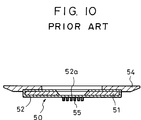
- an X-ray mask substrate 50 is joined to a mask frame 54.
- the X-ray mask substrate is produced by depositing an inorganic film 52 of SiN or the like on the surface of a silicon substrate 51, removing a portion corresponding to a permeable film portion 52a by dry etching, and removing a portion of the silicon substrate 51 which corresponds to the permeable film portion 52a by wet etching.
- a pattern 55 made of an X-ray absorber such as Ta, Au or the like is provided on the permeable film portion 52a in correspondence with a predetermined shape to be transferred to a wafer (not shown).
- the surface of the X-mask in which the pattern is formed is opposed to a wafer at a distance of about 30 ⁇ m.
- a portion of the wafer is exposed to light.
- the distance between the X-ray mask and the wafer is increased to about 200 ⁇ m, and the X-ray mask is then moved to a position corresponding to the other portion.
- the distance between the X-ray mask and the wafer is then returned to about 30 ⁇ m, and the other portion is exposed.
- the step-and-repeat operation is successively repeated to expose the wafer.
- the present invention has been achieved for solving the above problems. It is a first object of the present invention to provide an X-ray mask and a method of producing the X-ray mask which permits an increase in the speed of movement thereof without breaking or damaging a permeable film portion and which increases the productivity of the exposure process.
- the X-ray mask of this embodiment comprises a disk-like mask frame 4 having an opening concentrically formed at the center thereof, and an X-ray mask substrate 8 joined to the surface of the mask frame 4 and having a diameter greater than the diameter of the opening of the mask frame 4.
- grooves 4a are radially formed at equal intervals in the plane of the mask frame 4 which is joined to the X-ray mask substrate 8, so that the grooves 4a connect the internal periphery of the mask frame 4 with the external periphery thereof and communicate with the through holes 3 below.
- the X-ray mask substrate 8 comprises a silicon substrate 1 having an inorganic film 2 of SiN or the like deposited on the surface thereof.
- the central portion of the silicon substrate 1 is rectangularly removed leaving the inorganic film 2 on the side opposite to the junction plane of the mask frame 4.
- a permeable film portion 2a (the shadowed portion shown in Fig. 1) comprising the inorganic film 2 on the side opposite to the junction plane is formed in the central portion of the silicon substrate 1.
- a pattern 5 (refer to Fig. 2(E)) made of an X-ray absorber such as Ta, Au or the like is provided on the permeable film portion 2a in correspondence with a predetermined shape to be transferred to a wafer.
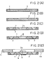
- the inorganic film 2 of SiN or the like is first deposited on the surface of the silicon substrate 1.
- a dry etching resist is then coated on the inorganic film 2, and portions of the resist which correspond to the permeable film portion 2a and the through holes 3 are removed by exposure to form a dry etching mask. As shown in Fig. 2(B), portions on the upper side of the inorganic film 2 which correspond to the permeable film portion 2a and the through holes 3 are removed by dry etching.
- portions of the silicon substrate 1 from which the inorganic film 2 is removed are removed by wet etching to form the permeable film portion 2a.
- the remaining portions of the inorganic film 2 which respectively correspond to the through holes 3 are removed to form the through holes 3.
- the X-ray mask substrate 8 is formed.
- the portions of the inorganic film 2 which are desired to be removed may be removed by wet etching or mechanical means using a cutter or the like.
- the pattern 5 made of an X-ray absorber such as Ta, Au or the like is then formed on the lower side of the inorganic film 2 shown in the drawing on the permeable film portion 2, and the through holes 3 are respectively aligned with the grooves 4a.
- the X-ray mask substrate 8 is joined to the mask frame 4 in parallel with each other by an adhesive.
- the X-ray mask 10 When exposure is performed using the X-ray mask of this embodiment, as shown in Fig. 3, the X-ray mask 10 vertically held by a mask chuck 6 is moved to the left of the drawing so as to be brought close to a wafer 7. At this time, the He gas present between the X-ray mask 10 and the wafer 7 passes through the through holes 3 and the grooves 4a and flows to the side of the X-ray mask 10 and to the mask chuck 6. Thus the pressure of the He gas present between the X-ray mask and the wafer 7 is not increased, and if the X-ray mask 10 is rapidly brought close to the wafer 7, there is no danger of breaking the permeable film portion 2a serving as a permeable support film.
- the number of through holes or grooves is not limited to 4, and can be changed according to demand.
- the grooves 4a need not be provided, and through holes may be formed in the mask frame 4 in place of the grooves 4a.
- shielding is provided to prevent X-rays from leaking from the through holes.
- the X-ray mask of this embodiment comprises a disk-like mask frame 14 having an opening concentrically formed in the central portion thereof, and a square plate X-ray mask substrate 18 joined to the surface of the mask frame 14.
- the X-ray mask substrate 18 comprises a silicon substrate 11 having an inorganic film 12 formed on the surface thereof.
- the X-ray mask substrate 18 also has a permeable film portion 12a (the shadowed portion shown in the drawing) formed in the central portion thereof.
- the length of the diagonal of the X-ray mask substrate 18 is greater than the diameter of the opening of the mask frame 14, and the length of one side of the X-ray mask substrate 18 is smaller than the diameter of the opening of the mask frame 14. In the state where the X-ray mask 18 is joined to the mask frame 14, the opening of the mask frame 14 is thus not closed by the X-ray mask substrate 18, thereby forming gaps 13 serving as gas passages between the opening and the X-ray mask 18.
- the permeable film portion 12a may be configured in the same way as that in the first embodiment, it is not described below.
- the inorganic film 12 of SiN or the like is deposited on the surface of the silicon substrate 11.
- a dry etching resist is then coated on the inorganic film 12, and portions of the resist corresponding to the permeable film portion and the circumference thereof are removed by exposure to form a dry etching mask. As shown in Fig. 5(B), portions of the inorganic film 12 on the upper side thereof, which correspond to the permeable film portion and the circumference thereof, are removed by dry etching.
- portions of the silicon substrate 11 from which the inorganic film 12 is removed are removed by wet etching to form the permeable film portion 12a.
- the portions of the inorganic film 12 which remain in the circumference are removed to form the X-ray mask substrate 11.
- a portion of the inorganic film 12 which is desired to be removed may be removed by wet etching or mechanical means using a cutter or the like.
- a pattern 15 made of an X-ray absorber such as Ta, Au or the like is formed on the lower side of the inorganic film 12 on the permeable film portion 12a shown in the drawing, and the X-ray mask substrate 11 is joined to the mask frame 14 in parallel with each other by an adhesive.
- the He gas present between the X-ray mask 20 and the wafer 17 passes through each of the gaps 13 and flows to the mask chuck 16, as shown by arrows in the drawing.
- the pressure of the He gas present between the X-ray mask 20 and the wafer 17 is not increased, and there is no danger of breaking the permeable film portion 12a serving as a permeable support film even if the X-ray mask 20 is rapidly brought close to the wafer 17.
- the X-ray mask substrate 18 has a necessary minimum configuration including the permeable film portion 12a, it is possible to decrease the weight of the X-ray mask 20 and decrease the load on a mask conveyance system comprising a mask hand or the like in an exposure device.
- the mask conveyance system can be consequently decreased in size and weight.
- the flatness of the plane of the X-ray mask 20 which faces the wafer 17 can be improved.
- the X-ray mask substrate 18 and the opening of the mask frame 14 have a rectangular shape and a circular shape, respectively, both shapes may be interchanged. Any desired shape can be selected unless the opening is closed by the X-ray mask substrate 18 when the X-ray mask substrate 18 is joined to the mask frame 14.
- the X-ray mask substrate has gas passages provided in the perimeter of the permeable film portion so as to connect the one side of the substrate with the other side thereof. This causes the gas present between the X-ray mask and the wafer to pass through the gas passages and flow to the other side of the X-ray mask substrate when the X-ray mask is moved toward the wafer during exposure, without increasing the pressure between the X-ray mask and the wafer. Since there is thus no danger of breaking the permeable film portion, it is possible to increase the speed of movement of the X-ray mask and improve the productivity of the exposure device. This is significantly effective for step-and-repeat type exposure. In addition, since the weight of the X-ray mask is decreased by providing the gas passages in the X-ray mask substrate, the mask conveyance system of the exposure device can be decreased in size and weight.
- the grooves are radially formed in the surface of the mask frame which is joined to the X-ray mask substrate so as to communicate with the gas passages so that when the X-ray mask is moved toward the wafer, the gas present between the X-ray mask and the wafer can be effectively made to escape from the spaces between the X-ray mask and the wafer.
- the gas present between the X-ray mask and the wafer passes through the gaps and flows to the other side of the X-ray mask substrate, without increasing the pressure between the X-ray mask and the wafer. Since there is thus no danger of breaking the permeable film portion, it is possible to increase the speed of movement of the X-ray mask and improve the productivity of the exposure device. Since the X-ray mask substrate has a necessary minimum structure outside of the circumference of the permeable film portion, the X-ray mask substrate can be decreased in weight, and the mask conveyance system of the exposure device can be decreased in size and weight. The smallness of the area of the surface of the X-ray mask substrate which faces the wafer during exposure permits improvement in the flatness of the surface.
- the gas passages are formed by removing the inorganic film remaining in the portions on the other side of the silicon substrate, which correspond to the gas passages, in the same process as that for forming the permeable film portion.
- the gas passages can easily be formed by adding a simple step of removing the inorganic film in portions corresponding to the gas passages to a conventional method of manufacturing an X-ray mask substrate.
- FIG. 7 is a drawing showing the configuration of the X-ray exposure device of this embodiment.
- the sheet beam-like synchrotron radiation emitted from a radiation source 20 such as an SOR ring or the like is enlarged and reflected by a fixed convex mirror 22 in the direction (y direction) vertical to the radiation orbital plane so that the whole exposure region L o can be irradiated.
- X-rays are extracted from the synchrotron radiation 21 reflected and enlarged by the convex mirror 22, and exposure within the irradiation region is adjusted by a shutter 23 for controlling exposure.
- the X-rays passing through the shutter 23 are led to an X-ray mask 24 held by a mask chuck.
- the X-ray mask 24 has the same structure as that of the above-described embodiments.
- the circuit pattern formed on the X-ray permeable film portion of the X-ray mask 23 is projected on a silicon wafer 25 coated with a resist by step-and-repeat type exposure.
- the X-ray exposure device of this embodiment permits an increase in the speed of movement of the X-ray mask toward the wafer and thus has the effect of increasing the productivity. This effect is remarkable in step-and-repeat type exposure in which the operation of bringing the X-ray mask close to the wafer is repeated several times.
- Fig. 8 shows a manufacture flow for semiconductor devices (a semiconductor chip such as IC, LSI or the like, a liquid crystal panel, CCD or the like).
- Step 1 circuit design
- Step 2 mask manufacture
- Step 3 wafer manufacture
- Step 4 wafer process, which is called pre-process
- an actual circuit is formed on the wafer by lithography using the prepared mask and wafer.
- Step 5 assembly, called post-process
- the post-process comprising the assembly step (dicing, bonding), the packaging step (chip sealing) and the like.
- Step 6 tests of the semiconductor device formed in Step 5, such as the operation confirmation test, the durability test and the like, are carried out.
- the semiconductor devices completed through the above steps are shipped (Step 7).
- Fig. 9 shows the detailed flow of the above wafer process.
- Step 11 oxidation
- Step 12 CVD
- Step 13 electrode formation
- Step 14 ion implantation
- Step 15 resist process
- Step 16 exposure
- Step 18 etching
- Step 19 resist separation
Landscapes
- Physics & Mathematics (AREA)
- General Physics & Mathematics (AREA)
- Health & Medical Sciences (AREA)
- Life Sciences & Earth Sciences (AREA)
- Atmospheric Sciences (AREA)
- Toxicology (AREA)
- Engineering & Computer Science (AREA)
- Environmental & Geological Engineering (AREA)
- Epidemiology (AREA)
- Public Health (AREA)
- Preparing Plates And Mask In Photomechanical Process (AREA)
- Exposure And Positioning Against Photoresist Photosensitive Materials (AREA)
- Exposure Of Semiconductors, Excluding Electron Or Ion Beam Exposure (AREA)
Applications Claiming Priority (2)
| Application Number | Priority Date | Filing Date | Title |
|---|---|---|---|
| JP23032891A JPH0567561A (ja) | 1991-09-10 | 1991-09-10 | X線マスク基板とその製造方法およびx線マスク |
| JP230328/91 | 1991-09-10 |
Publications (2)
| Publication Number | Publication Date |
|---|---|
| EP0532211A1 true EP0532211A1 (de) | 1993-03-17 |
| EP0532211B1 EP0532211B1 (de) | 1997-12-29 |
Family
ID=16906116
Family Applications (1)
| Application Number | Title | Priority Date | Filing Date |
|---|---|---|---|
| EP92307864A Expired - Lifetime EP0532211B1 (de) | 1991-09-10 | 1992-08-28 | Röntgenlithographische Maske und Verwendung zur Herstellung einer Halbleitervorrichtung |
Country Status (6)
| Country | Link |
|---|---|
| US (1) | US5224139A (de) |
| EP (1) | EP0532211B1 (de) |
| JP (1) | JPH0567561A (de) |
| CA (1) | CA2077359C (de) |
| DE (1) | DE69223708T2 (de) |
| SG (1) | SG76477A1 (de) |
Families Citing this family (7)
| Publication number | Priority date | Publication date | Assignee | Title |
|---|---|---|---|---|
| ATE184711T1 (de) * | 1991-11-15 | 1999-10-15 | Canon Kk | Röntgenstrahlmaskenstruktur und - belichtungsverfahren sowie damit hergestelltes halbleiterbauelement und herstellungsverfahren für die röntgenstrahlmaskenstruktur |
| EP0677787B1 (de) * | 1994-03-15 | 1998-10-21 | Canon Kabushiki Kaisha | Maske und Maskenträger |
| US5509041A (en) * | 1994-06-30 | 1996-04-16 | Motorola, Inc. | X-ray lithography method for irradiating an object to form a pattern thereon |
| KR0170594B1 (ko) * | 1996-05-25 | 1999-03-20 | 양승택 | 마스크용 글래스 링 구조 |
| JP3332872B2 (ja) * | 1998-10-27 | 2002-10-07 | キヤノン株式会社 | 露光方法 |
| JP4735272B2 (ja) * | 2006-01-13 | 2011-07-27 | 日本精工株式会社 | 露光装置 |
| KR101041138B1 (ko) * | 2009-03-03 | 2011-06-13 | 삼성모바일디스플레이주식회사 | 증착용 마스크 |
Citations (3)
| Publication number | Priority date | Publication date | Assignee | Title |
|---|---|---|---|---|
| EP0278076A2 (de) * | 1987-02-06 | 1988-08-17 | Dr. Johannes Heidenhain GmbH | Bestrahlungsmaske zur lithographischen Erzeugung von Mustern |
| EP0385480A2 (de) * | 1989-03-02 | 1990-09-05 | Kabushiki Kaisha Toshiba | Aperturmusterdruckplatte für eine Schattenmaske und Herstellungsverfahren dafür |
| EP0452043A1 (de) * | 1990-04-09 | 1991-10-16 | Canon Kabushiki Kaisha | Röntgenstrahlen-Maskenstruktur |
Family Cites Families (1)
| Publication number | Priority date | Publication date | Assignee | Title |
|---|---|---|---|---|
| EP0244496B1 (de) * | 1986-05-06 | 1991-01-16 | Ibm Deutschland Gmbh | Maske für die Ionen-, Elektronen- oder Röntgenstrahllithographie und Verfahren zur ihrer Herstellung |
-
1991
- 1991-09-10 JP JP23032891A patent/JPH0567561A/ja active Pending
-
1992
- 1992-08-28 SG SG1996009021A patent/SG76477A1/en unknown
- 1992-08-28 US US07/936,510 patent/US5224139A/en not_active Expired - Fee Related
- 1992-08-28 DE DE69223708T patent/DE69223708T2/de not_active Expired - Fee Related
- 1992-08-28 EP EP92307864A patent/EP0532211B1/de not_active Expired - Lifetime
- 1992-09-02 CA CA002077359A patent/CA2077359C/en not_active Expired - Fee Related
Patent Citations (3)
| Publication number | Priority date | Publication date | Assignee | Title |
|---|---|---|---|---|
| EP0278076A2 (de) * | 1987-02-06 | 1988-08-17 | Dr. Johannes Heidenhain GmbH | Bestrahlungsmaske zur lithographischen Erzeugung von Mustern |
| EP0385480A2 (de) * | 1989-03-02 | 1990-09-05 | Kabushiki Kaisha Toshiba | Aperturmusterdruckplatte für eine Schattenmaske und Herstellungsverfahren dafür |
| EP0452043A1 (de) * | 1990-04-09 | 1991-10-16 | Canon Kabushiki Kaisha | Röntgenstrahlen-Maskenstruktur |
Non-Patent Citations (1)
| Title |
|---|
| PATENT ABSTRACTS OF JAPAN vol. 11, no. 173 (P-582)(2620) 4 June 1987 & JP-A-62 005 243 ( RICOH CO LTD ) 12 January 1987 * |
Also Published As
| Publication number | Publication date |
|---|---|
| DE69223708D1 (de) | 1998-02-05 |
| JPH0567561A (ja) | 1993-03-19 |
| US5224139A (en) | 1993-06-29 |
| DE69223708T2 (de) | 1998-04-23 |
| CA2077359C (en) | 1997-02-04 |
| EP0532211B1 (de) | 1997-12-29 |
| SG76477A1 (en) | 2000-11-21 |
| CA2077359A1 (en) | 1993-03-11 |
Similar Documents
| Publication | Publication Date | Title |
|---|---|---|
| US6097790A (en) | Pressure partition for X-ray exposure apparatus | |
| US6509247B2 (en) | Semiconductor device and alignment method | |
| US5485495A (en) | X-ray mask, and exposure apparatus and device production using the mask | |
| JP3244894B2 (ja) | マスク保持方法、マスク及びマスクチャック、ならびにこれを用いた露光装置とデバイス製造方法 | |
| US5224139A (en) | X-ray mask and semiconductor device manufacturing method using the same | |
| US4702592A (en) | Reticle assembly, system, and method for using the same | |
| US6069931A (en) | Mask structure and mask holding mechanism for exposure apparatus | |
| EP1431825A1 (de) | Lithographischer Apparat, Verfahren zur Herstellung einer Vorrichtung und Substrathalter | |
| JPH08330222A (ja) | X線露光用マスク及びそれを用いた半導体素子の製造方法 | |
| US4349621A (en) | Process for X-ray microlithography using thin film eutectic masks | |
| EP0677787B1 (de) | Maske und Maskenträger | |
| KR100412017B1 (ko) | 노광방법 및 이 방법용 x선마스크구조체 | |
| KR19990072348A (ko) | 개선된엑스-선마스크구조체 | |
| US5623529A (en) | SOR exposure system and mask manufactured thereby | |
| US6258492B1 (en) | X-ray mask structure and method of making the same | |
| JPH07167995A (ja) | 露光装置およびデバイス製造方法 | |
| US6645707B2 (en) | Device manufacturing method | |
| JP3278312B2 (ja) | マスク、マスク支持方法、マスク支持機構、並びにこれを用いた露光装置やデバイス製造方法 | |
| JPH06100825B2 (ja) | パタ−ン形成方法 | |
| JP3130419B2 (ja) | 位置決めステージ装置およびこれを用いた露光装置 | |
| JP3359330B2 (ja) | マスク保持方法とマスク、並びにこれを用いたデバイス製造方法 | |
| JPH10242032A (ja) | マスク保持装置、露光装置、デバイス製造方法、及びマスク構造体 | |
| EP1431831B1 (de) | Lithographischer Apparat, Verfahren zur Herstellung einer Vorrichtung und Substrathalter | |
| US6784974B1 (en) | Exposure method and exposure apparatus | |
| JPH1092736A (ja) | プロキシミティ露光装置 |
Legal Events
| Date | Code | Title | Description |
|---|---|---|---|
| PUAI | Public reference made under article 153(3) epc to a published international application that has entered the european phase |
Free format text: ORIGINAL CODE: 0009012 |
|
| AK | Designated contracting states |
Kind code of ref document: A1 Designated state(s): DE FR GB NL |
|
| 17P | Request for examination filed |
Effective date: 19930729 |
|
| 17Q | First examination report despatched |
Effective date: 19950818 |
|
| GRAG | Despatch of communication of intention to grant |
Free format text: ORIGINAL CODE: EPIDOS AGRA |
|
| GRAG | Despatch of communication of intention to grant |
Free format text: ORIGINAL CODE: EPIDOS AGRA |
|
| GRAH | Despatch of communication of intention to grant a patent |
Free format text: ORIGINAL CODE: EPIDOS IGRA |
|
| GRAH | Despatch of communication of intention to grant a patent |
Free format text: ORIGINAL CODE: EPIDOS IGRA |
|
| GRAA | (expected) grant |
Free format text: ORIGINAL CODE: 0009210 |
|
| AK | Designated contracting states |
Kind code of ref document: B1 Designated state(s): DE FR GB NL |
|
| REF | Corresponds to: |
Ref document number: 69223708 Country of ref document: DE Date of ref document: 19980205 |
|
| ET | Fr: translation filed | ||
| PLBE | No opposition filed within time limit |
Free format text: ORIGINAL CODE: 0009261 |
|
| STAA | Information on the status of an ep patent application or granted ep patent |
Free format text: STATUS: NO OPPOSITION FILED WITHIN TIME LIMIT |
|
| 26N | No opposition filed | ||
| REG | Reference to a national code |
Ref country code: GB Ref legal event code: IF02 |
|
| PGFP | Annual fee paid to national office [announced via postgrant information from national office to epo] |
Ref country code: DE Payment date: 20030828 Year of fee payment: 12 |
|
| PGFP | Annual fee paid to national office [announced via postgrant information from national office to epo] |
Ref country code: GB Payment date: 20040816 Year of fee payment: 13 |
|
| PGFP | Annual fee paid to national office [announced via postgrant information from national office to epo] |
Ref country code: FR Payment date: 20040827 Year of fee payment: 13 |
|
| PGFP | Annual fee paid to national office [announced via postgrant information from national office to epo] |
Ref country code: NL Payment date: 20040831 Year of fee payment: 13 |
|
| PG25 | Lapsed in a contracting state [announced via postgrant information from national office to epo] |
Ref country code: DE Free format text: LAPSE BECAUSE OF NON-PAYMENT OF DUE FEES Effective date: 20050301 |
|
| PG25 | Lapsed in a contracting state [announced via postgrant information from national office to epo] |
Ref country code: GB Free format text: LAPSE BECAUSE OF NON-PAYMENT OF DUE FEES Effective date: 20050828 |
|
| PG25 | Lapsed in a contracting state [announced via postgrant information from national office to epo] |
Ref country code: NL Free format text: LAPSE BECAUSE OF NON-PAYMENT OF DUE FEES Effective date: 20060301 |
|
| GBPC | Gb: european patent ceased through non-payment of renewal fee |
Effective date: 20050828 |
|
| PG25 | Lapsed in a contracting state [announced via postgrant information from national office to epo] |
Ref country code: FR Free format text: LAPSE BECAUSE OF NON-PAYMENT OF DUE FEES Effective date: 20060428 |
|
| NLV4 | Nl: lapsed or anulled due to non-payment of the annual fee |
Effective date: 20060301 |
|
| REG | Reference to a national code |
Ref country code: FR Ref legal event code: ST Effective date: 20060428 |