EP0452043A1 - Röntgenstrahlen-Maskenstruktur - Google Patents
Röntgenstrahlen-Maskenstruktur Download PDFInfo
- Publication number
- EP0452043A1 EP0452043A1 EP91302999A EP91302999A EP0452043A1 EP 0452043 A1 EP0452043 A1 EP 0452043A1 EP 91302999 A EP91302999 A EP 91302999A EP 91302999 A EP91302999 A EP 91302999A EP 0452043 A1 EP0452043 A1 EP 0452043A1
- Authority
- EP
- European Patent Office
- Prior art keywords
- supporting frame
- mask substrate
- mask
- adhesive agent
- mask structure
- Prior art date
- Legal status (The legal status is an assumption and is not a legal conclusion. Google has not performed a legal analysis and makes no representation as to the accuracy of the status listed.)
- Granted
Links
Images
Classifications
-
- G—PHYSICS
- G03—PHOTOGRAPHY; CINEMATOGRAPHY; ANALOGOUS TECHNIQUES USING WAVES OTHER THAN OPTICAL WAVES; ELECTROGRAPHY; HOLOGRAPHY
- G03F—PHOTOMECHANICAL PRODUCTION OF TEXTURED OR PATTERNED SURFACES, e.g. FOR PRINTING, FOR PROCESSING OF SEMICONDUCTOR DEVICES; MATERIALS THEREFOR; ORIGINALS THEREFOR; APPARATUS SPECIALLY ADAPTED THEREFOR
- G03F1/00—Originals for photomechanical production of textured or patterned surfaces, e.g., masks, photo-masks, reticles; Mask blanks or pellicles therefor; Containers specially adapted therefor; Preparation thereof
- G03F1/22—Masks or mask blanks for imaging by radiation of 100nm or shorter wavelength, e.g. X-ray masks, extreme ultraviolet [EUV] masks; Preparation thereof
-
- G—PHYSICS
- G03—PHOTOGRAPHY; CINEMATOGRAPHY; ANALOGOUS TECHNIQUES USING WAVES OTHER THAN OPTICAL WAVES; ELECTROGRAPHY; HOLOGRAPHY
- G03F—PHOTOMECHANICAL PRODUCTION OF TEXTURED OR PATTERNED SURFACES, e.g. FOR PRINTING, FOR PROCESSING OF SEMICONDUCTOR DEVICES; MATERIALS THEREFOR; ORIGINALS THEREFOR; APPARATUS SPECIALLY ADAPTED THEREFOR
- G03F7/00—Photomechanical, e.g. photolithographic, production of textured or patterned surfaces, e.g. printing surfaces; Materials therefor, e.g. comprising photoresists; Apparatus specially adapted therefor
- G03F7/70—Microphotolithographic exposure; Apparatus therefor
- G03F7/708—Construction of apparatus, e.g. environment aspects, hygiene aspects or materials
- G03F7/70858—Environment aspects, e.g. pressure of beam-path gas, temperature
- G03F7/70866—Environment aspects, e.g. pressure of beam-path gas, temperature of mask or workpiece
-
- Y—GENERAL TAGGING OF NEW TECHNOLOGICAL DEVELOPMENTS; GENERAL TAGGING OF CROSS-SECTIONAL TECHNOLOGIES SPANNING OVER SEVERAL SECTIONS OF THE IPC; TECHNICAL SUBJECTS COVERED BY FORMER USPC CROSS-REFERENCE ART COLLECTIONS [XRACs] AND DIGESTS
- Y10—TECHNICAL SUBJECTS COVERED BY FORMER USPC
- Y10T—TECHNICAL SUBJECTS COVERED BY FORMER US CLASSIFICATION
- Y10T428/00—Stock material or miscellaneous articles
- Y10T428/21—Circular sheet or circular blank
-
- Y—GENERAL TAGGING OF NEW TECHNOLOGICAL DEVELOPMENTS; GENERAL TAGGING OF CROSS-SECTIONAL TECHNOLOGIES SPANNING OVER SEVERAL SECTIONS OF THE IPC; TECHNICAL SUBJECTS COVERED BY FORMER USPC CROSS-REFERENCE ART COLLECTIONS [XRACs] AND DIGESTS
- Y10—TECHNICAL SUBJECTS COVERED BY FORMER USPC
- Y10T—TECHNICAL SUBJECTS COVERED BY FORMER US CLASSIFICATION
- Y10T428/00—Stock material or miscellaneous articles
- Y10T428/24—Structurally defined web or sheet [e.g., overall dimension, etc.]
- Y10T428/24479—Structurally defined web or sheet [e.g., overall dimension, etc.] including variation in thickness
- Y10T428/24612—Composite web or sheet
-
- Y—GENERAL TAGGING OF NEW TECHNOLOGICAL DEVELOPMENTS; GENERAL TAGGING OF CROSS-SECTIONAL TECHNOLOGIES SPANNING OVER SEVERAL SECTIONS OF THE IPC; TECHNICAL SUBJECTS COVERED BY FORMER USPC CROSS-REFERENCE ART COLLECTIONS [XRACs] AND DIGESTS
- Y10—TECHNICAL SUBJECTS COVERED BY FORMER USPC
- Y10T—TECHNICAL SUBJECTS COVERED BY FORMER US CLASSIFICATION
- Y10T428/00—Stock material or miscellaneous articles
- Y10T428/24—Structurally defined web or sheet [e.g., overall dimension, etc.]
- Y10T428/24802—Discontinuous or differential coating, impregnation or bond [e.g., artwork, printing, retouched photograph, etc.]
- Y10T428/24851—Intermediate layer is discontinuous or differential
Definitions
- This invention relates to an X-ray mask structure usable in an X-ray exposure apparatus for manufacture of semiconductor devices.
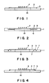
- Figure 1 shows an X-ray mask structure of known type.
- Denoted at 1 is a supporting frame
- denoted at 2 is a mask substrate
- denoted at 3 is an adhesive agent and denoted at 4 is a mask pattern.
- the mask substrate 2 is placed on the supporting frame 1, and the adhesive agent 3 is applied to the whole periphery of the mask substrate, whereby it is held fixed.
- the supporting frame 1 has a ring-like shape having an opening 15 formed at its center.
- the mask pattern 4 is formed of an X-ray absorptive material such as Au, for example, and it is formed on a thin film of a few micron thickness, made of an inorganic material such as SiN or SiC, for example.
- the mask substrate is formed of an inorganic material such as SiN or SiC, for example.
- the thin film can be formed by back-etching the mask substrate.
- the supporting frame 1 is provided by a Ti plate of a thickness of about 0.5 - 3 mm.
- Figure 2 shows another X-ray mask structure of known type.
- a recess 5 is formed in a supporting frame 1 and, in this recess 5, a mask substrate 2 is held fixed by using an adhesive agent layer 6.
- an X-ray mask having a mask pattern formed thereon includes an X-ray mask substrate on which the mask pattern is formed and a supporting frame for carrying and supporting the mask substrate, wherein the mask substrate is fixed to the supporting frame by means of an adhesive agent and wherein at least one of the mask substrate and the supporting frame is formed with a groove effective to release a stress in the mask structure.
- Figure 1 is a sectional view of an X-ray mask structure of known type.
- Figure 2 is a sectional view of another X-ray mask structure of known type.
- Figure 3 is a sectional view of an X-ray mask structure according to a first embodiment of the present invention.
- Figure 4 is a sectional view of an X-ray mask structure according to a second embodiment of the present invention.
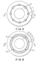
- Figure 5 is a top plan view of a supporting frame of the Figure 3 embodiment.
- Figure 6 is a top plan view of a supporting frame, in a modified form of the Figure 3 embodiment.
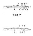
- Figure 7 is a sectional view of an X-ray mask structure according to a third embodiment of the present invention.
- Figure 8 is a sectional view of an X-ray mask structure according to a fourth embodiment of the present invention.
- Figure 1 shows a first embodiment of the present invention. Like numerals as those of Figure 1 are assigned to similar or corresponding elements, and explanation therefor is omitted here.
- Mask substrate 2 and supporting frame 1 are fixed to each other by means of an adhesive agent 3.
- a slitlike stress releasing groove 7 is formed in a portion of the supporting frame adjacent the adhesive agent material 3.
- Figure 5 is a top plan view of the supporting frame 1.
- Figure 3 corresponds to the section taken on a line A-A in Figure 5.
- the stress releasing groove 7 has a ring-like shape and, at eight points along the ring, adhesive agent applying portions 14 are defined.
- the surface of each adhesive agent applying portion 14 is divided from the surface of the surrounding portion of the supporting frame 1 by the provision of the stress releasing groove 7. Therefore, each adhesive agent applying portion 14 can be deformed relatively easily.
- Figure 6 is a top plan view showing another example of stress releasing groove 7.
- two ring-like grooves 7 are formed in continuous form, wherein at four sites the two ring-like grooves 7 are connected with each other by means of connection grooves 7a.
- an adhesive agent is applied to the peripheral portion of the mask substrate, particularly at adhesive agent applying portions 14 as illustrated.
- Figure 4 shows a second embodiment of the present invention.
- a stress releasing groove 7 is formed in a mask substrate 2.
- the remaining portion of this embodiment is essentially the same as the Figure 3 embodiment, in respect to structure and operation.
- Figure 7 shows a third embodiment of the present invention.
- a recess 5 is formed in a supporting frame 1 and, in this recess 5, a mask substrate 2 is fixed by using an adhesive agent layer 6.
- Stress releasing grooves 7 are formed in the supporting frame 1, at the opposite sides of the adhesive agent layer 6, as illustrated.
- the mask substrate 2 has alignment marks 8 formed thereon which are to be aligned with alignment marks 9, provided on the supporting frame 1, for the mutual positioning of the mask substrate 2 and the supporting frame 1.
- a viewangle controlling plate 11 is fixed by means of an adhesive agent layer 12.
- the viewangle controlling plate 11 also has alignment marks 10 formed thereon which are to be aligned with the marks 9 of the supporting frame 1, for the mutual positioning of the supporting frame 1 and the viewangle controlling plate 11.
- throughbores 13 may be formed in the plate as shown in Figure 8.
- a slit-like groove or grooves are formed adjacent to an adhesive agent material for adhering a mask substrate and a supporting frame to each other. Therefore, undesirable distortion or strain of the mask substrate and/or the supporting frame due to a thermal stress or a stress resulting from contraction of the adhesive agent when it is set, can be absorbed or released. It is therefore possible to attain high-precision and high-reliability pattern exposure transfer.
Landscapes
- Health & Medical Sciences (AREA)
- General Physics & Mathematics (AREA)
- Physics & Mathematics (AREA)
- Toxicology (AREA)
- Engineering & Computer Science (AREA)
- Environmental & Geological Engineering (AREA)
- Epidemiology (AREA)
- Public Health (AREA)
- Atmospheric Sciences (AREA)
- Life Sciences & Earth Sciences (AREA)
- Preparing Plates And Mask In Photomechanical Process (AREA)
- Exposure Of Semiconductors, Excluding Electron Or Ion Beam Exposure (AREA)
- Exposure And Positioning Against Photoresist Photosensitive Materials (AREA)
Applications Claiming Priority (2)
| Application Number | Priority Date | Filing Date | Title |
|---|---|---|---|
| JP9201790A JP2911954B2 (ja) | 1990-04-09 | 1990-04-09 | X線マスク構造体 |
| JP92017/90 | 1990-04-09 |
Publications (2)
| Publication Number | Publication Date |
|---|---|
| EP0452043A1 true EP0452043A1 (de) | 1991-10-16 |
| EP0452043B1 EP0452043B1 (de) | 1997-07-23 |
Family
ID=14042765
Family Applications (1)
| Application Number | Title | Priority Date | Filing Date |
|---|---|---|---|
| EP91302999A Expired - Lifetime EP0452043B1 (de) | 1990-04-09 | 1991-04-05 | Röntgenstrahlen-Maskenstruktur |
Country Status (4)
| Country | Link |
|---|---|
| US (1) | US5356686A (de) |
| EP (1) | EP0452043B1 (de) |
| JP (1) | JP2911954B2 (de) |
| DE (1) | DE69126907T2 (de) |
Cited By (2)
| Publication number | Priority date | Publication date | Assignee | Title |
|---|---|---|---|---|
| EP0532211A1 (de) * | 1991-09-10 | 1993-03-17 | Canon Kabushiki Kaisha | Röntgenlithographische Maske und Verwendung zur Herstellung einer Halbleitervorrichtung |
| EP1089128A3 (de) * | 1999-09-30 | 2001-05-02 | Kabushiki Kaisha Toshiba | Belichtungsmaske, Verfahren zu ihrer Herstellung sowie Halbleiterherstellungsverfahren mittels dieser Maske |
Families Citing this family (16)
| Publication number | Priority date | Publication date | Assignee | Title |
|---|---|---|---|---|
| DE69505448T2 (de) * | 1994-03-15 | 1999-04-22 | Canon K.K., Tokio/Tokyo | Maske und Maskenträger |
| JP3291408B2 (ja) * | 1994-04-04 | 2002-06-10 | キヤノン株式会社 | 露光装置および集積回路の製造方法 |
| JP2681619B2 (ja) * | 1995-02-20 | 1997-11-26 | 東京エレクトロン株式会社 | プローブ装置 |
| JP3261948B2 (ja) * | 1995-03-28 | 2002-03-04 | キヤノン株式会社 | X線露光用マスク及びそれを用いた半導体素子の製造方法 |
| US5854819A (en) * | 1996-02-07 | 1998-12-29 | Canon Kabushiki Kaisha | Mask supporting device and correction method therefor, and exposure apparatus and device producing method utilizing the same |
| US6317479B1 (en) | 1996-05-17 | 2001-11-13 | Canon Kabushiki Kaisha | X-ray mask, and exposure method and apparatus using the same |
| KR0170594B1 (ko) * | 1996-05-25 | 1999-03-20 | 양승택 | 마스크용 글래스 링 구조 |
| US6101237A (en) * | 1996-08-28 | 2000-08-08 | Canon Kabushiki Kaisha | X-ray mask and X-ray exposure method using the same |
| JP3450648B2 (ja) | 1997-05-09 | 2003-09-29 | キヤノン株式会社 | 倍率補正装置および倍率補正装置を搭載したx線露光装置ならびにデバイス製造方法 |
| JP3348783B2 (ja) | 1999-07-28 | 2002-11-20 | 日本電気株式会社 | 重ね合わせ用マーク及び半導体装置 |
| JP2003007597A (ja) * | 2001-06-25 | 2003-01-10 | Canon Inc | マスクパターン偏倍方法、偏倍装置及びマスク構造体 |
| JP4463492B2 (ja) * | 2003-04-10 | 2010-05-19 | 株式会社半導体エネルギー研究所 | 製造装置 |
| JP4752491B2 (ja) * | 2005-12-22 | 2011-08-17 | 株式会社ニコン | デバイス製造方法、マスク、デバイス |
| CN102436133A (zh) * | 2011-08-17 | 2012-05-02 | 上海华力微电子有限公司 | 一种用于防止光掩模版应力传递致主图形移动的方法 |
| CN102436134A (zh) * | 2011-08-29 | 2012-05-02 | 上海华力微电子有限公司 | 一种用于非透光切割道中防止光掩模版应力损坏的方法 |
| JP6185498B2 (ja) * | 2015-02-12 | 2017-08-23 | 株式会社半導体エネルギー研究所 | 蒸着用マスク |
Citations (2)
| Publication number | Priority date | Publication date | Assignee | Title |
|---|---|---|---|---|
| DE3524196A1 (de) * | 1984-07-06 | 1986-02-06 | Canon K.K., Tokio/Tokyo | Lithografisches maskengebilde und verfahren zu dessen herstellung |
| EP0338749A2 (de) * | 1988-04-18 | 1989-10-25 | Canon Kabushiki Kaisha | Röntgenmaskenstruktur |
Family Cites Families (2)
| Publication number | Priority date | Publication date | Assignee | Title |
|---|---|---|---|---|
| EP0323264B1 (de) * | 1987-12-29 | 1997-05-14 | Canon Kabushiki Kaisha | Röntgenbelichtungsverfahren mit elektrisch leitender Maske |
| US5012500A (en) * | 1987-12-29 | 1991-04-30 | Canon Kabushiki Kaisha | X-ray mask support member, X-ray mask, and X-ray exposure process using the X-ray mask |
-
1990
- 1990-04-09 JP JP9201790A patent/JP2911954B2/ja not_active Expired - Fee Related
-
1991
- 1991-04-05 EP EP91302999A patent/EP0452043B1/de not_active Expired - Lifetime
- 1991-04-05 DE DE69126907T patent/DE69126907T2/de not_active Expired - Fee Related
-
1994
- 1994-01-14 US US08/182,513 patent/US5356686A/en not_active Expired - Fee Related
Patent Citations (2)
| Publication number | Priority date | Publication date | Assignee | Title |
|---|---|---|---|---|
| DE3524196A1 (de) * | 1984-07-06 | 1986-02-06 | Canon K.K., Tokio/Tokyo | Lithografisches maskengebilde und verfahren zu dessen herstellung |
| EP0338749A2 (de) * | 1988-04-18 | 1989-10-25 | Canon Kabushiki Kaisha | Röntgenmaskenstruktur |
Non-Patent Citations (4)
| Title |
|---|
| 7TH EUROPEAN CONFER. ON ELECTROTECHNICS EUROCON 86, SESSION A.I.: ADVANCED TECHNOLOGIES AND MATERIALS (PART 1) 21 April 1986, PARIS, FRANCE; pages 30 - 35; K.M. STROHM et al.: "Stress compensated Si-membrane masks for X-ray lithography with synchrotron radiation" * |
| JOURNAL OF VACUUM SCIENCE AND TECHNOLOGY: PART B. vol. 4, no. 1, January 1986, NEW YORK, US; pages 221 - 225; K. SUZUKI et al.: "High flatness mask for step and repeat X-ray lithography" * |
| PATENT ABSTRACTS OF JAPAN, vol. 11, no. 244 (E-530) 08 August 1987; & JP-A-62 054 919 (FUJITSU LTD.) 10 March 1987, * |
| SOLID STATE TECHNOLOGY, September 1984, pages 192 - 199; A.R. SHIMKUNAS: "Advances in X-Ray mask technology" * |
Cited By (4)
| Publication number | Priority date | Publication date | Assignee | Title |
|---|---|---|---|---|
| EP0532211A1 (de) * | 1991-09-10 | 1993-03-17 | Canon Kabushiki Kaisha | Röntgenlithographische Maske und Verwendung zur Herstellung einer Halbleitervorrichtung |
| US5224139A (en) * | 1991-09-10 | 1993-06-29 | Canon Kabushiki Kaisha | X-ray mask and semiconductor device manufacturing method using the same |
| EP1089128A3 (de) * | 1999-09-30 | 2001-05-02 | Kabushiki Kaisha Toshiba | Belichtungsmaske, Verfahren zu ihrer Herstellung sowie Halbleiterherstellungsverfahren mittels dieser Maske |
| US6381300B1 (en) | 1999-09-30 | 2002-04-30 | Kabushiki Kaisha Toshiba | Exposure mask, exposure mask manufacturing method, and semiconductor device manufacturing method using exposure mask |
Also Published As
| Publication number | Publication date |
|---|---|
| DE69126907D1 (de) | 1997-08-28 |
| JP2911954B2 (ja) | 1999-06-28 |
| DE69126907T2 (de) | 1997-12-04 |
| EP0452043B1 (de) | 1997-07-23 |
| US5356686A (en) | 1994-10-18 |
| JPH03290918A (ja) | 1991-12-20 |
Similar Documents
| Publication | Publication Date | Title |
|---|---|---|
| EP0452043A1 (de) | Röntgenstrahlen-Maskenstruktur | |
| US5374829A (en) | Vacuum chuck | |
| US5544213A (en) | Mask holding method, mask and mask chuck, exposure apparatus using the mask and the mask chuck, and device production method using the exposure apparatus | |
| US6192100B1 (en) | X-ray mask pellicles and their attachment in semiconductor manufacturing | |
| US6180292B1 (en) | Structure and manufacture of X-ray mask pellicle with washer-shaped member | |
| US6059116A (en) | Heat sink packaging devices | |
| JP2921336B2 (ja) | フロッピーディスク装置の磁気ヘッド支持シート | |
| BR9605572A (pt) | Material de gravaçao sensível à radiaçao para a produçao de placas de impressao planográfica | |
| JPH0362927A (ja) | 半導体装置およびその製造方法 | |
| KR19980071785A (ko) | 마스크유지장치, 노광장치, 디바이스제조장치 및 마스크구조체 | |
| JPS63202022A (ja) | リゾグラフイによるパターンの形成のための露光マスク | |
| JP2536434B2 (ja) | 半導体基板の研磨装置 | |
| JP3306922B2 (ja) | X線露光用マスク及びその製造方法 | |
| US5707785A (en) | Spacers for liquid crystal displays | |
| JPS61261066A (ja) | サ−マルヘツド | |
| JPH0717071B2 (ja) | サーマルヘッド及びその製造方法 | |
| JPH0338895A (ja) | 部品搭載用回路基板 | |
| JPH1070066A (ja) | X線マスク構造体、該x線マスク構造体を用いたx線露光方法、前記x線マスク構造体を用いたx線露光装置、前記x線マスク構造体を用いた半導体デバイスの製造方法及び該製造方法によって製造された半導体デバイス | |
| JPH07270185A (ja) | 光学式エンコーダ | |
| KR100198812B1 (ko) | X-선 마스크 | |
| JP2575674B2 (ja) | 研磨装置 | |
| JPS63236322A (ja) | X線露光用マスク | |
| JPH0238058A (ja) | サーマルヘッド | |
| JPS62112324A (ja) | X線マスク製作方法 | |
| JPH05243469A (ja) | 半導体装置用リードフレーム |
Legal Events
| Date | Code | Title | Description |
|---|---|---|---|
| PUAI | Public reference made under article 153(3) epc to a published international application that has entered the european phase |
Free format text: ORIGINAL CODE: 0009012 |
|
| AK | Designated contracting states |
Kind code of ref document: A1 Designated state(s): DE FR GB IT NL |
|
| 17P | Request for examination filed |
Effective date: 19920309 |
|
| 17Q | First examination report despatched |
Effective date: 19940902 |
|
| GRAG | Despatch of communication of intention to grant |
Free format text: ORIGINAL CODE: EPIDOS AGRA |
|
| GRAH | Despatch of communication of intention to grant a patent |
Free format text: ORIGINAL CODE: EPIDOS IGRA |
|
| GRAH | Despatch of communication of intention to grant a patent |
Free format text: ORIGINAL CODE: EPIDOS IGRA |
|
| GRAA | (expected) grant |
Free format text: ORIGINAL CODE: 0009210 |
|
| AK | Designated contracting states |
Kind code of ref document: B1 Designated state(s): DE FR GB IT NL |
|
| PG25 | Lapsed in a contracting state [announced via postgrant information from national office to epo] |
Ref country code: IT Free format text: LAPSE BECAUSE OF FAILURE TO SUBMIT A TRANSLATION OF THE DESCRIPTION OR TO PAY THE FEE WITHIN THE PRESCRIBED TIME-LIMIT;WARNING: LAPSES OF ITALIAN PATENTS WITH EFFECTIVE DATE BEFORE 2007 MAY HAVE OCCURRED AT ANY TIME BEFORE 2007. THE CORRECT EFFECTIVE DATE MAY BE DIFFERENT FROM THE ONE RECORDED. Effective date: 19970723 Ref country code: FR Effective date: 19970723 |
|
| REF | Corresponds to: |
Ref document number: 69126907 Country of ref document: DE Date of ref document: 19970828 |
|
| EN | Fr: translation not filed | ||
| PLBE | No opposition filed within time limit |
Free format text: ORIGINAL CODE: 0009261 |
|
| STAA | Information on the status of an ep patent application or granted ep patent |
Free format text: STATUS: NO OPPOSITION FILED WITHIN TIME LIMIT |
|
| 26N | No opposition filed | ||
| REG | Reference to a national code |
Ref country code: GB Ref legal event code: IF02 |
|
| PGFP | Annual fee paid to national office [announced via postgrant information from national office to epo] |
Ref country code: GB Payment date: 20030324 Year of fee payment: 13 |
|
| PGFP | Annual fee paid to national office [announced via postgrant information from national office to epo] |
Ref country code: DE Payment date: 20030424 Year of fee payment: 13 |
|
| PGFP | Annual fee paid to national office [announced via postgrant information from national office to epo] |
Ref country code: NL Payment date: 20030430 Year of fee payment: 13 |
|
| PG25 | Lapsed in a contracting state [announced via postgrant information from national office to epo] |
Ref country code: GB Free format text: LAPSE BECAUSE OF NON-PAYMENT OF DUE FEES Effective date: 20040405 |
|
| PG25 | Lapsed in a contracting state [announced via postgrant information from national office to epo] |
Ref country code: NL Free format text: LAPSE BECAUSE OF NON-PAYMENT OF DUE FEES Effective date: 20041101 |
|
| PG25 | Lapsed in a contracting state [announced via postgrant information from national office to epo] |
Ref country code: DE Free format text: LAPSE BECAUSE OF NON-PAYMENT OF DUE FEES Effective date: 20041103 |
|
| GBPC | Gb: european patent ceased through non-payment of renewal fee | ||
| NLV4 | Nl: lapsed or anulled due to non-payment of the annual fee |
Effective date: 20041101 |