EP0537703B1 - Commutateur à guides d'ondes optiques du type à réflexion interne totale - Google Patents
Commutateur à guides d'ondes optiques du type à réflexion interne totale Download PDFInfo
- Publication number
- EP0537703B1 EP0537703B1 EP92117535A EP92117535A EP0537703B1 EP 0537703 B1 EP0537703 B1 EP 0537703B1 EP 92117535 A EP92117535 A EP 92117535A EP 92117535 A EP92117535 A EP 92117535A EP 0537703 B1 EP0537703 B1 EP 0537703B1
- Authority
- EP
- European Patent Office
- Prior art keywords
- optical waveguide
- internal reflection
- total internal
- switch
- refractive index
- Prior art date
- Legal status (The legal status is an assumption and is not a legal conclusion. Google has not performed a legal analysis and makes no representation as to the accuracy of the status listed.)
- Expired - Lifetime
Links
- 230000003287 optical effect Effects 0.000 title claims description 106
- 239000004065 semiconductor Substances 0.000 claims description 4
- 239000003989 dielectric material Substances 0.000 claims description 2
- 238000002347 injection Methods 0.000 claims description 2
- 239000007924 injection Substances 0.000 claims description 2
- 230000003213 activating effect Effects 0.000 claims 1
- 239000010410 layer Substances 0.000 description 18
- 229910001218 Gallium arsenide Inorganic materials 0.000 description 14
- 238000005253 cladding Methods 0.000 description 9
- 239000012792 core layer Substances 0.000 description 8
- 239000000463 material Substances 0.000 description 7
- 229910000980 Aluminium gallium arsenide Inorganic materials 0.000 description 5
- 206010027146 Melanoderma Diseases 0.000 description 5
- 239000000758 substrate Substances 0.000 description 5
- VYPSYNLAJGMNEJ-UHFFFAOYSA-N Silicium dioxide Chemical compound O=[Si]=O VYPSYNLAJGMNEJ-UHFFFAOYSA-N 0.000 description 4
- 238000010276 construction Methods 0.000 description 4
- 238000000034 method Methods 0.000 description 3
- 238000012986 modification Methods 0.000 description 3
- 230000004048 modification Effects 0.000 description 3
- 229910052681 coesite Inorganic materials 0.000 description 2
- 229910052906 cristobalite Inorganic materials 0.000 description 2
- 239000012535 impurity Substances 0.000 description 2
- 230000000873 masking effect Effects 0.000 description 2
- 238000002488 metal-organic chemical vapour deposition Methods 0.000 description 2
- 239000000203 mixture Substances 0.000 description 2
- 239000000377 silicon dioxide Substances 0.000 description 2
- 235000012239 silicon dioxide Nutrition 0.000 description 2
- 229910052682 stishovite Inorganic materials 0.000 description 2
- 229910052905 tridymite Inorganic materials 0.000 description 2
- 229910003327 LiNbO3 Inorganic materials 0.000 description 1
- 238000004891 communication Methods 0.000 description 1
- 238000005530 etching Methods 0.000 description 1
- 230000000670 limiting effect Effects 0.000 description 1
- 238000004519 manufacturing process Methods 0.000 description 1
- 230000000644 propagated effect Effects 0.000 description 1
Images




Classifications
-
- G—PHYSICS
- G02—OPTICS
- G02F—OPTICAL DEVICES OR ARRANGEMENTS FOR THE CONTROL OF LIGHT BY MODIFICATION OF THE OPTICAL PROPERTIES OF THE MEDIA OF THE ELEMENTS INVOLVED THEREIN; NON-LINEAR OPTICS; FREQUENCY-CHANGING OF LIGHT; OPTICAL LOGIC ELEMENTS; OPTICAL ANALOGUE/DIGITAL CONVERTERS
- G02F1/00—Devices or arrangements for the control of the intensity, colour, phase, polarisation or direction of light arriving from an independent light source, e.g. switching, gating or modulating; Non-linear optics
- G02F1/29—Devices or arrangements for the control of the intensity, colour, phase, polarisation or direction of light arriving from an independent light source, e.g. switching, gating or modulating; Non-linear optics for the control of the position or the direction of light beams, i.e. deflection
- G02F1/31—Digital deflection, i.e. optical switching
- G02F1/313—Digital deflection, i.e. optical switching in an optical waveguide structure
- G02F1/3137—Digital deflection, i.e. optical switching in an optical waveguide structure with intersecting or branching waveguides, e.g. X-switches and Y-junctions
-
- G—PHYSICS
- G02—OPTICS
- G02F—OPTICAL DEVICES OR ARRANGEMENTS FOR THE CONTROL OF LIGHT BY MODIFICATION OF THE OPTICAL PROPERTIES OF THE MEDIA OF THE ELEMENTS INVOLVED THEREIN; NON-LINEAR OPTICS; FREQUENCY-CHANGING OF LIGHT; OPTICAL LOGIC ELEMENTS; OPTICAL ANALOGUE/DIGITAL CONVERTERS
- G02F1/00—Devices or arrangements for the control of the intensity, colour, phase, polarisation or direction of light arriving from an independent light source, e.g. switching, gating or modulating; Non-linear optics
- G02F1/29—Devices or arrangements for the control of the intensity, colour, phase, polarisation or direction of light arriving from an independent light source, e.g. switching, gating or modulating; Non-linear optics for the control of the position or the direction of light beams, i.e. deflection
- G02F1/31—Digital deflection, i.e. optical switching
- G02F1/313—Digital deflection, i.e. optical switching in an optical waveguide structure
- G02F1/3137—Digital deflection, i.e. optical switching in an optical waveguide structure with intersecting or branching waveguides, e.g. X-switches and Y-junctions
- G02F1/3138—Digital deflection, i.e. optical switching in an optical waveguide structure with intersecting or branching waveguides, e.g. X-switches and Y-junctions the optical waveguides being made of semiconducting materials
Definitions
- the present invention relates to a total internal reflection-type optical waveguide switch, and more particularly, to a total internal reflection-type optical waveguide switch lowered in the level of initial crosstalk at the time of switching operation.
- a total internal reflection-type optical switch is used for optical path switching.
- a semiconductor-type optical waveguide switch, as an example of this total internal reflection-type optical switch, will now be described with reference to the accompanying drawings.
- Fig. 1 is a schematic plan view showing a conventional example of the total internal reflection-type optical waveguide switch.
- two optical waveguides 1 and 2 intersect at an angle ⁇ , thus forming a region of intersection 3.
- optical waveguides la and 2a both function as incidence-side optical waveguides, while optical waveguides 1b and 2b both function as emission-side optical waveguides.
- a refractive index changing region 4 is formed at the region 3 between the optical waveguides.
- each optical waveguide other than the refractive index changing region 4 is constructed in the manner shown in the sectional view of Fig. 2, which is taken along line II-II of Fig. 1. If GaAs and AlGaAs are used as semiconductor materials, for example, a substrate 12 of GaAs is formed on the back of a lower electrode 11, and n+GaAs is built up to form a buffer layer 13 on the substrate 12.
- a lower cladding layer 14 of n+AlGaAs and a core layer 15 of n ⁇ GaAs are successively formed on the buffer layer 13.
- an upper cladding layer 16 of n ⁇ AlGaAs and a cap layer 17 of n - GaAs are successively formed on the core layer 15, and are etched to form a ridge-shaped optical waveguide.
- the whole resulting structure is covered by an insulating film 18 of SiO2 or the like.
- a diffused region 4a is formed in the refractive index changing region 4 by diffusing a predetermined amount of an impurity, such as Zn, into the upper cladding layer 16 so that the impurity nearly reaches the core layer 15.
- a slit-shaped insulating film aperture 18a is formed by partially removing the insulating film 18, which covers the surface of the region of intersection 3, for a predetermined width with respect to the longitudinal direction of the region of intersection 3. Then, an upper electrode 19 is mounted on the insulating film aperture 18a.
- this optical waveguide switch if light is applied to the incidence-side optical waveguide 2a, as indicated by arrow p in Fig. 1, without causing any operation between the upper and lower electrodes 19 and 11, the light directly advances straight through the region of intersection 3, and emerges from the emission-side optical waveguide 2b, as indicated by arrow q .
- the incident light upon the incidence-side optical waveguide 2a changes its optical path toward the emission-side optical waveguide 1b, with the boundary surface 4b used as a reflective surface, as indicated by broken line q' in Fig. 1, and then emerges from the waveguide 1b.
- the boundary surface 4b of the refractive index changing region 4 is made to be a totally reflective surface by the current injection, and the light is totally reflected by this surface, so that a switching function develops.
- the insulating film aperture has the form of a slit, so that the boundary surface 4b of the refractive index changing region 4, which is formed by diffusing Zn through the insulating film aperture, has a flat configuration.
- the refractive index changing region 4 contains different materials, so that the refractive index of the remaining portions of the optical waveguides is finely different from that of the region 4. Even when no electric current is injected from the electrode 19, therefore, the light incident upon the incidence-side optical waveguide 2a is reflected or refracted by the boundary surface 4b, resulting in an optical loss. Thus, the initial crosstalk level in the through state is high.
- the object of the present invention is to provide a total internal reflection-type optical waveguide switch as defined in Claim 1 which is capable of reducing the optical loss at the time of switching operation, thereby lowering the initial crosstalk level.
- a total internal reflection-type optical waveguide switch which comprises optical waveguides intersecting each other so that a refractive index changing region for reflecting light is formed at a region of intersection between the waveguides, the refractive index changing region having a concave reflective surface recessed with respect to one lateral portion of the region of intersection.
- the boundary surface (reflective surface) based on a refractive index difference caused by the difference in material between the refractive index changing region and the remaining portions of the optical waveguides is concave.
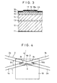
- Fig. 4 is a plan view showing an example of a switch according to the present invention.
- this switch differs from that of the total internal reflection-type optical waveguide switch of the conventional construction shown in Fig. 1 only in the configuration of the boundary surface between the refractive index changing region 4 and the remaining portions of the optical waveguides at the region of intersection.
- the boundary surface of the refractive index changing region 4 is shaped so that the portion thereof extending from an intersection A1 between incidence-side optical waveguides 1a and 2a to an intersection A2 between emission-side optical waveguides 1b and 2b has a concave which is recessed with respect to that lateral portion of the region of intersection 3 on the side of the incidence-side optical waveguide 2a (and emission-side optical waveguide 1b), as shown in Fig. 4.
- the concave may, for example, be a curved surface defined by a circular arc having a fixed curvature radius R or a curved surface defined by a curve with a gradually varying curvature radius, such as the circumference of an ellipse.
- the buffer layer 13 of e.g. n+GaAs, lower cladding layer 14 of e.g. n+AlGaAs, core layer 15 of e.g. n ⁇ GaAs, upper cladding layer 16 of e.g. n ⁇ AlGaAs, and cap layer 17 of e.g. n ⁇ GaAs are successively built up on the substrate 12 of n+GaAs by the MOCVD process.
- the configuration of the diffused region 4a includes the curved surface which is curved between the intersections A1 and A2 of Fig. 4 and defined by the circular arc having the curvature radius R.
- the masking material is removed, the cap layer 17 and the upper cladding layer 16 are etched so that the light to be guided is in a single mode, and the incidence-side optical waveguides la and 2a, the emission-side optical waveguides 1b and 2b, and the region of intersection 3 are formed each in the shape of a ridge so that the intersection angle is ⁇ .
- the insulating film 18 of e.g. SiO2 is formed on the whole surface of the resulting structure, the portion corresponding to the insulating film aperture 18a shown in Fig. 1 is removed by etching, and the upper electrode 19 of, e.g. Ti/Pt/Au, is mounted there. Finally, the lower surface of the GaAs substrate 12 is polished, and the lower electrode 11 of, e.g. AuGeNi/Au, is mounted thereon.
- the present invention is not limited to this, and the switch may alternatively be formed of a dielectric material, such as LiNbO3. If the material composition of the refractive index changing region is changed, moreover, switching operation can be performed by applying voltage from the upper electrode.
- the buffer layer 13 of n+GaAs 0.5 ⁇ m in thickness, lower cladding layer 14 of n+Al 0.2 Ga 0.8 As 3.0 ⁇ m in thickness, core layer 15 of n ⁇ GaAs 0.8 ⁇ m in thickness, upper cladding layer 16 of n ⁇ Al 0.2 Ga 0.8 As 0.8 ⁇ m in thickness, and cap layer 17 of n ⁇ GaAs 0.2 ⁇ m in thickness were successively built up on the n+GaAs substrate 12 by the MOCVD process.
- an optical switch such as the one shown in Fig. 4, was manufactured having the curvature radius R of 5 mm and the intersection angle ⁇ of 4° .
- Fig. 5 shows the switching characteristics of this optical waveguide switch for the light of 1.55 ⁇ m wavelength.
- a circle represents the emission power from the emission-side optical waveguide 2b obtained when the light is applied from the incidence-side optical waveguide 2a
- a black spot represents the emission power from the emission-side optical waveguide 1b.
- the initial crosstalk level of this optical switch is about 18.5 dB.
- this value indicates that the optical loss of the resulting optical switch is very small.
- An optical waveguide switch was manufactured in the same manner as Embodiment 1 except that the semiconductor compositions for the lower and upper cladding layers 14 and 16 were n+Al 0.1 Ga 0.9 As and n ⁇ Al 0.1 Ga 0.9 As, respectively, core layer 15 of n ⁇ GaAS was 1.0 ⁇ m in thickness, and that the intersection angle ⁇ was 5° .
- Fig. 6 shows the switching characteristics of this optical waveguide switch for the light of 1.55 ⁇ m wavelength.
- a circle represents the emission power from the emission-side optical waveguide 2b obtained when the light is applied from the incidence-side optical waveguide 2a, and a black spot represents the emission power from the emission-side optical waveguide 1b.
- this optical switch starts the switching operation at about 100 mA, and its initial crosstalk level is 16.0 dB.
- the operating crosstalk level of this optical switch is 17.8 dB.
- both the initial and operating crosstalk characteristics are highly improved.
- An optical waveguide switch was manufactured in the same manner as Embodiment 2 except that the intersection angle ⁇ was 6° .
- Fig. 7 shows the switching characteristics of this optical waveguide switch for the light of 1.55 ⁇ m wavelength.
- a circle represents the emission power from the emission-side optical waveguide 2b obtained when the light is applied from the incidence-side optical waveguide 2a
- a black spot represents the emission power from the emission-side optical waveguide 1b.
- this optical switch starts the switching operation at about 130 mA, and its initial crosstalk level is 18.7 dB.
- the operating crosstalk level of this optical switch is 9.9 dB.
- An optical waveguide switch was manufactured in the same manner as Embodiment 2 except that the crossing section 3 has a wide plane configuration having parallel lateral portions, as shown in Fig. 8.
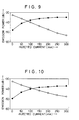
- Fig. 9 shows the switching characteristics of this optical waveguide switch for the light of 1.55 ⁇ m wavelength.
- a circle represents the emission power from the emission-side optical waveguide 2b obtained when the light is applied from the incidence-side optical waveguide 2a, and a black spot represents the emission power from the emission-side optical waveguide 1b.
- this optical switch starts the switching operation at about 80 mA, and its initial crosstalk level is 15.5 dB.
- the operating crosstalk level of this optical switch is 18.5 dB.
- both the initial and operating crosstalk characteristics are highly improved.
- An optical waveguide switch was manufactured in the same manner as Embodiment 4 except that the intersection angle ⁇ was 6° .
- Fig. 10 shows the switching characteristics of this optical waveguide switch for the light of 1.55 ⁇ m wavelength.
- a circle represents the emission power from the emission-side optical waveguide 2b obtained when the light is applied from the incidence-side optical waveguide 2a
- a black spot represents the emission power from the emission-side optical waveguide 1b.
- this optical switch starts the switching operation at about 110 mA, and its initial crosstalk level is 17.6 dB.
- the operating crosstalk level of this optical switch is 10.6 dB.
- An optical waveguide switch was manufactured in the same manner as Embodiment 2 except that each lateral portion the plane configuration of the region of intersection 3 was defined by the circumference of a circular arc with the curvature radius of 5 mm, and that the intersection angle ⁇ was 4° .
- the initial crosstalk level of this optical switch was 17.2 dB.
Landscapes
- Physics & Mathematics (AREA)
- Nonlinear Science (AREA)
- General Physics & Mathematics (AREA)
- Optics & Photonics (AREA)
- Optical Integrated Circuits (AREA)
Claims (5)
- Commutateur à guides d'ondes optiques du type à réflexion interne totale comprenant:
des guides d'ondes optiques (1,2) qui s'entrecroisent l'un l'autre et qui comportent, à l'intérieur de la région (3) d'intersection une surface de délimitation ayant une région (4) à index de réfraction modifiable, dans laquelle l'index de réfraction est différent par rapport aux portions restantes desdits guides d'ondes (1,2) pour réfléchir la lumière, caractérisé en ce que ladite surface de délimitation est concave. - Commutateur à guides d'ondes optiques du type à reflexion interne totale selon la revendication 1, dans lequel chacun desdits guides d'ondes optiques (1,2) est formé par un matériel semi-conducteur ou diélectrique.
- Commutateur à guides d'ondes optiques du type à reflexion interne totale selon la revendication 1, dans lequel ladite surface de délimitation concave est une surface courbe définie par un arc de cercle ou d'ellipse.
- Commutateur à guides d'ondes optiques du type à reflexion interne totale selon la revendication 1, dans lequel l'angle d'intersection entre lesdits guides d'ondes optiques (1,2) se situe dans un intervalle de 4° à 6°, tandis que la courbe qui définit ladite surface de délimitation concave est un arc circulaire, ayant un rayon de courbure de 5 mm.
- Commutateur à guides d'ondes optiques du type à reflexion interne totale selon la revendication 1, comprenant en outre des électrodes (11, 19) pour activer ladite région à index de réfraction modifiable par une injection de courant ou application de tension.
Applications Claiming Priority (2)
| Application Number | Priority Date | Filing Date | Title |
|---|---|---|---|
| JP265994/91 | 1991-10-15 | ||
| JP26599491 | 1991-10-15 |
Publications (2)
| Publication Number | Publication Date |
|---|---|
| EP0537703A1 EP0537703A1 (fr) | 1993-04-21 |
| EP0537703B1 true EP0537703B1 (fr) | 1996-03-20 |
Family
ID=17424893
Family Applications (1)
| Application Number | Title | Priority Date | Filing Date |
|---|---|---|---|
| EP92117535A Expired - Lifetime EP0537703B1 (fr) | 1991-10-15 | 1992-10-14 | Commutateur à guides d'ondes optiques du type à réflexion interne totale |
Country Status (4)
| Country | Link |
|---|---|
| US (1) | US5369718A (fr) |
| EP (1) | EP0537703B1 (fr) |
| CA (1) | CA2080563C (fr) |
| DE (1) | DE69209212T2 (fr) |
Families Citing this family (31)
| Publication number | Priority date | Publication date | Assignee | Title |
|---|---|---|---|---|
| US5771321A (en) * | 1996-01-04 | 1998-06-23 | Massachusetts Institute Of Technology | Micromechanical optical switch and flat panel display |
| US6768572B2 (en) | 1997-10-29 | 2004-07-27 | Teloptics Corporation | Solid state free space switch array on a substrate |
| US6816296B2 (en) | 1997-10-29 | 2004-11-09 | Teloptics Corporation | Optical switching network and network node and method of optical switching |
| US6310712B1 (en) | 1997-10-29 | 2001-10-30 | Teloptics Corporation | Discrete element light modulating microstructure devices |
| US6253007B1 (en) | 1998-07-08 | 2001-06-26 | Optical Switch Corporation | Method and apparatus for connecting optical fibers |
| US6137930A (en) * | 1998-07-08 | 2000-10-24 | Optical Switch Corporation | Method and apparatus for aligning optical fibers |
| US6236787B1 (en) | 1998-07-08 | 2001-05-22 | Optical Switch Corporation | Method and apparatus for aligning optical fibers using an alignment spacer |
| US6144780A (en) * | 1998-10-05 | 2000-11-07 | Lucent Technologies Inc. | Polymer waveguide switch and method |
| US6486996B1 (en) | 1998-10-27 | 2002-11-26 | Teloptics Corporations | Discrete element light modulating microstructure devices |
| US6236778B1 (en) | 1998-12-16 | 2001-05-22 | Optical Switch Corporation | Frustrated total internal reflection bus and method of operation |
| US6243511B1 (en) | 1999-02-04 | 2001-06-05 | Optical Switch Corporation | System and method for determining the condition of an optical signal |
| US6317531B1 (en) * | 1999-09-17 | 2001-11-13 | Agilent Technologies, Inc. | Optical cross-connect utilizing metal/hydride mirrors |
| US6438283B1 (en) | 1999-10-08 | 2002-08-20 | Optical Switch Corporation | Frustrated total internal reflection switch using double pass reflection and method of operation |
| US6519382B1 (en) | 2000-09-11 | 2003-02-11 | Optical Switch Corporation | Frustrated total internal reflection switch using waveguides and method of operation |
| US6529655B1 (en) | 2000-11-14 | 2003-03-04 | Optical Switch Corporation | Frustrated total internal reflection optical switch using waveguides and method of operation |
| US6516111B1 (en) | 2000-11-15 | 2003-02-04 | Optical Switch Corporation | Cascaded integrated fiber array optical switch and method of operation |
| US6516107B1 (en) | 2000-11-15 | 2003-02-04 | Optical Switch Corporation | 2×2 integrated fiber array optical switch and method of operation |
| US6393175B1 (en) | 2000-11-15 | 2002-05-21 | Optical Switch Corporation | Integrated fiber array optical switch and method of operation |
| US6393174B1 (en) | 2000-11-15 | 2002-05-21 | Optical Switch Corporation | Integrated fiber array optical switch using double-pass propagation and method of operation |
| US6529653B1 (en) | 2001-04-11 | 2003-03-04 | Optical Switch Corporation | System and method for orienting and positioning optical fibers |
| US6963441B2 (en) * | 2001-05-04 | 2005-11-08 | Teloptics, Corporation | Deactivated electro-optic material and method of forming the same |
| US6633692B2 (en) | 2001-07-31 | 2003-10-14 | The National University Of Singapore | High carrier injection optical waveguide switch |
| US6707958B2 (en) | 2001-11-20 | 2004-03-16 | Agilent Technologies, Inc. | Biochemical assay device using frustrated total internal reflection modulator with an imaging optical waveguide |
| GB2383425A (en) * | 2001-12-19 | 2003-06-25 | Bookham Technology Plc | Integrated optical device |
| US7447397B1 (en) * | 2004-06-14 | 2008-11-04 | Dynamic Method Enterprises Limited | Optical switch matrix |
| US7397989B2 (en) * | 2004-09-21 | 2008-07-08 | Dynamic Method Enterprises Limited | Optical switches |
| US8131124B2 (en) * | 2008-04-22 | 2012-03-06 | Jamshid Nayyer | Optical guided mode spatial switches and their fabrication |
| US8358901B2 (en) * | 2009-05-28 | 2013-01-22 | Microsoft Corporation | Optic having a cladding |
| US20120243826A1 (en) * | 2011-03-21 | 2012-09-27 | Liping Sun | Low power compact optical switch |
| DE102015122055B4 (de) * | 2015-12-17 | 2018-08-30 | Carl Zeiss Ag | Optisches System sowie Verfahren zum Übertragen eines Quellbildes |
| US10816871B1 (en) | 2017-07-31 | 2020-10-27 | Jamshid Nayyer | Fast spatial light switches and their fabrication |
Family Cites Families (12)
| Publication number | Priority date | Publication date | Assignee | Title |
|---|---|---|---|---|
| JPS5915225A (ja) * | 1982-07-15 | 1984-01-26 | Omron Tateisi Electronics Co | 光スイツチ |
| JPS5928132A (ja) * | 1982-08-09 | 1984-02-14 | Omron Tateisi Electronics Co | 光スイツチ |
| DE3482287D1 (de) * | 1983-02-10 | 1990-06-21 | Matsushita Electric Industrial Co Ltd | Optischer schalter. |
| JPH0685035B2 (ja) * | 1986-01-29 | 1994-10-26 | 株式会社日立製作所 | 光スイツチ |
| US4746183A (en) * | 1986-02-24 | 1988-05-24 | The United States Of America As Represented By The Secretary Of The Air Force | Electrically controlled integrated optical switch |
| JPS6310134A (ja) * | 1986-07-01 | 1988-01-16 | Oki Electric Ind Co Ltd | 導波型光スイツチ |
| JPH0721594B2 (ja) * | 1987-01-19 | 1995-03-08 | 国際電信電話株式会社 | 光スイツチ |
| US4775207A (en) * | 1987-03-17 | 1988-10-04 | Bell Communications Research, Inc. | Electro-optical switch |
| US5033811A (en) * | 1988-11-04 | 1991-07-23 | The Furukawa Electric Co., Ltd. | Optical switch |
| JPH02298923A (ja) * | 1989-05-12 | 1990-12-11 | Fujikura Ltd | 半導体光スイッチ |
| JPH0355525A (ja) * | 1989-07-25 | 1991-03-11 | Furukawa Electric Co Ltd:The | 導波路型光スイッチ |
| JP2788922B2 (ja) * | 1990-01-11 | 1998-08-20 | 日本電信電話株式会社 | 光競合制御回路 |
-
1992
- 1992-10-13 US US07/960,554 patent/US5369718A/en not_active Expired - Fee Related
- 1992-10-14 DE DE69209212T patent/DE69209212T2/de not_active Expired - Fee Related
- 1992-10-14 EP EP92117535A patent/EP0537703B1/fr not_active Expired - Lifetime
- 1992-10-14 CA CA002080563A patent/CA2080563C/fr not_active Expired - Fee Related
Also Published As
| Publication number | Publication date |
|---|---|
| DE69209212T2 (de) | 1996-10-31 |
| CA2080563C (fr) | 1999-12-21 |
| EP0537703A1 (fr) | 1993-04-21 |
| CA2080563A1 (fr) | 1993-04-16 |
| US5369718A (en) | 1994-11-29 |
| DE69209212D1 (de) | 1996-04-25 |
Similar Documents
| Publication | Publication Date | Title |
|---|---|---|
| US5369718A (en) | Total internal reflection-type optical waveguide switch | |
| EP0543369B1 (fr) | Modulateur de commutateur avec guides d'ondes antirésonnantes et réfléchissantes ("ARROWS") sur silicium | |
| US4773720A (en) | Optical waveguide | |
| KR910002028A (ko) | 반도체 장치 및 그 제조방법 | |
| EP0367682B1 (fr) | Commutateur optique | |
| US4245883A (en) | Electrochromic optical device | |
| US6210867B1 (en) | Method for fabricating low-loss optically active device | |
| US4589117A (en) | Butt-jointed built-in semiconductor laser | |
| US5255334A (en) | Directional coupler type optical device and a driving method therefor | |
| US6384955B2 (en) | Light modulator | |
| JP2792826B2 (ja) | 光スイッチおよびその製造方法 | |
| KR930009600B1 (ko) | 반도체 소자 | |
| JPH05210127A (ja) | 全反射型光導波路スイッチ | |
| JPH03278030A (ja) | 全反射型光導波路スイッチ | |
| JPH02298923A (ja) | 半導体光スイッチ | |
| JP2873303B2 (ja) | 半導体光導波路 | |
| KR950009631B1 (ko) | 내부전반사형 반도체 광 스위치소자 | |
| KR970004495B1 (ko) | 반도체 광스위치 제조방법 | |
| JPH04350628A (ja) | 導波路型光スイッチ | |
| KR970008342B1 (ko) | 이온 주입에 의한 고속 광스위치 제조방법 | |
| KR900006923B1 (ko) | 지붕형 반사기를 갖는 반도체 레이저 구조 | |
| JPS60222819A (ja) | 光集積回路およびその製作法 | |
| JPH0230195B2 (fr) | ||
| JPS63202722A (ja) | 光スイツチ | |
| JPH0355525A (ja) | 導波路型光スイッチ |
Legal Events
| Date | Code | Title | Description |
|---|---|---|---|
| PUAI | Public reference made under article 153(3) epc to a published international application that has entered the european phase |
Free format text: ORIGINAL CODE: 0009012 |
|
| AK | Designated contracting states |
Kind code of ref document: A1 Designated state(s): DE FR GB SE |
|
| 17P | Request for examination filed |
Effective date: 19931004 |
|
| 17Q | First examination report despatched |
Effective date: 19950518 |
|
| GRAA | (expected) grant |
Free format text: ORIGINAL CODE: 0009210 |
|
| AK | Designated contracting states |
Kind code of ref document: B1 Designated state(s): DE FR GB SE |
|
| PG25 | Lapsed in a contracting state [announced via postgrant information from national office to epo] |
Ref country code: FR Effective date: 19960320 |
|
| REF | Corresponds to: |
Ref document number: 69209212 Country of ref document: DE Date of ref document: 19960425 |
|
| PG25 | Lapsed in a contracting state [announced via postgrant information from national office to epo] |
Ref country code: SE Effective date: 19960620 |
|
| EN | Fr: translation not filed | ||
| PLBE | No opposition filed within time limit |
Free format text: ORIGINAL CODE: 0009261 |
|
| STAA | Information on the status of an ep patent application or granted ep patent |
Free format text: STATUS: NO OPPOSITION FILED WITHIN TIME LIMIT |
|
| 26N | No opposition filed | ||
| PGFP | Annual fee paid to national office [announced via postgrant information from national office to epo] |
Ref country code: GB Payment date: 19991013 Year of fee payment: 8 |
|
| PGFP | Annual fee paid to national office [announced via postgrant information from national office to epo] |
Ref country code: DE Payment date: 19991018 Year of fee payment: 8 |
|
| PG25 | Lapsed in a contracting state [announced via postgrant information from national office to epo] |
Ref country code: GB Free format text: LAPSE BECAUSE OF NON-PAYMENT OF DUE FEES Effective date: 20001014 |
|
| GBPC | Gb: european patent ceased through non-payment of renewal fee |
Effective date: 20001014 |
|
| PG25 | Lapsed in a contracting state [announced via postgrant information from national office to epo] |
Ref country code: DE Free format text: LAPSE BECAUSE OF NON-PAYMENT OF DUE FEES Effective date: 20010703 |