EP0539109A1 - Presspritzform mit Kompensationseinspritzkanal - Google Patents
Presspritzform mit Kompensationseinspritzkanal Download PDFInfo
- Publication number
- EP0539109A1 EP0539109A1 EP92309449A EP92309449A EP0539109A1 EP 0539109 A1 EP0539109 A1 EP 0539109A1 EP 92309449 A EP92309449 A EP 92309449A EP 92309449 A EP92309449 A EP 92309449A EP 0539109 A1 EP0539109 A1 EP 0539109A1
- Authority
- EP
- European Patent Office
- Prior art keywords
- mold
- molding compound
- mold cavities
- runners
- gate means
- Prior art date
- Legal status (The legal status is an assumption and is not a legal conclusion. Google has not performed a legal analysis and makes no representation as to the accuracy of the status listed.)
- Withdrawn
Links
Images



Classifications
-
- B—PERFORMING OPERATIONS; TRANSPORTING
- B29—WORKING OF PLASTICS; WORKING OF SUBSTANCES IN A PLASTIC STATE IN GENERAL
- B29C—SHAPING OR JOINING OF PLASTICS; SHAPING OF MATERIAL IN A PLASTIC STATE, NOT OTHERWISE PROVIDED FOR; AFTER-TREATMENT OF THE SHAPED PRODUCTS, e.g. REPAIRING
- B29C45/00—Injection moulding, i.e. forcing the required volume of moulding material through a nozzle into a closed mould; Apparatus therefor
- B29C45/17—Component parts, details or accessories; Auxiliary operations
- B29C45/26—Moulds
- B29C45/27—Sprue channels ; Runner channels or runner nozzles
- B29C45/2701—Details not specific to hot or cold runner channels
- B29C45/2703—Means for controlling the runner flow, e.g. runner switches, adjustable runners or gates
- B29C45/2704—Controlling the filling rates or the filling times of two or more mould cavities by controlling the cross section or the length of the runners or the gates
-
- B—PERFORMING OPERATIONS; TRANSPORTING
- B29—WORKING OF PLASTICS; WORKING OF SUBSTANCES IN A PLASTIC STATE IN GENERAL
- B29C—SHAPING OR JOINING OF PLASTICS; SHAPING OF MATERIAL IN A PLASTIC STATE, NOT OTHERWISE PROVIDED FOR; AFTER-TREATMENT OF THE SHAPED PRODUCTS, e.g. REPAIRING
- B29C45/00—Injection moulding, i.e. forcing the required volume of moulding material through a nozzle into a closed mould; Apparatus therefor
- B29C45/02—Transfer moulding, i.e. transferring the required volume of moulding material by a plunger from a "shot" cavity into a mould cavity
-
- H—ELECTRICITY
- H10—SEMICONDUCTOR DEVICES; ELECTRIC SOLID-STATE DEVICES NOT OTHERWISE PROVIDED FOR
- H10W—GENERIC PACKAGES, INTERCONNECTIONS, CONNECTORS OR OTHER CONSTRUCTIONAL DETAILS OF DEVICES COVERED BY CLASS H10
- H10W74/00—Encapsulations, e.g. protective coatings
- H10W74/01—Manufacture or treatment
- H10W74/016—Manufacture or treatment using moulds
-
- B—PERFORMING OPERATIONS; TRANSPORTING
- B29—WORKING OF PLASTICS; WORKING OF SUBSTANCES IN A PLASTIC STATE IN GENERAL
- B29C—SHAPING OR JOINING OF PLASTICS; SHAPING OF MATERIAL IN A PLASTIC STATE, NOT OTHERWISE PROVIDED FOR; AFTER-TREATMENT OF THE SHAPED PRODUCTS, e.g. REPAIRING
- B29C45/00—Injection moulding, i.e. forcing the required volume of moulding material through a nozzle into a closed mould; Apparatus therefor
- B29C45/17—Component parts, details or accessories; Auxiliary operations
- B29C45/26—Moulds
- B29C2045/2683—Plurality of independent mould cavities in a single mould
- B29C2045/2687—Plurality of independent mould cavities in a single mould controlling the filling thereof
-
- H—ELECTRICITY
- H10—SEMICONDUCTOR DEVICES; ELECTRIC SOLID-STATE DEVICES NOT OTHERWISE PROVIDED FOR
- H10W—GENERIC PACKAGES, INTERCONNECTIONS, CONNECTORS OR OTHER CONSTRUCTIONAL DETAILS OF DEVICES COVERED BY CLASS H10
- H10W72/00—Interconnections or connectors in packages
- H10W72/851—Dispositions of multiple connectors or interconnections
- H10W72/874—On different surfaces
- H10W72/884—Die-attach connectors and bond wires
Definitions
- This invention relates to molds for encapsulating an integrated semiconductor device coupled to a leadframe by the transfer molding process and more particularly to an improved runner design for a multicavity mold which equalizes the viscosity of the molding compound flowing into each mold cavity.
- plastic molding compounds are used to encapsulate a very large percentage of the multitude of silicon-integrated devices packaged throughout the world each year.
- the concept of encapsulating one or more silicon devices within a plastic package has contributed materially to reducing the cost of packaging devices. This, in turn, has led to the use of silicon devices in a wide array of products.
- the development of molding compounds which exhibit low thermal coefficients of expansion and high fracture toughness has enabled transfer molding to be used in high volume production to package or encapsulate silicon integrated devices.
- the transfer molding process can be thought of as being comprised of the three distinct phases of A) filling a multicavity mold with molding compound, B) packing the molding compound in the mold, and C) curing the molding compound.
- This invention is directed toward increasing the yield of encapsulated silicon integrated devices.
- the present invention is directed toward a multicavity mold which provides a more balanced fill profile by equalizing the viscosity of the material which enters each cavity.
- the result is a reduced number of rejects caused by the molding process, and a finished product which can withstand relatively high temperature, is rugged in nature, and is compatible with modem high-speed pick and place technologies.
- Silicon integrated devices because of their small size and fragile nature are frequently embedded in a plastic molding compound and electrically connected to an array of electrical conductors which project beyond the edge of the assemblage.
- the ends of the electrical conductors embedded within the plastic molding compound and located close to the silicon device are known as the inner leads and are connected to bonding pads on the silicon device through fine wire bonds.
- the outer ends of the leads which project outward from the edge of the assemblage are shaped to form "J" type leads or "gull wing" leads for mounting onto a circuit board.
- the plurality of leads which connect the silicon device to the circuit board is stamped or punched from sheet material and is called a leadframe .
- the leads may be formed by etching because the spacing between the inner leads may be too small to be formed with a punch tool.
- each lead is connected to a bond pad on a silica device by means of a gold or aluminum wire.
- the silicon devices are supported by a ceramic member which, in turn, is physically supported by the inner leads.
- the ends of the inner leads are electrically connected to the silicon device and also provides support for the silicon device.
- One method of forming the final package is by a "post-molding" process.
- the leadframe and the attached silicon integrated device is encapsulated by a thermoset plastic molding compound.
- Encapsulation normally occurs in a production-size molding tool over a three minute cycle. Of the three minute cycle time, the plastic molding compound flows into the mold in about 15 seconds, two minutes is needed to polymerize or cure the plastic; and the remaining time is used to prepare the mold for the next molding cycle, The plastic molding compound generates flow-induced stresses on the fragile silicon device, the connecting wires and the leads as it fills the cavity. This flow-induced stress causes damage and yield loss.
- a silicon device 10 is secured to a ceramic member 12 by thermally conductive epoxy adhesive 14.
- the ceramic member 12 supports conductive paths for making electrical connections from the silicon device to the leads of a lead frame 24.
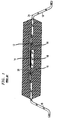
- Fig. 2 illustrates a typical leadframe 24.
- fine wire bonds 16 electrically connect the various bond pads on the silicon device 10 to appropriate conductive paths on the ceramic member 12.
- the conductive paths on the ceramic member 12 are also connected electrically to the inner ends of the various leads 18 of the leadframe 24.
- the ceramic member 12, silicon device 10, wire bonds 16 and inner ends of the leads 18 are embedded within plastic molding compound 20 which provides support and electrical isolation.
- the lead 18 for surface mount packages are normally formed into "J" leads or "gull wing” leads.
- J leads extend under the molded body and conserve area on the circuit board. However, they are difficult to inspect.
- Gull wing leads, such as leads 18 are formed to extend away from the molded body and allow for visual inspection of solder attachments to a printed circuit board. Fine pitch plastic packages typically use gull wing lead when attachment yield is an issue.
- the leadframe 24 can be of a flat sheet of metal such as copper, copper alloy or the like stamped or etched to form a square on a rectangle of a plurality of conductive leads 18 having inner ends 26 and outer ends 28.
- the outer ends 28 are attached to an outer frame support member 30 which holds the various leads 18 in position relative to each other until after the ends 26 of the leads 18 have been connected to the ceramic member 12 and the wire bands 16, and the assemblage has been encapsulated in the plastic molding compound. Following the molding process the outer frame support member 30 is removed from the leads 18; and, the ends 28 of the leads 18 are formed to the final configuration in a trim and form operation.
- microelectronic devices there are several different organic and inorganic materials used to package silicon devices commonly referred to as microelectronic devices. They include copper-rich alloys and an iron-nickel alloy. Iron-nickel has a coefficient of thermal expansion which is closer to silicon and has better mechanical properties than the copper-based alloys. The disadvantage of iron-nickel is that it has a low thermal conductivity. The ever increasing need to dissipate heat as the devices become larger requires using copper alloys, it being remembered, however, that these materials have limitations on thermal expansion and mechanical properties.
- the metal leads 18 have a direct effect on the performance characteristics of the device as they provide a path for removing heat from the silicon device.
- the leads are formed from punched or stamped sheet stock. Those which require high interconnection density, such as 164-lead packages and above, are normally formed by etching because the inner lead spacing is too small to be formed with a punching tool.
- Gold or aluminum wires 12 are used to connect the ends 26 of the leads to the band pads on the silicon device.
- the encapsulating material which is a thermoset polymer molding compound, is one of the most important materials in molded plastic packaging.
- the molding polymer is converted from a low-viscosity fluid to a hard plastic during the process. Although it has a softening point, or glass transition temperature, it does not flow after polymerization, even at soldering temperatures, because it has a cross-linked molecular architecture.
- Epoxy is the cross-linkable resin for nearly all commercial molding compounds.
- the formulation consists of a mixture of epoxy resin, hardener, catalyst, fillers, flame retardants, flexiblizers, coupling agents, mold release agents and colorants.
- Important molding compound properties include low viscosity to reduce damage to the fragile assemblies during molding, rapid cure to provide high productivity and low thermal shrinkage forces caused by differences in coefficient of thermal expansion among molding compound, leadframe and the silicon device.
- the molding compound contains about 75 percent by weight of inorganic filler, e.g., ground silicon to lower the coefficient of thermal expansion and increase thermal conductivity. Higher filler loadings achieved trough improvements in filler size and size distribution have lowered the coefficient of thermal expansion while reducing the material viscosity.
- inorganic filler e.g., ground silicon
- thermoset molding compounds Almost all post-molded plastic packages are made by the transfer molding process using thermoset molding compounds.
- an assembled leadframe is loaded on the molding tool either manually or with an automated leadframe loader and the molding tool is then placed in an oven where it is preheated.
- the molding compound is pre-softened by heating it in a dielectric preheater above its glass transition temperature. It is then placed in a cylindrical cavity in the molding tool.
- the operator starts the transfer by beginning the plunger movement that pushes the molding compound out of the transfer pot and into either the top or bottom portion of the preheated mold cavity.
- the pressure is increased to pack and further polymerized the molding compound under a higher applied pressure. Packing is important because the material is porous after filling. Packing compresses both macroscopic and microscopic voids in the molded body and lowers package permeability to eliminate voids where water can collect and promote corrosion. After the molding process, the leads are formed.
- the flow of the molding material and its subsequent properties after molding are a function of the process profile, i.e., pressure, temperature, velocity, time; the deformation and flow characteristics of the molding material, and the features and geometrics of the mold.
- the transfer molding process can be considered to be comprised of three distinct phases identified as filling, packing, and curing.
- the types of defects which commonly occur during molding include incomplete fills, voids - air bubbles from incomplete venting; blisters - air bubbles remaining at the surface; pinholes - voids which are open at the surface; and various forms of internal device damage.
- the last noted category can include one or more of the following: A) Wire sweep which is caused by flow-induced stress due to viscous drag and surface tension effects; B) Leadframe and/or wire damage due to excessive molding pressure or material forces in individual cavities of a multicavity mold; and C) Molding compound pressure imbalance above and below the leadframe causing excessive bending and tensile stresses in the wires and other components.
- the first step in the molding of a thermoset is to heat both the mold assemblage and the material.
- the material is heated to its softening point, normally with a dielectric heater.
- the softening temperature is near 90 ° C for epoxy resins.
- the preheated molding material is then put into the transfer pot, and upon activation of the transfer cycle, a plunger moves downward and delivers the material through runners in the upper platen to the mold cavity.
- the material enters the mold and then travels through the runner system in a way that distributes the material to all of the cavities of the mold.
- the material enters each mold cavity through a narrow opening called a gate and air escapes from the mold cavities through small vents.
- Thermoset molding is characterized by the fact that the mold is heated to a temperature which is much higher than the temperature of the incoming material. Thus, the temperature of the molding material rises as it flows through the runner system. The amount of heat transferred to the molding compound, and thus the temperature of the molding compound is dominated by conduction and frictional heating of the molding compound as it advances along the runners of the mold, Thus, as the molding material traveling through the runners, its temperature increases and thus its viscosity is changed.
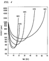
- the viscosity of the heated material goes through a minimum and begins to increase as the material cures.
- the precise viscosity vs. time curve depends principally on the temperature and shear rate of the material.
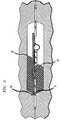
- the molding material enters the cavity from a runner 30 and gate 31 located above the leadframe, splits into two parts, a top part 32 being above the leadframe and a lower part 33 being below the leadframe.
- Each part advances simultaneously above and below the leadframe as is illustrated in Fig. 3.
- the fronts of each part advance at different rates based on cavity thicknesses and process conditions.
- the location where the flow fronts meet is called a weld or nit line.
- the weld line is an area of local weakness and can act as a stress concentration.
- the properties of the weld line will be proportional to the pressures and temperatures of the converging flow fronts.
- Epoxy novolac resins are the materials widely used for packaging microelectronic devices.
- the material is highly filled in order to lower its coefficient of expansion to be compatible with leadframe materials and other components to be encapsulated.
- the formulation of the material can include, in various amounts, the following ingredients: Epoxy novolac, Phenal novolac, catalyst, low stress additive, Releasing agent, Filler, and Black carbon.
- epoxies used in transfer molding are extremely complex in nature.
- epoxies are non-Newtonian time-dependent fluids, where the shear rate is proportional to the magnitude and duration of shear stress.
- the material is thixotropic and exhibits a reversible decrease in shear stress with time at a constant shear rate and temperature.
- a hysteresis occurs where shear stress does not follow the same path.
- Fig. 4 shows viscosity data for common molding compounds as a function of shear rate, temperature, and time.
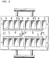
- FIG. 5 there is a view of a prior art top plate mold assembly illustrating the runners and mold cavities.
- the runner system is the standard H configuration where the material coming from the pot travels to port 50 of runner 52, then along runners 53 and 54 to fill the eight cavities 56, 58, 60, 62, 64, 66, 68, 70. The runners are filled from port 50 of runner 52 outward.
- Fig. 6 shows a typical part with a bowed leadframe where standard and recommended process parameters were used.
- Fig. 7 illustrates typical prior art hydraulic pressure Vs. time curve used to correct the bowing problem.
- the packing pressure is ramped down immediately after 100-percent fill to a low level. This reduction of pressure allows the parts to be filled and minimally packed for use as engineering models, but dots not provide for optimum processing conditions to maximize yield and reliability.
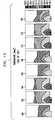
- Fig. 8 shows one increment of the filling profile. The material enters and substantially fills the center cavities first. Thereafter, the outside cavities begin to fill. Later on, the inside cavities slow in fill velocity as the outside cavities actually speed up and pass the inside cavities.
- the material in the center cavities appears to slow in velocity and may even hesitate.
- the flow from the pot is then directed towards the outside cavities, where the flow fronts pass the flow fronts in the inner cavities.
- This transient effect is really an equilibrium condition where the material tends to flow in the direction of the least resistance.
- FIG. 9 there is illustrated temperature contours at 60-percent fill.
- the material enters the platen of the mold at 100 ° C and reaches 104.4 ° when it exits the feed runner.
- the material is a thermoset
- its properties at the completion of the molding process are affected by its time and temperature histories. In this case, it can be observed that there is a large temperature and time difference between fill profiles between the inside and outside cavities. This causes the properties of the packages being molded in the inside and outside cavities to be different.
- Fig. 10 illustrates a runner system in accordance with the principles of the invention for balancing the temperature of molding material flowing into the eight mold cavities along one side of a transfer mold.
- a longer runner length provides for more heat transfer into the molding material which enters each gate. This results not only in lower viscosity, but a more uniform viscosity of the molding material flowing into each mold cavity.
- a view of a top plate of a transfer mold die having sixteen mold cavities 100-130 there is illustrated a view of a top plate of a transfer mold die having sixteen mold cavities 100-130.
- the transfer die mold can be considered to be comprised of four sections, each comprised of four similar size mold cavities. Section one includes mold cavities 100-106; section two includes mold cavities 108-114; section three includes mold cavities 116-122; and, section four includes mold cavities 124-130. Referring to the section one which consists of mold cavities 100-106; each mold cavity 100-106 is connected, via similar sized gates 101-107 and a balanced runner array 134, to a molding compound entry port 132.
- the balanced runner array 134 comprises a plurality of runners which extend from entry port 132 to each gate 101 - 107 where each runner is sized to deliver to each gate 101-107 of each die cavity 100-106 molding compound having substantially similar temperatures.
- One such arrangement is illustrated in Fig. 10 where the distances between the molding compound entry port 132 and the gates 101-107 of the die cavities 100-106 are substantially equal.
- the die cavities of the other sections are coupled to receive molding compound from entry port 132 via a similar runner array.
- the various arms 136, 138 and 140 of the runner array art sized to prevent the occurrence of molding compound starvation in any arm.
- FIG. 11 there is illustrated the flow of molding compound into eight mold cavities using the new improved runner system here disclosed.
- Fig. 12 illustrates a typical pressure versus time profile for the new improved runner here disclosed. Clearly, the fill profile is more desirable. The resulting parts reflected much better packing and eliminated the bowing problem.
- Fig. 13 shows temperature profiles at 60-percent fill.
- the maximum difference in molding compound temperatures is 8.1 °C, which is half of what it was in the prior art mold. This smaller temperature differential is a key factor in equalizing the viscosity of the material in each cavity and providing for a mort balanced fill profile.
Landscapes
- Engineering & Computer Science (AREA)
- Manufacturing & Machinery (AREA)
- Mechanical Engineering (AREA)
- Moulds For Moulding Plastics Or The Like (AREA)
- Injection Moulding Of Plastics Or The Like (AREA)
- Encapsulation Of And Coatings For Semiconductor Or Solid State Devices (AREA)
Applications Claiming Priority (2)
| Application Number | Priority Date | Filing Date | Title |
|---|---|---|---|
| US78204291A | 1991-10-24 | 1991-10-24 | |
| US782042 | 1991-10-24 |
Publications (1)
| Publication Number | Publication Date |
|---|---|
| EP0539109A1 true EP0539109A1 (de) | 1993-04-28 |
Family
ID=25124770
Family Applications (1)
| Application Number | Title | Priority Date | Filing Date |
|---|---|---|---|
| EP92309449A Withdrawn EP0539109A1 (de) | 1991-10-24 | 1992-10-16 | Presspritzform mit Kompensationseinspritzkanal |
Country Status (4)
| Country | Link |
|---|---|
| EP (1) | EP0539109A1 (de) |
| JP (1) | JPH06285898A (de) |
| KR (1) | KR960007277B1 (de) |
| TW (1) | TW208759B (de) |
Cited By (7)
| Publication number | Priority date | Publication date | Assignee | Title |
|---|---|---|---|---|
| US5792409A (en) * | 1995-12-28 | 1998-08-11 | Gb Electrical, Inc. | Balanced multi-cavity injection molding of cable ties |
| EP0787569A3 (de) * | 1996-01-31 | 1999-04-21 | Sumitomo Bakelite Company Limited | Verfahren zur Herstellung von in Epoxyharz eingekapselter Halbleitervorrichtung |
| EP0909628A3 (de) * | 1997-09-16 | 2002-03-27 | K.K. Holding Ag | Verfahren zur Regelung der Heisskanalheizung eines Mehrkavitäten-Spritzgiesswerkzeugs |
| EP1864780A3 (de) * | 2006-06-09 | 2008-02-20 | LG Electronics Inc. | Lichtemittierende Einheit, Herstellungsvorrichtung und Verfahren dafür, Vorrichtung zum Formen einer Linse dafür und Verpackung für die lichtemittierende Vorrichtung |
| CN102343650A (zh) * | 2010-07-30 | 2012-02-08 | 株式会社东芝 | 浇铸模具和气体绝缘开关装置 |
| CN108987292A (zh) * | 2017-06-05 | 2018-12-11 | 日月光半导体制造股份有限公司 | 封装模具和半导体封装制程 |
| CN115503192A (zh) * | 2022-09-26 | 2022-12-23 | 株洲时代新材料科技股份有限公司 | 一种叠层橡胶-金属弹性轴承的梯度注胶成型方法及装置 |
Families Citing this family (2)
| Publication number | Priority date | Publication date | Assignee | Title |
|---|---|---|---|---|
| JP5050913B2 (ja) * | 2008-02-22 | 2012-10-17 | 株式会社デンソー | モールドパッケージの製造方法 |
| JP2010111014A (ja) * | 2008-11-06 | 2010-05-20 | Suzuki Motor Corp | 成形用金型及び成形品の製造方法 |
Citations (1)
| Publication number | Priority date | Publication date | Assignee | Title |
|---|---|---|---|---|
| US4620958A (en) * | 1984-09-28 | 1986-11-04 | At&T Technologies, Inc. | Methods of and apparatus for molding articles through a balanced, removable runner system |
-
1992
- 1992-07-02 TW TW081105253A patent/TW208759B/zh active
- 1992-10-16 EP EP92309449A patent/EP0539109A1/de not_active Withdrawn
- 1992-10-20 JP JP4306227A patent/JPH06285898A/ja active Pending
- 1992-10-23 KR KR1019920019572A patent/KR960007277B1/ko not_active Expired - Lifetime
Patent Citations (1)
| Publication number | Priority date | Publication date | Assignee | Title |
|---|---|---|---|---|
| US4620958A (en) * | 1984-09-28 | 1986-11-04 | At&T Technologies, Inc. | Methods of and apparatus for molding articles through a balanced, removable runner system |
Non-Patent Citations (4)
| Title |
|---|
| PATENT ABSTRACTS OF JAPAN vol. 10, no. 27 (E-378)(2084) 4 February 1986 & JP-A-60 187 031 ( FUJITSU K.K. ) * |
| PATENT ABSTRACTS OF JAPAN vol. 5, no. 105 (M-77)(777) 8 July 1981 & JP-A-56 049 208 ( HITACHI SEISAKUSHO K.K. ) * |
| PATENT ABSTRACTS OF JAPAN vol. 6, no. 69 (M-125)(947) 30 April 1982 & JP-A-57 008 138 ( TOKYO SHIBAURA DENKI KAISHA KABUSHIKI ) * |
| PATENT ABSTRACTS OF JAPAN vol. 7, no. 187 (M-236)(1332) 16 August 1983 & JP-A-58 089 346 ( HITACHI SEISAKUSHO K.K. ) * |
Cited By (16)
| Publication number | Priority date | Publication date | Assignee | Title |
|---|---|---|---|---|
| US5792409A (en) * | 1995-12-28 | 1998-08-11 | Gb Electrical, Inc. | Balanced multi-cavity injection molding of cable ties |
| EP0787569A3 (de) * | 1996-01-31 | 1999-04-21 | Sumitomo Bakelite Company Limited | Verfahren zur Herstellung von in Epoxyharz eingekapselter Halbleitervorrichtung |
| EP0985513A3 (de) * | 1996-01-31 | 2000-03-22 | Sumitomo Bakelite Company Limited | Verfahren zur Herstellung von in Epoxyharz eingekapselter Halbleitervorrichtung |
| SG91806A1 (en) * | 1996-01-31 | 2002-10-15 | Sumitomo Bakelite Co | Method of producing epoxy resin-encapsulated semiconductor device |
| EP0909628A3 (de) * | 1997-09-16 | 2002-03-27 | K.K. Holding Ag | Verfahren zur Regelung der Heisskanalheizung eines Mehrkavitäten-Spritzgiesswerkzeugs |
| CN101085543B (zh) * | 2006-06-09 | 2013-01-23 | Lg电子株式会社 | 发光单元及其制造设备和方法、用于模塑其透镜的设备和其发光器件封装 |
| EP1864780A3 (de) * | 2006-06-09 | 2008-02-20 | LG Electronics Inc. | Lichtemittierende Einheit, Herstellungsvorrichtung und Verfahren dafür, Vorrichtung zum Formen einer Linse dafür und Verpackung für die lichtemittierende Vorrichtung |
| US7496270B2 (en) | 2006-06-09 | 2009-02-24 | Lg Electronics Inc. | Light emitting unit, apparatus and method for manufacturing the same, apparatus for molding lens thereof, and light emitting device package thereof |
| US7869674B2 (en) | 2006-06-09 | 2011-01-11 | Lg Electronics Inc. | Light emitting unit, apparatus and method for manufacturing the same, apparatus for molding lens thereof, and light emitting device package thereof |
| CN102343650A (zh) * | 2010-07-30 | 2012-02-08 | 株式会社东芝 | 浇铸模具和气体绝缘开关装置 |
| EP2540468A1 (de) * | 2010-07-30 | 2013-01-02 | Kabushiki Kaisha Toshiba | Spritzgussform |
| EP2412504A3 (de) * | 2010-07-30 | 2012-03-28 | Kabushiki Kaisha Toshiba | Gussform und gasisoliertes Schaltgetriebe |
| CN102343650B (zh) * | 2010-07-30 | 2014-09-03 | 株式会社东芝 | 浇铸模具和气体绝缘开关装置 |
| CN108987292A (zh) * | 2017-06-05 | 2018-12-11 | 日月光半导体制造股份有限公司 | 封装模具和半导体封装制程 |
| CN115503192A (zh) * | 2022-09-26 | 2022-12-23 | 株洲时代新材料科技股份有限公司 | 一种叠层橡胶-金属弹性轴承的梯度注胶成型方法及装置 |
| CN115503192B (zh) * | 2022-09-26 | 2024-05-07 | 株洲时代新材料科技股份有限公司 | 一种叠层橡胶-金属弹性轴承的梯度注胶成型方法及装置 |
Also Published As
| Publication number | Publication date |
|---|---|
| KR960007277B1 (ko) | 1996-05-30 |
| JPH06285898A (ja) | 1994-10-11 |
| KR930007610A (ko) | 1993-05-20 |
| TW208759B (de) | 1993-07-01 |
Similar Documents
| Publication | Publication Date | Title |
|---|---|---|
| US5331205A (en) | Molded plastic package with wire protection | |
| US5197183A (en) | Modified lead frame for reducing wire wash in transfer molding of IC packages | |
| US5539251A (en) | Tie bar over chip lead frame design | |
| KR100753749B1 (ko) | 반도체 집적 회로 장치 및 그 제조 방법 | |
| US5213748A (en) | Method of molding a thermoplastic ring onto a leadframe | |
| US5256598A (en) | Shrink accommodating lead frame | |
| EP0515094A1 (de) | Gegossene Schaltungspackung | |
| US6657288B2 (en) | Compression layer on the lead frame to reduce stress defects | |
| US6083777A (en) | Reduced stress LOC assembly | |
| US6277225B1 (en) | Stress reduction feature for LOC lead frame | |
| EP0539109A1 (de) | Presspritzform mit Kompensationseinspritzkanal | |
| JP4039298B2 (ja) | 樹脂封止型半導体装置およびその製造方法ならびに成形型 | |
| EP0539108A1 (de) | Mehrfachnutzenpresspritzform mit viskositätskontrollierendem Einspritzkanal | |
| US5759875A (en) | Reduced filler particle size encapsulant for reduction in die surface damage in LOC packages and method of use | |
| JP3550100B2 (ja) | 自動車用電子回路装置及びそのパッケージ製造方法 | |
| JPH10270481A (ja) | 放射形ランナーを持つ半導体成形金型 | |
| JP2555931B2 (ja) | 半導体装置の製造方法 | |
| EP4379781A1 (de) | Verfahren zur herstellung von halbleiterbauelementen und zugehöriges halbleiterbauelement | |
| JP2828749B2 (ja) | リードフレーム | |
| KR19980030031A (ko) | 반도체 패키지용 금형 구조 | |
| KR19990012316A (ko) | 반도체 패키지의 몰딩 금형 장치 | |
| JPH07186187A (ja) | 順次進行する複数のチャネルを有する加熱移送モールド | |
| JPH0684987A (ja) | 半導体装置の樹脂封止金型及び製造方法 | |
| JPH08116001A (ja) | 半導体装置 |
Legal Events
| Date | Code | Title | Description |
|---|---|---|---|
| PUAI | Public reference made under article 153(3) epc to a published international application that has entered the european phase |
Free format text: ORIGINAL CODE: 0009012 |
|
| AK | Designated contracting states |
Kind code of ref document: A1 Designated state(s): DE FR GB NL |
|
| 17P | Request for examination filed |
Effective date: 19931018 |
|
| RAP3 | Party data changed (applicant data changed or rights of an application transferred) |
Owner name: AT&T CORP. |
|
| 17Q | First examination report despatched |
Effective date: 19940920 |
|
| 18D | Application deemed to be withdrawn |
Effective date: 19950331 |