EP0540946A2 - Verfahren zur digitalen Nachrichtenübertragung - Google Patents
Verfahren zur digitalen Nachrichtenübertragung Download PDFInfo
- Publication number
- EP0540946A2 EP0540946A2 EP92118055A EP92118055A EP0540946A2 EP 0540946 A2 EP0540946 A2 EP 0540946A2 EP 92118055 A EP92118055 A EP 92118055A EP 92118055 A EP92118055 A EP 92118055A EP 0540946 A2 EP0540946 A2 EP 0540946A2
- Authority
- EP
- European Patent Office
- Prior art keywords
- control unit
- decision maker
- summing point
- phase shifter
- signals
- Prior art date
- Legal status (The legal status is an assumption and is not a legal conclusion. Google has not performed a legal analysis and makes no representation as to the accuracy of the status listed.)
- Granted
Links
- 230000005540 biological transmission Effects 0.000 title claims abstract description 26
- 238000000034 method Methods 0.000 title claims abstract description 18
- 238000005070 sampling Methods 0.000 claims abstract description 13
- 238000011084 recovery Methods 0.000 claims abstract description 8
- 238000009751 slip forming Methods 0.000 claims abstract 2
- 239000004020 conductor Substances 0.000 claims description 3
- 230000006978 adaptation Effects 0.000 description 2
- 230000003287 optical effect Effects 0.000 description 2
- 230000003044 adaptive effect Effects 0.000 description 1
- 238000003491 array Methods 0.000 description 1
- 230000000712 assembly Effects 0.000 description 1
- 238000000429 assembly Methods 0.000 description 1
- 230000015572 biosynthetic process Effects 0.000 description 1
- 238000013461 design Methods 0.000 description 1
- 238000011156 evaluation Methods 0.000 description 1
- 230000006870 function Effects 0.000 description 1
- 238000004519 manufacturing process Methods 0.000 description 1
- 230000015654 memory Effects 0.000 description 1
- 238000012545 processing Methods 0.000 description 1
- 230000008054 signal transmission Effects 0.000 description 1
- 230000006641 stabilisation Effects 0.000 description 1
- 238000011105 stabilization Methods 0.000 description 1
- 230000002123 temporal effect Effects 0.000 description 1
- 230000036962 time dependent Effects 0.000 description 1
- 238000012546 transfer Methods 0.000 description 1
Images

Classifications
-
- H—ELECTRICITY
- H04—ELECTRIC COMMUNICATION TECHNIQUE
- H04L—TRANSMISSION OF DIGITAL INFORMATION, e.g. TELEGRAPHIC COMMUNICATION
- H04L7/00—Arrangements for synchronising receiver with transmitter
- H04L7/0054—Detection of the synchronisation error by features other than the received signal transition
- H04L7/0062—Detection of the synchronisation error by features other than the received signal transition detection of error based on data decision error, e.g. Mueller type detection
-
- H—ELECTRICITY
- H04—ELECTRIC COMMUNICATION TECHNIQUE
- H04L—TRANSMISSION OF DIGITAL INFORMATION, e.g. TELEGRAPHIC COMMUNICATION
- H04L7/00—Arrangements for synchronising receiver with transmitter
- H04L7/0079—Receiver details
- H04L7/0083—Receiver details taking measures against momentary loss of synchronisation, e.g. inhibiting the synchronisation, using idle words or using redundant clocks
Definitions
- the invention relates to a method for digital message transmission, in which the transmitted signals at the end of the transmission path are sampled by means of a clock recovery device and then further processed and fed to a decision maker (US-Z "IEEE TRANSACTIONS ON COMMUNICATIONS", VOL. COM-35 , NO. 9, September 1987, pages 961 to 968).
- signals via message transmission can be transmitted wired or wirelessly.
- Cables with electrical or optical transmission paths are used for wired transmission.
- the wireless transmission takes place, for example, via radio relay or satellite radio. Varying the transmission function of the transmission channel, for example by changing the length of a cable with metallic conductors, not only changes the shape of the signals received (pulses), but also shifts the temporal position of the respective pulse maximum.
- the entire pulse formation is also influenced by the temperature drift and the tolerances of the components or the cable used in the transmitter and receiver. It is therefore time-dependent and subject to a certain spread. In synchronously operated transmission systems combined in one cable, cyclical stationary faults continue to occur, the performance of which fluctuates periodically over time.
- the time of sampling or the clock phase are generally compared once during the manufacture of the respective assemblies. This means not only additional adjustment work, but the influencing factors described above are only insufficiently or not at all taken into account.
- the invention is based on the object of developing the method described at the outset in such a way that compliance with a permissible bit error rate is ensured and the range of the transmission can be increased.
- a phase shifter is therefore used, which is controlled by a control unit, for example a microcontroller.
- the control unit is supplied with the difference values between the signals at the input of the decision maker on the one hand and at the output thereof on the other hand from the summing point.
- the control unit forms an average value from the difference values supplied to it - for example the quadratic mean value or the mean value value - and after stabilization of the same - adjusts the phase shifter by a predeterminable amount. It is decisive for the point in time of an adjustment of the phase shifter that the system is in the steady state again after an adjustment, so that a stable mean value of the difference values is given.
- the sampling time is therefore constantly adapted to the respective circumstances.
- the method according to the invention can be used both in line-based message transmission via electrical or optical cables and in wireless message transmission.
- the method is of particular importance in the transmission of messages via electrical cables in which symmetrical double cores are combined with metallic conductors.
- the electrical cable is considered as the transmission medium.
- the distorted digital signals superimposed by interference travel from a cable 1 to a receiver 2, which has a reception filter 3, a scanning device 4 and a detector 5.
- a receiver 2 which has a reception filter 3, a scanning device 4 and a detector 5.
- FIG. 2 The more precise design of the receiver 2 is shown in FIG. 2:
- a phase shifter 8 connected to a clock recovery device 7 acts on the A / D converter 6.
- the decision-maker 10 recovers the source signals originally sent from the processed signals supplied by the filter unit 9.
- the input signal ES and output signal AS of the decision maker 10 are fed to a summing point 11.
- the output signal AS of the decision maker 10 can also be given to the filter unit 9 for evaluation.
- the difference signal D generated at the summing point 11 is applied to a control unit 12, which in turn controls the phase shifter 8.
- the amount ⁇ by which the phase shifter 8 is adjusted in each case is to be adapted to the circumstances. It should not be too small, so that the adaptation of the optimal sampling time does not take too long. On the other hand, an excessively large amount .DELTA..phi. Is not sensible, since the adaptation may then constantly oscillate back and forth and the optimum u. U. is not reached.
- the amount ⁇ by which the phase shifter 8 is adjusted remains the same in each case.
- a reasonable amount for ⁇ is, for example, 1% of the total clock phase.
- the amount ⁇ can also be variable. This can be useful if larger deviations occur.
- a further adjustment of the phase shifter 8 can be carried out by the same amount as before.
- the new stable mean M (i) is first compared to the previous stable mean M (i - 1) used for adjusting the phase shifter 8. If the new mean M (i) is smaller than the previous one, then the phase of the sampling time was shifted in the correct direction by the amount ⁇ . The next adjustment by the amount ⁇ then takes place in the same direction. If, on the other hand, the new mean M (i) is greater than the previous one, the phase is adjusted in the opposite direction by the amount ⁇ .
- the time of the adjustment can also be specified by the control unit 12. In any case, an adjustment is only made when the system has settled and the respective mean M (i) is stable. Accordingly, there is a pause between two adjustments of the sampling time.
- the filter unit 9 preferably consists of digital filters. Such filters are described, for example, in the DE-Z "FREQUENCY" mentioned at the beginning.
- the decision maker 10 can be a component known in the art of message transmission, such as a comparator or a logic circuit.
- the control unit 12 can be an intelligent module with memories, for example a microprocessor or a microcontroller. However, gate arrays or other logic circuits can also be used.
Landscapes
- Engineering & Computer Science (AREA)
- Computer Networks & Wireless Communication (AREA)
- Signal Processing (AREA)
- Synchronisation In Digital Transmission Systems (AREA)
- Digital Transmission Methods That Use Modulated Carrier Waves (AREA)
- Reduction Or Emphasis Of Bandwidth Of Signals (AREA)
- Communication Control (AREA)
- Noise Elimination (AREA)
- Dc Digital Transmission (AREA)
- Cable Transmission Systems, Equalization Of Radio And Reduction Of Echo (AREA)
- Testing, Inspecting, Measuring Of Stereoscopic Televisions And Televisions (AREA)
Abstract
Description
- Die Erfindung bezieht sich auf ein Verfahren zur digitalen Nachrichtenübertragung, bei welchem die übertragenen Signale am Ende der Übertragungsstrecke mittels einer Taktgewinnungsein - richtung abgetastet und anschließend weiterverarbeitet sowie einem Entscheider zugeführt werden (US-Z "IEEE TRANSACTIONS ON COMMUNICATIONS", VOL. COM-35, NO. 9, September 1987, Seiten 961 bis 968).
- Signale sur Nachrichtenübertragung können mit einem derartigen Verfahren leitungsgebunden oder drahtlos übertragen werden. Für die leitungsgebundene Übertragung werden Kabel mit elektrischen oder optischen Übertragungswegen eingesetzt. Die drahtlose Übertragung erfolgt beispielsweise über Richtfunk oder Satellitenfunk. Durch Variation der Übertragungsfunktion des Übertragungskanals, beispielsweise durch Änderung der Länge eines Kabels mit metallischen Leitern, ändert sich nicht nur die Form der empfangenen Signale (Impulse), sondern es verschiebt sich auch die zeitliche Lage des jeweiligen Impulsmaximums. Die gesamte Impulsformung wird außerdem durch die Temperaturdrift und die Toleranzen der in Sender- und Empfänger eingesetzten Bauteile bzw. des Kabels beeinflußt. Sie ist somit zeitabhängig und einer gewissen Streuung unterworfen. Bei synchron betriebenen, in einem Kabel zusammengefaßten Übertragungssystemen treten weiterhin zyklisch stationäre Störungen auf, deren Leistung zeitlich periodisch schwankt. Diese Störungen sind in der DE-Z "FREQUENZ" 45 (1991) 1-2, Seiten 15 bis 22 beschrieben. Das Verhältnis von Nutzsignal zu Störsignal (Störabstand) und damit die erreichbare Bitfehlerhäufigkeit bzw. die überbrückbare Entfernung der Signalübertragung hängen wesentlich von den geschilderten Einflußgrößen ab. In allen Fällen muß sichergestellt sein, daß beim Abtasten der beim Empfänger ankommenden Signale noch eine wei - terverarbeitbare Größe gewonnen wird, die eine vorgegebene Grenzen nicht überschreitende Bitfehlerhäufigkeit garantiert. Dabei ist auch die Lage des Abtastzeitpunkts von Bedeutung.
- Bei bekannten Verfahren bzw. Schaltungen werden der Zeitpunkt der Abtastung bzw. die Taktphase im allgemeinen bei der Fertigung der jeweiligen Baugruppen einmalig abgeglichen. Das bedeutet nicht nur zusätzliche Abgleicharbeit, sondern die oben geschilderten Einflußgrößen werden dabei nur unzureichend oder garnicht berücksichtigt.
- Aus der eingangs erwähnten US - Z "IEEE TRANSACTIONS ON COMMUNICATIONS" sind außer dem grundsätzlichen Aufbau einer Schaltung mit Abtastung der Signale und Zuführung dersel - ben zu einem Entscheider keine Maßnahmen beschrieben, mit denen die oben erwähnten Einfluß - größen berücksichtigt werden. Das gilt auch für das in der oben ebenfalls erwähnten DE - Z "FREQUENZ" beschriebene Verfahren, mit wel - chem die vom Abtaster gelieferten Abtastwerte unter Verwendung eines linearen und eines entscheidungsrückgekoppelten Entzerrers sowie eines Störwertprädiktors mit relativ hohem schaltungstechnischen Aufwand weiterverarbeitet werden.
- Der Erfindung liegt die Aufgabe zugrunde, das eingangs geschilderte Verfahren so weiterzubilden, daß die Einhaltung einer zulässigen Bitfehlerhäu - figkeit sichergestellt ist und die Reichweite der Übertragung vergrößert werden kann.
- Diese Aufgabe wird gemäß der Erfindung dadurch gelöst,
- - daß das Eingangssignal und das Ausgangs - signal des Entscheiders einem Summierpunkt zugeführt werden,
- - daß die Differenzwerte der beiden Signale des Entscheiders vom Summierpunkt aus einer Steuereinheit aufgegeben werden,
- - daß in der Steuereinheit ständig ein Mittel - wert aus den Differenzwerten gebildet wird und
- - daß von der Steuereinheit ein den Abtastzeitpunkt beeinflussender, mit der Taktgewinnungseinrichtung gekoppelter Phasen - schieber jeweils dann in der Phase verscho - ben wird, wenn der jeweilige Mittelwert stabilisiert ist.
- Neben der Taktgewinnungseinrichtung wird also ein Phasenschieber eingesetzt, der durch eine Steuereinheit, beispielsweise einen Mikrokontroller, gesteuert wird. Der Steuereinheit werden von dem Summierpunkt die Differenzwerte zwischen den Signalen am Eingang des Entscheiders einerseits und am Ausgang desselben andererseits zugeführt. Die Steuereinheit bildet aus den ihr zugeführten Differenzwerten einen Mittelwert - beispielsweise den quadratischen Mittelwert oder den Betragsmittelwert - und verstellt nach Stabilisierung des - selben den Phasenschieber um einen vorgebbaren Betrag. Maßgeblich für den Zeitpunkt einer Verstellung des Phasenschiebers ist, daß das System sich nach einer Verstellung jeweils wieder im ein - geschwungenen Zustand befindet, so daß ein stabiler Mittelwert der Differenzwerte gegeben ist. Der Abtastzeitpunkt wird also ständig den jeweiligen Gegebenheiten angepaßt. Durch die damit erreichte adaptive Nachregelung wird grundsätzlich im optimalen Zeitpunkt abgetastet. Alle Änderun - gen während der Übertragung werden automatisch berücksichtigt. Das gilt insbesondere auch für zyklisch stationäre Nebensprechstörungen. Ein Abgleich von in Sender und Empfänger eingesetzten Bauteilen ist nicht erforderlich. Die Bitfeh - lerhäufigkeit kann daher gegenüber bekannten Vefahren reduziert werden und die Reichweite der über ein Kabel zu übertragenden Signale kann dementsprechend erhöht werden.
- Vorteilhafte Ausgestaltungen der Erfindung gehen aus den Unteransprüchen hervor.
- Das Verfahren nach der Erfindung wird anhand der Zeichnungen als Ausführungsbeispiel erläutert.
- Es zeigen:
- Fig. 1 in schematischer Darstellung einen Empfänger einer digitalen Übertragungsstrecke.
- Fig. 2 eine Schaltung zur Durchführung des Verfahrens nach der Erfindung.
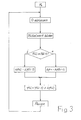
- Fig. 3 ein Flußdiagramm für den Ablauf des Verfahrens.
- Das Verfahren nach der Erfindung ist - wie eingangs bereits erwähnt - sowohl bei der leitungsgebundenen Nachrichtenübertragung über elektrische oder optische Kabel als auch bei der drahtlosen Nachrichtenübertragung einsetzbar. Von besonderer Bedeutung ist das Verfahren bei der Nachrichtenübertragung über elektrische Kabel, in denen symmetrische Doppeladern mit metallischen Leitern zusammengefaßt sind. Im folgenden wird daher - stellvertretend für die anderen Übertragungsmöglichkeiten - das elektrische Kabel als Übertragungsmedium berücksichtigt.
- Die verzerrten und von Störungen überlagerten digitalen Signale gelangen gemäß Fig. 1 von einem Kabel 1 zu einem Empfänger 2, der ein Empfangsfilter 3, eine Abtastvorrichtung 4 und einen Detektor 5 aufweist. Die genauere Ausbildung des Empfängers 2 geht aus Fig. 2 hervor:
- Mit dem Eingang E des Empfängers 2 ist über das Empfangsfilter 3 ein Analog/Digital - Wandler (A/D-Wandler) 6 verbunden, der die Abtastvorrichtung 4 enthält. Auf den A/D-Wandler 6 wirkt ein mit einer Taktgewinnungseinrichtung 7 verbundener Phasenschieber 8 ein. An den A/D-Wandler 6 ist der eine Filter-Einheit 9 und einen Entscheider 10 aufweisende Detektor 5 angeschlossen. Durch den Entscheider 10 werden aus den von der Filter - Einheit 9 gelieferten, aufbereiteten Signalen die ursprünglich gesendeten Quellensignale zurückgewonnen. Einem Summierpunkt 11 werden Eingangssignal ES und Ausgangssignal AS des Entscheiders 10 zugeführt. Das Ausgangssignal AS des Entscheiders 10 kann außerdem der Filter - Einheit 9 zur Auswertung aufgegeben werden. Das im Summierpunkt 11 erzeugte Differenzsignal D wird einer Steuereinheit 12 aufgegeben, die ihrerseits den Phasenschieber 8 an - steuert.
- Die Schaltung nach Fig. 2 arbeitet entsprechend Fig. 3 wie folgt:
- Zu Beginn der Übertragung (Start) wird der Phasenschieber 8 grob eingestellt. Der entsprechende Wert ist in der Steuereinrichtung 12 als Startwert φs gespeichert. Das von dem A/D-Wandler 6 ausgegebene digitale Signal gelangt nach Abtastung und Aufbereitung durch die Filter - Einheit 9 zum Entscheider 10. Dessen Eingangssignal ES und Ausgangssignal AS werden dem Summierpunkt 11 aufgegeben, der aus den beiden zugeführten Signalen die Differenzwerte D bildet. Die Differenzwerte D werden der Steuereinrichtung 12 zugeführt. Sie bildet aus den Differenzwerten D einen Mittelwert. Wenn der Mittelwert stabil ist, wird der Phasenschieber 8 nach Maßgabe des zum Zeitpunkt "i" gegebenen stabilen Mittelwerts M(i) um einen Betrag Δφ in der Phase verstellt.
- Dadurch wird der Abtastzeitpunkt in der Phase verschoben. Die Signale von A/D - Wandler 6 und Filter - Einheit 9 ändern sich. Über den Summierpunkt 11 werden der Steuereinheit 12 weiter Differenzwerte D zugeführt. Sie bildet daraus weiter Mittelwerte. Jeder stabile Mittelwert M(i), der zu einer Verstellung des Phasenschiebers 8 führt, kann in der Steuereinheit 12 gespeichert werden.
- Der Betrag Δφ, um den der Phasenschieber 8 jeweils verstellt wird, ist den Gegebenheiten anzu - passen. Er soll nicht zu klein sein, damit die Adaption des optimalen Abtastzeitpunkts nicht zu lange dauert. Andererseits ist ein zu großer Betrag Δφ nicht sinnvoll, da die Adaption dann mögli - cherweise dauernd hin - und herschwankt und das Optimum u. U. nicht erreicht wird. In bevorzugter Ausführungsform bleibt der Betrag Δφ, um den der Phasenschieber 8 verstellt wird, jeweils gleich. In sinnvoller Betrag für Δφ liegt beispielsweise bei 1 % der gesamten Taktphase. Der Betrag Δφ kann aber auch variabel sein. Das kann zweckmäßig sein, wenn größere Abweichungen auftreten.
- Wenn nach einer Verstellung des Phasen - schiebers 8 ein neuer stabiler Mittelwert M(i) erreicht ist, dann kann eine weitere Verstellung des Phasenschiebers 8 um den gleichen Betrag wie vorher vorgenommen werden. Dazu wird zunächst der neue stabile Mittelwert M(i) mit dem vorange - henden, für eine Verstellung des Phasenschiebers 8 verwendeten stabilen Mittelwert M(i - 1) vergli - chen. Wenn der neue Mittelwert M(i) kleiner ist als der vorangehende, dann war die Verstellung der Phase des Abtastzeitpunkts um den Betrag Δφ in der richtigen Richtung. Die nächste Verstellung um den Betrag Δφ erfolgt dann in der gleichen Rich - tung. Ist der neue Mittelwert M(i) hingegen größer als der vorangehende, dann wird die Phase in entgegengesetzter Richtung um den Betrag Δφ verstellt. Der Zeitpunkt der Verstellung kann au - ßerdem von der Steuereinheit 12 vorgegeben werden. Eine Verstellung erfolgt auf jeden Fall erst dann, wenn das System eingeschwungen und damit der jeweilige Mittelwert M(i) stabil ist. Zwischen zwei Verstellungen des Abtastzeitpunkts liegt dementsprechend eine Pause.
- Als Phasenschieber 8 können beispielsweise digitale Verzögerungsschaltungen oder Laufzeitglieder eingesetzt werden. Die Filter-Einheit 9 besteht vorzugsweise aus Digitalfiltern. Solche Fil - ter sind beispielsweise in der eingangs erwähnten DE - Z "FREQUENZ" beschrieben.
- Bei dem Entscheider 10 kann es sich um ein in der Technik der Nachrichtenübertragung bekanntes Bauteil handeln, wie beispielsweise ein Komparator oder eine Logikschaltung.
- Die Steuereinheit 12 kann ein intelligenter Baustein mit Speichern sein, beispielsweise ein Mikroprozessor oder ein Mikrokontroller. Es können aber auch Gatearrays oder andere Logikschaltun - gen eingesetzt werden.
Claims (5)
Applications Claiming Priority (2)
| Application Number | Priority Date | Filing Date | Title |
|---|---|---|---|
| DE4136474A DE4136474A1 (de) | 1991-11-06 | 1991-11-06 | Verfahren zur digitalen nachrichtenuebertragung |
| DE4136474 | 1991-11-06 |
Publications (3)
| Publication Number | Publication Date |
|---|---|
| EP0540946A2 true EP0540946A2 (de) | 1993-05-12 |
| EP0540946A3 EP0540946A3 (de) | 1994-01-19 |
| EP0540946B1 EP0540946B1 (de) | 1998-01-14 |
Family
ID=6444162
Family Applications (1)
| Application Number | Title | Priority Date | Filing Date |
|---|---|---|---|
| EP92118055A Expired - Lifetime EP0540946B1 (de) | 1991-11-06 | 1992-10-22 | Verfahren zur digitalen Nachrichtenübertragung |
Country Status (8)
| Country | Link |
|---|---|
| EP (1) | EP0540946B1 (de) |
| CN (1) | CN1072301A (de) |
| AT (1) | ATE162351T1 (de) |
| CA (1) | CA2081156A1 (de) |
| DE (2) | DE4136474A1 (de) |
| DK (1) | DK0540946T3 (de) |
| ES (1) | ES2111597T3 (de) |
| IL (1) | IL103624A0 (de) |
Cited By (4)
| Publication number | Priority date | Publication date | Assignee | Title |
|---|---|---|---|---|
| FR2710219A1 (fr) * | 1993-09-13 | 1995-03-24 | Trt Telecom Radio Electr | Dispositif de récupération du rythme d'horloge et modem comportant un tel dispositif. |
| EP1315304A3 (de) * | 2001-11-16 | 2004-03-03 | Philips Intellectual Property & Standards GmbH | Empfangsschaltung zum Empfang von Nachrichtensignalen |
| AT413252B (de) * | 1997-09-29 | 2005-12-15 | Molisch Andreas F Dr | Verfahren zur bestimmung des optimalen abtastzeitpunktes von digitalen signalfolgen mittels trainingsfolgen |
| EP1318638A3 (de) * | 2001-11-16 | 2006-05-17 | Philips Intellectual Property & Standards GmbH | Empfangsschaltung von flankencodierten Signalen unter Verwendung adaptiver Abtastung |
Family Cites Families (1)
| Publication number | Priority date | Publication date | Assignee | Title |
|---|---|---|---|---|
| JPS62298255A (ja) * | 1986-06-18 | 1987-12-25 | Fujitsu Ltd | 識別装置 |
-
1991
- 1991-11-06 DE DE4136474A patent/DE4136474A1/de not_active Withdrawn
-
1992
- 1992-10-22 AT AT92118055T patent/ATE162351T1/de not_active IP Right Cessation
- 1992-10-22 ES ES92118055T patent/ES2111597T3/es not_active Expired - Lifetime
- 1992-10-22 DK DK92118055.0T patent/DK0540946T3/da active
- 1992-10-22 CA CA002081156A patent/CA2081156A1/en not_active Abandoned
- 1992-10-22 EP EP92118055A patent/EP0540946B1/de not_active Expired - Lifetime
- 1992-10-22 DE DE59209132T patent/DE59209132D1/de not_active Expired - Fee Related
- 1992-11-03 IL IL103624A patent/IL103624A0/xx unknown
- 1992-11-06 CN CN92112744.8A patent/CN1072301A/zh active Pending
Cited By (4)
| Publication number | Priority date | Publication date | Assignee | Title |
|---|---|---|---|---|
| FR2710219A1 (fr) * | 1993-09-13 | 1995-03-24 | Trt Telecom Radio Electr | Dispositif de récupération du rythme d'horloge et modem comportant un tel dispositif. |
| AT413252B (de) * | 1997-09-29 | 2005-12-15 | Molisch Andreas F Dr | Verfahren zur bestimmung des optimalen abtastzeitpunktes von digitalen signalfolgen mittels trainingsfolgen |
| EP1315304A3 (de) * | 2001-11-16 | 2004-03-03 | Philips Intellectual Property & Standards GmbH | Empfangsschaltung zum Empfang von Nachrichtensignalen |
| EP1318638A3 (de) * | 2001-11-16 | 2006-05-17 | Philips Intellectual Property & Standards GmbH | Empfangsschaltung von flankencodierten Signalen unter Verwendung adaptiver Abtastung |
Also Published As
| Publication number | Publication date |
|---|---|
| DK0540946T3 (da) | 1998-03-16 |
| ES2111597T3 (es) | 1998-03-16 |
| DE4136474A1 (de) | 1993-05-13 |
| EP0540946B1 (de) | 1998-01-14 |
| CA2081156A1 (en) | 1993-05-07 |
| ATE162351T1 (de) | 1998-01-15 |
| IL103624A0 (en) | 1993-04-04 |
| DE59209132D1 (de) | 1998-02-19 |
| EP0540946A3 (de) | 1994-01-19 |
| CN1072301A (zh) | 1993-05-19 |
Similar Documents
| Publication | Publication Date | Title |
|---|---|---|
| EP0102598B1 (de) | Vorrichtung zur Phasensynchronisierung | |
| DE3604277C2 (de) | Vorrichtung zum Einstellen der Phasenlage von Datensignalen | |
| DE3687114T2 (de) | Datenuebertragungssystem. | |
| EP0412616B1 (de) | Empfänger für zeitvariant verzerrte Datensignale | |
| DE3242577A1 (de) | Endeinrichtung zur digitalen duplexuebertragung ueber eine zweidrahtleitung | |
| DE2056670A1 (de) | Phasen und amplitudenmodulierter Mo | |
| EP0978176A1 (de) | Verfahren zur datenregeneration | |
| EP0356548B1 (de) | Verfahren und Schaltungsanordnung für eine digitale Regelung der Frequenz und/oder der Phase von Abtasttaktimpulsen | |
| EP1470659A1 (de) | Verfahren zur abtastphasenregelung | |
| DE3927681A1 (de) | Verfahren zur zwischenverstaerkung von digitalen signalen sowie zwischenverstaerker fuer digitale signale | |
| DE68908579T2 (de) | Empfänger für ein Datensymbolübertragungssystem mit vorgegebener Baudgeschwindigkeit. | |
| DE3030811A1 (de) | Raumdiversity-empfaenger mit zf-kombinator | |
| WO1998049811A2 (de) | Verfahren und anordnung zur regelung der entscheiderschwelle und des abtastzeitpunktes eines datenregenerators | |
| DE2619964A1 (de) | Anordnung zur impuls-zeitlagekorrektur | |
| EP0540946B1 (de) | Verfahren zur digitalen Nachrichtenübertragung | |
| DE19922804C2 (de) | Taktwiedergewinnungsschaltung | |
| EP0356549B1 (de) | Verfahren und Schaltungsanordnung für eine digitale Regelung der Phase von Abtasttaktimpulsen | |
| EP0133298A1 (de) | Verfahren und Schaltungsanordnung zur Kompensation von Echosignalen | |
| EP0066006B1 (de) | Übersprech- u./o. Echo-Kompensationsschaltung | |
| EP0063638B1 (de) | Digital-Fernmeldesystem | |
| DE19612714A1 (de) | Schaltungsanordnung zur Regeneration eines digitale Datenfolgen enthaltenden Eingangssignals | |
| DE60201030T2 (de) | Empfänger mit einer rückgewinnungsschaltung mittels überabtastung und mehrheitsentscheidung | |
| DE3120434A1 (de) | Adaptive echokompensationseinrichtung zur digitalen duplexuebertragung auf zweidrahtleitungen | |
| DE4220557C2 (de) | Verfahren zur digitalen Nachrichtenübertragung | |
| DE2632165A1 (de) | Schaltungsanordnung zum regeln der folgefrequenz von taktimpulsen |
Legal Events
| Date | Code | Title | Description |
|---|---|---|---|
| PUAI | Public reference made under article 153(3) epc to a published international application that has entered the european phase |
Free format text: ORIGINAL CODE: 0009012 |
|
| AK | Designated contracting states |
Kind code of ref document: A2 Designated state(s): AT BE CH DE DK ES FR GB GR IT LI LU NL PT SE |
|
| PUAL | Search report despatched |
Free format text: ORIGINAL CODE: 0009013 |
|
| AK | Designated contracting states |
Kind code of ref document: A3 Designated state(s): AT BE CH DE DK ES FR GB GR IT LI LU NL PT SE |
|
| 17P | Request for examination filed |
Effective date: 19931208 |
|
| 17Q | First examination report despatched |
Effective date: 19960902 |
|
| GRAG | Despatch of communication of intention to grant |
Free format text: ORIGINAL CODE: EPIDOS AGRA |
|
| GRAG | Despatch of communication of intention to grant |
Free format text: ORIGINAL CODE: EPIDOS AGRA |
|
| GRAH | Despatch of communication of intention to grant a patent |
Free format text: ORIGINAL CODE: EPIDOS IGRA |
|
| GRAH | Despatch of communication of intention to grant a patent |
Free format text: ORIGINAL CODE: EPIDOS IGRA |
|
| RAP1 | Party data changed (applicant data changed or rights of an application transferred) |
Owner name: ALCATEL ALSTHOM COMPAGNIE GENERALE D'ELECTRICITE |
|
| GRAA | (expected) grant |
Free format text: ORIGINAL CODE: 0009210 |
|
| AK | Designated contracting states |
Kind code of ref document: B1 Designated state(s): AT BE CH DE DK ES FR GB GR IT LI LU NL PT SE |
|
| PG25 | Lapsed in a contracting state [announced via postgrant information from national office to epo] |
Ref country code: NL Free format text: LAPSE BECAUSE OF FAILURE TO SUBMIT A TRANSLATION OF THE DESCRIPTION OR TO PAY THE FEE WITHIN THE PRESCRIBED TIME-LIMIT Effective date: 19980114 Ref country code: GR Free format text: LAPSE BECAUSE OF FAILURE TO SUBMIT A TRANSLATION OF THE DESCRIPTION OR TO PAY THE FEE WITHIN THE PRESCRIBED TIME-LIMIT Effective date: 19980114 |
|
| REF | Corresponds to: |
Ref document number: 162351 Country of ref document: AT Date of ref document: 19980115 Kind code of ref document: T |
|
| REG | Reference to a national code |
Ref country code: CH Ref legal event code: EP |
|
| ITF | It: translation for a ep patent filed | ||
| GBT | Gb: translation of ep patent filed (gb section 77(6)(a)/1977) |
Effective date: 19980116 |
|
| REF | Corresponds to: |
Ref document number: 59209132 Country of ref document: DE Date of ref document: 19980219 |
|
| ET | Fr: translation filed | ||
| REG | Reference to a national code |
Ref country code: DK Ref legal event code: T3 Ref country code: ES Ref legal event code: FG2A Ref document number: 2111597 Country of ref document: ES Kind code of ref document: T3 |
|
| PG25 | Lapsed in a contracting state [announced via postgrant information from national office to epo] |
Ref country code: PT Free format text: LAPSE BECAUSE OF FAILURE TO SUBMIT A TRANSLATION OF THE DESCRIPTION OR TO PAY THE FEE WITHIN THE PRESCRIBED TIME-LIMIT Effective date: 19980414 |
|
| REG | Reference to a national code |
Ref country code: CH Ref legal event code: NV Representative=s name: CABINET ROLAND NITHARDT CONSEILS EN PROPRIETE INDU |
|
| NLV1 | Nl: lapsed or annulled due to failure to fulfill the requirements of art. 29p and 29m of the patents act | ||
| PG25 | Lapsed in a contracting state [announced via postgrant information from national office to epo] |
Ref country code: LU Free format text: LAPSE BECAUSE OF NON-PAYMENT OF DUE FEES Effective date: 19981022 |
|
| PLBE | No opposition filed within time limit |
Free format text: ORIGINAL CODE: 0009261 |
|
| STAA | Information on the status of an ep patent application or granted ep patent |
Free format text: STATUS: NO OPPOSITION FILED WITHIN TIME LIMIT |
|
| 26N | No opposition filed | ||
| REG | Reference to a national code |
Ref country code: CH Ref legal event code: PFA Free format text: ALCATEL ALSTHOM COMPAGNIE GENERALE D'ELECTRICITE TRANSFER- ALCATEL SOCIETE ANONYME |
|
| PGFP | Annual fee paid to national office [announced via postgrant information from national office to epo] |
Ref country code: GB Payment date: 19990913 Year of fee payment: 8 |
|
| PGFP | Annual fee paid to national office [announced via postgrant information from national office to epo] |
Ref country code: CH Payment date: 19990915 Year of fee payment: 8 |
|
| PGFP | Annual fee paid to national office [announced via postgrant information from national office to epo] |
Ref country code: SE Payment date: 19990920 Year of fee payment: 8 Ref country code: FR Payment date: 19990920 Year of fee payment: 8 Ref country code: DK Payment date: 19990920 Year of fee payment: 8 |
|
| PGFP | Annual fee paid to national office [announced via postgrant information from national office to epo] |
Ref country code: AT Payment date: 19990923 Year of fee payment: 8 |
|
| PGFP | Annual fee paid to national office [announced via postgrant information from national office to epo] |
Ref country code: DE Payment date: 19990927 Year of fee payment: 8 |
|
| PGFP | Annual fee paid to national office [announced via postgrant information from national office to epo] |
Ref country code: BE Payment date: 19990929 Year of fee payment: 8 |
|
| PGFP | Annual fee paid to national office [announced via postgrant information from national office to epo] |
Ref country code: ES Payment date: 19991020 Year of fee payment: 8 |
|
| REG | Reference to a national code |
Ref country code: FR Ref legal event code: CD |
|
| PG25 | Lapsed in a contracting state [announced via postgrant information from national office to epo] |
Ref country code: GB Free format text: LAPSE BECAUSE OF NON-PAYMENT OF DUE FEES Effective date: 20001022 Ref country code: DK Free format text: LAPSE BECAUSE OF NON-PAYMENT OF DUE FEES Effective date: 20001022 Ref country code: AT Free format text: LAPSE BECAUSE OF NON-PAYMENT OF DUE FEES Effective date: 20001022 |
|
| PG25 | Lapsed in a contracting state [announced via postgrant information from national office to epo] |
Ref country code: ES Free format text: LAPSE BECAUSE OF NON-PAYMENT OF DUE FEES Effective date: 20001023 |
|
| PG25 | Lapsed in a contracting state [announced via postgrant information from national office to epo] |
Ref country code: SE Free format text: THE PATENT HAS BEEN ANNULLED BY A DECISION OF A NATIONAL AUTHORITY Effective date: 20001030 |
|
| PG25 | Lapsed in a contracting state [announced via postgrant information from national office to epo] |
Ref country code: LI Free format text: LAPSE BECAUSE OF NON-PAYMENT OF DUE FEES Effective date: 20001031 Ref country code: CH Free format text: LAPSE BECAUSE OF NON-PAYMENT OF DUE FEES Effective date: 20001031 Ref country code: BE Free format text: LAPSE BECAUSE OF NON-PAYMENT OF DUE FEES Effective date: 20001031 |
|
| BERE | Be: lapsed |
Owner name: ALCATEL Effective date: 20001031 |
|
| REG | Reference to a national code |
Ref country code: DK Ref legal event code: EBP |
|
| GBPC | Gb: european patent ceased through non-payment of renewal fee |
Effective date: 20001022 |
|
| REG | Reference to a national code |
Ref country code: CH Ref legal event code: PL |
|
| EUG | Se: european patent has lapsed |
Ref document number: 92118055.0 |
|
| PG25 | Lapsed in a contracting state [announced via postgrant information from national office to epo] |
Ref country code: FR Free format text: LAPSE BECAUSE OF NON-PAYMENT OF DUE FEES Effective date: 20010629 |
|
| PG25 | Lapsed in a contracting state [announced via postgrant information from national office to epo] |
Ref country code: DE Free format text: LAPSE BECAUSE OF NON-PAYMENT OF DUE FEES Effective date: 20010703 |
|
| REG | Reference to a national code |
Ref country code: FR Ref legal event code: ST |
|
| REG | Reference to a national code |
Ref country code: ES Ref legal event code: FD2A Effective date: 20011113 |
|
| PG25 | Lapsed in a contracting state [announced via postgrant information from national office to epo] |
Ref country code: IT Free format text: LAPSE BECAUSE OF NON-PAYMENT OF DUE FEES;WARNING: LAPSES OF ITALIAN PATENTS WITH EFFECTIVE DATE BEFORE 2007 MAY HAVE OCCURRED AT ANY TIME BEFORE 2007. THE CORRECT EFFECTIVE DATE MAY BE DIFFERENT FROM THE ONE RECORDED. Effective date: 20051022 |