EP0542263A1 - Halbleiterbauelement und niedrigen Widerstandswerken an Verbindungsstellen der leitenden Schichten - Google Patents
Halbleiterbauelement und niedrigen Widerstandswerken an Verbindungsstellen der leitenden Schichten Download PDFInfo
- Publication number
- EP0542263A1 EP0542263A1 EP92119365A EP92119365A EP0542263A1 EP 0542263 A1 EP0542263 A1 EP 0542263A1 EP 92119365 A EP92119365 A EP 92119365A EP 92119365 A EP92119365 A EP 92119365A EP 0542263 A1 EP0542263 A1 EP 0542263A1
- Authority
- EP
- European Patent Office
- Prior art keywords
- primary
- conductor
- conductor film
- insulator
- layer
- Prior art date
- Legal status (The legal status is an assumption and is not a legal conclusion. Google has not performed a legal analysis and makes no representation as to the accuracy of the status listed.)
- Ceased
Links
Images


Classifications
-
- H—ELECTRICITY
- H10—SEMICONDUCTOR DEVICES; ELECTRIC SOLID-STATE DEVICES NOT OTHERWISE PROVIDED FOR
- H10W—GENERIC PACKAGES, INTERCONNECTIONS, CONNECTORS OR OTHER CONSTRUCTIONAL DETAILS OF DEVICES COVERED BY CLASS H10
- H10W20/00—Interconnections in chips, wafers or substrates
- H10W20/40—Interconnections external to wafers or substrates, e.g. back-end-of-line [BEOL] metallisations or vias connecting to gate electrodes
- H10W20/41—Interconnections external to wafers or substrates, e.g. back-end-of-line [BEOL] metallisations or vias connecting to gate electrodes characterised by their conductive parts
- H10W20/42—Vias, e.g. via plugs
-
- H—ELECTRICITY
- H10—SEMICONDUCTOR DEVICES; ELECTRIC SOLID-STATE DEVICES NOT OTHERWISE PROVIDED FOR
- H10W—GENERIC PACKAGES, INTERCONNECTIONS, CONNECTORS OR OTHER CONSTRUCTIONAL DETAILS OF DEVICES COVERED BY CLASS H10
- H10W20/00—Interconnections in chips, wafers or substrates
- H10W20/40—Interconnections external to wafers or substrates, e.g. back-end-of-line [BEOL] metallisations or vias connecting to gate electrodes
- H10W20/41—Interconnections external to wafers or substrates, e.g. back-end-of-line [BEOL] metallisations or vias connecting to gate electrodes characterised by their conductive parts
- H10W20/44—Conductive materials thereof
- H10W20/4403—Conductive materials thereof based on metals, e.g. alloys, metal silicides
- H10W20/4432—Conductive materials thereof based on metals, e.g. alloys, metal silicides the principal metal being a noble metal, e.g. gold
- H10W20/4435—Noble-metal alloys
Definitions
- This invention relates to a semiconductor device having a plurality of conductor layers.
- a conventional semiconductor device comprises a semiconductor substrate, a first insulator layer, a first conductor layer, a second insulator layer, and a second conductor layer.
- the semiconductor substrate has a principal surface.
- the first insulator layer overlies the principal surface and has a first upper insulator surface.
- the first conductor layer overlies the first upper insulator surface and has a first upper conductor surface leaving a surrounding area of the first upper insulator surface.
- the second insulator layer overlies the first upper conductor surface and the surrounding area and has a second upper insulator surface.
- the second insulator layer has a recessed surface which defines a contact perforation exposing a predetermined area of said first upper conductor surface.
- the second conductor layer comprises a primary conductor film and a secondary conductor film. The primary conductor film overlies the second insulator surface, the recessed surface, and predetermined area and has a primary upper surface.
- the secondary conductor film overlies the primary upper surface.
- the secondary conductor film is connected to the first conductor layer through the primary conductor film.
- the primary conductor film has a first resistance value which is high. Consequently, a resistance value at a connection point of the first and the second conductor layers is high.
- This conventional semiconductor device comprises a semiconductor substrate, a first insulator layer, a first conductor layer, a second insulator layer, and a second conductor layer.
- the semiconductor substrate has a principal surface.
- the first insulator layer overlies the principal surface and has a first upper insulator surface.
- the first conductor layer overlies the first upper insulator surface and has a first upper conductor surface leaving a surrounding area of the first upper insulator surface.
- the second insulator layer overlies the first upper conductor surface and the surrounding area and has a second upper insulator surface.
- the second insulator layer has a first recessed surface which defines a first contact perforation exposing a predetermined area of the first upper conductor surface.
- the second conductor layer comprises a primary conductor film and a secondary conductor film.
- the primary conductor film overlies a second upper insulator surface and has a primary upper surface.
- the primary conductor film has a second recessed surface which defines a second contact perforation exposing, in combination with the first contact perforation, the predetermined area of the first upper conductor surface.
- the secondary conductor film overlies the primary upper surface, the first and the second recessed surfaces, and the predetermined area. Namely, the secondary conductor film is directly connected to the first conductor layer.
- the secondary film is made of gold. In this event, the secondary film can not be formed on the second recessed surface by electroplating without a conductor film on the second recessed surface.
- a semiconductor device which comprises (A) a semiconductor substrate having a principal surface; (B) a first insulator layer overlying the principal surface and having a first upper insulator surface; (C) a first conductor layer overlying the first upper insulator surface and having a first upper conductor surface leaving a surrounding area of the first upper insulator surface; (D) a second insulator layer overlying the first upper conductor surface and the surrounding area of the first upper insulator surface and having a second upper insulator surface, the second insulator layer having a recessed surface which defines a contact perforation exposing a predetermined area of the first upper conductor surface; and (E) a second conductor layer overlying the second upper insulator surface, the recessed surface, and the predetermined area, the second conductor layer comprising a primary conductor film having a primary upper surface, a secondary conductor film having a secondary upper surface, and a ternary conductor film, the primary conductor
- a method which is for manufacturing a semiconductor device and which comprises the steps of: (A) preparing a semiconductor substrate having a principal surface; (B) forming a first insulator layer on the principal surface to have a first upper insulator surface; (C) forming a first conductor layer on the first upper insulator surface leaving a surrounding area of the first upper insulator surface, the first conductor layer having a first upper conductor surface; (D) forming a second insulator layer on the first upper conductor surface and the surrounding area of the first upper insulator surface to have a second upper insulator surface; (E) forming in the second insulator layer a first recessed surface which defines a first contact perforation exposing a predetermined area of the first upper conductor surface; and (F) forming a second conductor layer on the second upper insulator surface, the first recessed surface, and the predetermined area; (G) the second conductor layer forming step comprising: (H) forming a first insulator layer on the principal surface
- a method which is for manufacturing a semiconductor device and which comprises the steps of: (A) preparing a semiconductor substrate having a principal surface; (B) forming a first insulator layer on the principal surface to have a first upper insulator surface; (C) forming a first conductor layer on the first upper insulator surface leaving a surrounding area of the first upper insulator surface, the first conductor layer having a first upper conductor surface; (D) forming a second insulator layer on the first upper conductor surface and the surrounding area of the first upper insulator surface to have a second upper insulator surface; (E) forming a primary conductor film on the second upper insulator surface to have a primary resistance value and a primary upper surface; (F) forming in the primary conductor film a first recessed surface which defines a first contact perforation; (G) forming in the second insulator layer a second recessed surface which defines a second contact perforation exposing, in combination
- the conventional semiconductor device comprises a semiconductor substrate 21, a first insulator layer 23, first primary and secondary conductor layers 25 and 27, a second insulator layer 29, and a second conductor layer 31.
- the semiconductor substrate 21 has a principal surface 21a.
- the first insulator layer 23 overlies the principal surface 21a and has a first upper insulator surface 23a.
- the first insulator layer 23 has a first recessed surface 23b which defines a first contact perforation exposing a first predetermined area of the principal surface 21a.
- the first primary conductor layer 25 overlies the first upper insulator surface 23a and has a first primary upper conductor surface 25a leaving a primary surrounding area of the first upper insulator surface 23a.
- the first secondary conductor layer 27 overlies the first predetermined area of the principal surface 21a and the first upper insulator surface 23a.
- the first secondary conductor layer 27 has a first secondary upper conductor surface 27a leaving a secondary surrounding area of the first upper insulator surface 23a.
- the second insulator layer 29 overlies the first primary and the first secondary upper conductor surfaces 25a and 27a and the primary and the secondary surrounding areas.
- the second insulator layer 29 has a second upper insulator surface 29a.
- the second insulator layer 29 has a second recessed surface 29b which defines a second contact perforation exposing a second predetermined area of the first primary upper conductor surface 25a.
- the second conductor layer 31 comprises a primary conductor film 35 and a secondary conductor film 37.
- the primary conductor film 35 overlies the second upper insulator surface 29a, the second recessed surface 29b, and the second predetermined area of the first primary upper conductor surface 25a.
- the primary conductor film 35 has a primary upper surface 35a.
- the secondary conductor film 37 overlies the primary upper surface 35a.
- the first primary and the first secondary conductor layers 25 and 27 are made of aluminum, aluminum alloy, or aluminum copper alloy.
- the primary conductor film 35 is made of titanium or tungsten.
- the secondary conductor film 37 is made of aluminum or aluminum alloy.
- another conventional semiconductor device further comprises primary through quaternary films 41, 42, 43, and 44.
- the primary film 41 overlies the first upper insulator surface 23a and has a primary upper film surface 41a.
- the secondary film 42 overlies the primary upper film surface 41a and has a secondary upper film surface 42a.
- the first primary conductor layer 25 overlies the secondary upper film surface 42a.
- the ternary film 43 overlies the first upper insulator surface 23a and the first predetermined area of the principal surface 21a and has a ternary upper film surface 43a.
- the quaternary film 44 overlies the ternary upper film surface 43a and has a quaternary upper film surface 44a.
- the first secondary conductor layer 27 overlies the quaternary upper film surface 44a.
- the first primary and the first secondary conductor layers 25 and 27 are made of gold.
- the primary conductor film 35 is made of titanium tungsten alloy.
- the secondary conductor film 37 is made of gold.
- the primary and the ternary conductor films 41 and 43 are made of titanium tungsten alloy.
- the secondary and the quaternary conductor films 42 and 44 are made of platinum.
- the secondary conductor film 37 is connected to the first primary conductor layer 25 through the primary conductor film 35.
- the primary conductor film 35 has a primary resistance value which is high. Consequently, a resistance value at a connection point of the first primary conductor layer 25 and the second conductor layer 31 is high.
- a first curved line A exemplifies a relation of resistance values in response to diameters at a connection point of the first primary conductor layer 25 and the second conductor layer 31 in the conventional semiconductor device illustrated in Fig. 2.
- a second curved line B will later be described.
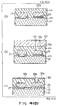
- the semiconductor substrate 21 was prepared in the known manner to have the principal surface 21a.
- the semiconductor substrate 21 was made of inorganic semiconductor compound to have diffusion layers (not shown).
- the first insulator layer 23 was formed on the principal surface 21a to have the first upper insulator surface 23a.
- the first insulator layer 23 was formed by photo lithography and dry etching to have the first recessed surface 23b which defines the first contact perforation exposing a first predetermined area of the principal surface 21a.
- a first film 51 was formed by sputter of titanimum tungsten alloy onto the first upper insulator surface 21a and the first predetermined area to have a first upper surface.
- a second film 52 was formed by sputter of platinum onto the first upper surface of the first film 51 to have a second upper surface.
- first-set photo resists 55 were formed by photo lithography on the second upper surface of the second film 52 with a gap left between adjacent two photo resists 55.
- Each of the first primary and the first secondary conductor layers 25 and 27 was formed by electroplating gold or gold alloy on the second upper surface of the second film 52 between the photo resists 55.
- the photo resists 55 were taken away from the second upper surface of the second film 52.
- a first predetermined part of the first film 51 and a second predetermined part of the second film 52 were taken away either by wet etching or by sputter etching with the first primary and the first secondary conductor layers 25 and 27 used as masks.
- the primary through the quaternary films 41 to 44 and the first primary and the first secondary conductor layers 25 and 27 were formed.
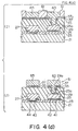
- the second insulator layer 29 was formed on the first primary and the first secondary upper conductor surfaces 25a and 27a and the first upper insulator surface 23a to have the second upper insulator surface 29a.
- the second insulator layer 29 was formed by plasma CVD (chemical vapor deposition) process of either an oxide film or a nitride film.
- the second insulator layer 29 may be an inorganic film, such as Si x O y N z .
- a second photo resist 57 was formed by photo lithography on the second upper insulator surface 29a to have a first recessed resist surface 57a which defines a perforation exposing a third predetermined area of the second upper insulator surface 29a.
- the second insulator layer 29 was formed by wet or dry etching with the second photo resist 57 used as a mask to have the second recessed surface 29b which defines the second contact perforation exposing the second predetermined area of the first primary upper conductor surface 25a.
- the primary conductor film 35 was formed on the second upper insulator surface 29a, the second recessed surface 29b, and the second predetermined area of the first primary upper conductor surface 25a to have the primary upper surface 35a.
- the primary conductor film 35 was formed by sputter of at least one member selected from titanium, tungsten, molybdenum, and titanium nitride.
- the primary conductor film 35 may be made by sputter of a silicide of at least one member selected from titanium, tungsten, molybdenum, and titanium nitride.
- a third photo resist 59 was formed by photo lithography on the primary upper surface 35a to have a second recessed resist surface 59a which defines the perforation exposing a fourth predetermined area of the primary upper surface 35a.
- the primary conductor film 35 was formed by wet or dry etching to have the third recessed surface 35b which defines the third contact perforation exposing, in combination with the second recessed surface 29a, the second predetermined area of the first primary upper conductor surface 25a.
- the secondary conductor film 37 was formed by sputter on the primary upper surface 35a, the second and the third recessed surfaces 29b and 35b, and the second predetermined area of the first primary upper conductor surface 35a.
- the secondary conductor film 37 was made of a member selected from platinum, palladium, platinum alloy, and palladium alloy.
- Third-set resists 61 were formed by photo lithography on the secondary upper surface 37a with a gap left between adjacent two photo resists 61.
- each of a first ternary conductor film 63 and a second ternary conductor film 65 was formed by electroplating gold on the secondary upper surface 37a between the third-set resists 61.
- the third-set resists 61 were taken away from the secondary upper surface 37a.
- a primary predetermined part of the primary conductor film 35 and a secondary predetermined part of the secondary conductor film 37 were taken away by wet etching or sputter etching with the first ternary conductor film 63 and the second ternary conductor film 65 used as masks.
- the second conductor layers 31 comprises the primary conductor film 35, the secondary conductor film 37, and the first ternary conductor film 63. Although not shown, one or more second conductor layer, such as 31, may additionally be formed on the first ternary conductor film 63 in the manner described in connection with Figs. 4(D) to (J).
- the illustrated semiconductor device is manufactured like the device of Fig. 4 with a process of Fig. 5 carried out instead of processes of Figs. 4(E) and (F).
- the primary conductor film 35 was formed on the second insulator surface 29a by sputter of at least one member selected from titanium, tungsten, molybdenum, and titanium nitride.
- the primary conductor film 35 may be made by sputter of a silicide of at least one member selected from titanium, tungsten, molybdenum, and titanium nitride.
- the semiconductor substrate 21 has a thickness of 200 to 800 microns.
- the first insulator layer 23 has a thickness of 0.1 to 1.5 microns.
- the first primary and the first secondary layers 25 and 27 has a thickness of 0.4 to 1.2 microns.
- the second insulator layer 29 has a thickness of 1.0 to 1.5 microns.
- the primary conductor film 35 has a thickness of 0.1 to 0.3 micron.
- the secondary conductor film 31 has a thickness of 0.01 to 0.03 micron.
- Each of the first and the second ternary conductor films 63 and 65 has a thickness of 0.4 to 1.2 microns.
- Each of the primary and the ternary films 41 and 43 has a thickness of 0.03 to 0.2 micron.
- Each of the secondary and the quaternary films 42 and 44 has a thickness of 0.03 to 0.1 micron.
- the primary conductor film 35 has a primary resistance value.
- the secondary conductor film 37 has a secondary resistance value which is lower than the primary resistance value.
- the second curved line B exemplifies a relation of resistance values in response to diameters at a connection point of the first primary conductor layer 25 and the second conductor layer 31 in the semiconductor device eventually attained at the step illustrated in Fig. 4(J).
- the connection point of the first primary conductor layer 25 and the second conductor layer 31 is the secondary conductor film 35 and the first ternary conductor film 37 in the second contact perforation which is defined by the second recessed surface 29a.
Landscapes
- Internal Circuitry In Semiconductor Integrated Circuit Devices (AREA)
- Electrodes Of Semiconductors (AREA)
- Semiconductor Integrated Circuits (AREA)
Applications Claiming Priority (2)
| Application Number | Priority Date | Filing Date | Title |
|---|---|---|---|
| JP3295319A JPH05206134A (ja) | 1991-11-12 | 1991-11-12 | 半導体装置とその製造方法 |
| JP295319/91 | 1991-11-12 |
Publications (1)
| Publication Number | Publication Date |
|---|---|
| EP0542263A1 true EP0542263A1 (de) | 1993-05-19 |
Family
ID=17819077
Family Applications (1)
| Application Number | Title | Priority Date | Filing Date |
|---|---|---|---|
| EP92119365A Ceased EP0542263A1 (de) | 1991-11-12 | 1992-11-12 | Halbleiterbauelement und niedrigen Widerstandswerken an Verbindungsstellen der leitenden Schichten |
Country Status (3)
| Country | Link |
|---|---|
| US (1) | US5500560A (de) |
| EP (1) | EP0542263A1 (de) |
| JP (1) | JPH05206134A (de) |
Cited By (1)
| Publication number | Priority date | Publication date | Assignee | Title |
|---|---|---|---|---|
| CN111433909A (zh) * | 2017-12-14 | 2020-07-17 | 三菱电机株式会社 | 半导体装置 |
Families Citing this family (4)
| Publication number | Priority date | Publication date | Assignee | Title |
|---|---|---|---|---|
| JPH07263555A (ja) * | 1994-03-24 | 1995-10-13 | Nec Corp | 半導体装置の製造方法 |
| JP3168400B2 (ja) * | 1996-01-19 | 2001-05-21 | 日本プレシジョン・サーキッツ株式会社 | 半導体装置および半導体装置の製造方法 |
| JP3719618B2 (ja) | 1996-06-17 | 2005-11-24 | 松下電器産業株式会社 | 半導体装置及びその製造方法 |
| CA2374887A1 (en) * | 1999-05-26 | 2000-11-30 | Henkel Corporation | Autodeposition coatings and process therefor |
Citations (3)
| Publication number | Priority date | Publication date | Assignee | Title |
|---|---|---|---|---|
| EP0310108A2 (de) * | 1987-10-02 | 1989-04-05 | Kabushiki Kaisha Toshiba | Verbindungsstruktur eines Halbleiterbauelementes und Verfahren zu ihrer Herstellung |
| US4874719A (en) * | 1986-05-06 | 1989-10-17 | Kabushiki Kaisha Toshiba | Method for manufacturing an electrical connection between conductor levels |
| EP0343698A1 (de) * | 1988-04-22 | 1989-11-29 | Koninklijke Philips Electronics N.V. | Herstellungsverfahren für Verbindungsstrukturen auf einem Halbleiterbauelement, besonders auf einem hochintegrierten Schaltkreis |
Family Cites Families (17)
| Publication number | Priority date | Publication date | Assignee | Title |
|---|---|---|---|---|
| DE2012110A1 (de) * | 1970-03-13 | 1971-09-23 | Siemens Ag | Verfahren zum Herstellen einer Mehrlagenmetallisierung an elektrischen Bauelementen |
| US3926747A (en) * | 1974-02-19 | 1975-12-16 | Bell Telephone Labor Inc | Selective electrodeposition of gold on electronic devices |
| US4121241A (en) * | 1977-01-03 | 1978-10-17 | Raytheon Company | Multilayer interconnected structure for semiconductor integrated circuit |
| JPS564234A (en) * | 1979-06-26 | 1981-01-17 | Toshiba Corp | Manufacture of semiconductor device |
| JPS58137231A (ja) * | 1982-02-09 | 1983-08-15 | Nec Corp | 集積回路装置 |
| US4755480A (en) * | 1986-02-03 | 1988-07-05 | Intel Corporation | Method of making a silicon nitride resistor using plasma enhanced chemical vapor deposition |
| JPH079935B2 (ja) * | 1986-08-13 | 1995-02-01 | 日本電気株式会社 | 半導体装置 |
| US4872050A (en) * | 1988-03-15 | 1989-10-03 | Mitsubishi Denki Kabushiki Kaisha | Interconnection structure in semiconductor device and manufacturing method of the same |
| JPH01255249A (ja) * | 1988-04-04 | 1989-10-12 | Nec Corp | 半導体集積回路装置 |
| JPH01270347A (ja) * | 1988-04-22 | 1989-10-27 | Sony Corp | 半導体装置 |
| JPH02200764A (ja) * | 1989-01-31 | 1990-08-09 | Dainippon Printing Co Ltd | 金属被覆処理におけるマスキング方法 |
| JP2537413B2 (ja) * | 1989-03-14 | 1996-09-25 | 三菱電機株式会社 | 半導体装置およびその製造方法 |
| JPH036045A (ja) * | 1989-06-02 | 1991-01-11 | Fujitsu Ltd | 半導体装置の製造方法 |
| JPH039524A (ja) * | 1989-06-07 | 1991-01-17 | Fujitsu Ltd | 半導体装置 |
| JPH03250627A (ja) * | 1990-01-31 | 1991-11-08 | Fujitsu Ltd | 半導体装置及びその製造方法 |
| JP3111466B2 (ja) * | 1990-09-07 | 2000-11-20 | セイコーエプソン株式会社 | メッキ配線層を備えた半導体装置の製造方法 |
| JPH05109901A (ja) * | 1991-10-18 | 1993-04-30 | Seiko Epson Corp | 多層配線構造を備えた半導体装置及びその製造方法 |
-
1991
- 1991-11-12 JP JP3295319A patent/JPH05206134A/ja active Pending
-
1992
- 1992-11-12 EP EP92119365A patent/EP0542263A1/de not_active Ceased
- 1992-11-12 US US07/974,719 patent/US5500560A/en not_active Expired - Fee Related
Patent Citations (3)
| Publication number | Priority date | Publication date | Assignee | Title |
|---|---|---|---|---|
| US4874719A (en) * | 1986-05-06 | 1989-10-17 | Kabushiki Kaisha Toshiba | Method for manufacturing an electrical connection between conductor levels |
| EP0310108A2 (de) * | 1987-10-02 | 1989-04-05 | Kabushiki Kaisha Toshiba | Verbindungsstruktur eines Halbleiterbauelementes und Verfahren zu ihrer Herstellung |
| EP0343698A1 (de) * | 1988-04-22 | 1989-11-29 | Koninklijke Philips Electronics N.V. | Herstellungsverfahren für Verbindungsstrukturen auf einem Halbleiterbauelement, besonders auf einem hochintegrierten Schaltkreis |
Non-Patent Citations (1)
| Title |
|---|
| DATABASE WPIL Section Ch, Week 9010, Derwent Publications Ltd., London, GB; Class L03, AN 90-071014 & JP-A-2 023 639 (FUJITSU LTD) 25 January 1990 * |
Cited By (2)
| Publication number | Priority date | Publication date | Assignee | Title |
|---|---|---|---|---|
| CN111433909A (zh) * | 2017-12-14 | 2020-07-17 | 三菱电机株式会社 | 半导体装置 |
| CN111433909B (zh) * | 2017-12-14 | 2023-08-11 | 三菱电机株式会社 | 半导体装置 |
Also Published As
| Publication number | Publication date |
|---|---|
| JPH05206134A (ja) | 1993-08-13 |
| US5500560A (en) | 1996-03-19 |
Similar Documents
| Publication | Publication Date | Title |
|---|---|---|
| EP0143652B1 (de) | Verfahren zum Herstellen von Mehrschicht-Leiterbahnen | |
| US5275973A (en) | Method for forming metallization in an integrated circuit | |
| JP2785768B2 (ja) | 半導体装置の製造方法 | |
| TW202001998A (zh) | 具有層心軸之自對準多重圖案化製程 | |
| JPH0774250A (ja) | コンタクトホール形成方法 | |
| US5726098A (en) | Method of manufacturing semiconductor device having multilevel interconnection | |
| US5500560A (en) | Semiconductor device having low resistance values at connection points of conductor layers | |
| US6831007B2 (en) | Method for forming metal line of Al/Cu structure | |
| US5686358A (en) | Method for forming a plug in a semiconductor device | |
| EP0203800A2 (de) | Verfahren zur Herstellung einer halbleiteranordnung | |
| US5184205A (en) | Semiconductor device having multi-layered wiring, and method of manufacturing the same | |
| US5466640A (en) | Method for forming a metal wire of a semiconductor device | |
| GB2245759A (en) | Method of forming a tungsten interconnection pattern on a semiconductor device | |
| US6586325B2 (en) | Process for making an electronic device having a multilevel structure | |
| JPH09199588A (ja) | 半導体装置の製造方法 | |
| KR0156122B1 (ko) | 반도체장치의 제조방법 | |
| JPS5966125A (ja) | 半導体装置の製造方法 | |
| JP3329148B2 (ja) | 配線形成方法 | |
| JP2000031271A (ja) | 多層配線の半導体装置の製造方法 | |
| JPS5994457A (ja) | 半導体装置 | |
| KR0167251B1 (ko) | 반도체 소자의 배선구조 및 그 제조방법 | |
| KR100197129B1 (ko) | 반도체 소자의 금속배선 형성방법 | |
| JP2823727B2 (ja) | コンタクト形成方法 | |
| JPH08274098A (ja) | 半導体装置及び半導体装置の製造方法 | |
| KR970013212A (ko) | 반도체 소자의 배선구조 및 그 제조방법 |
Legal Events
| Date | Code | Title | Description |
|---|---|---|---|
| PUAI | Public reference made under article 153(3) epc to a published international application that has entered the european phase |
Free format text: ORIGINAL CODE: 0009012 |
|
| 17P | Request for examination filed |
Effective date: 19930215 |
|
| AK | Designated contracting states |
Kind code of ref document: A1 Designated state(s): DE FR GB |
|
| 17Q | First examination report despatched |
Effective date: 19941219 |
|
| STAA | Information on the status of an ep patent application or granted ep patent |
Free format text: STATUS: THE APPLICATION HAS BEEN REFUSED |
|
| 18R | Application refused |
Effective date: 19970531 |