EP0542633A1 - Modulateur notamment pour systèmes de téléphones numétrique cellulaires - Google Patents
Modulateur notamment pour systèmes de téléphones numétrique cellulaires Download PDFInfo
- Publication number
- EP0542633A1 EP0542633A1 EP92403067A EP92403067A EP0542633A1 EP 0542633 A1 EP0542633 A1 EP 0542633A1 EP 92403067 A EP92403067 A EP 92403067A EP 92403067 A EP92403067 A EP 92403067A EP 0542633 A1 EP0542633 A1 EP 0542633A1
- Authority
- EP
- European Patent Office
- Prior art keywords
- modulator
- processor
- peripheral processor
- cos
- modulator according
- Prior art date
- Legal status (The legal status is an assumption and is not a legal conclusion. Google has not performed a legal analysis and makes no representation as to the accuracy of the status listed.)
- Granted
Links
- 230000001413 cellular effect Effects 0.000 title claims abstract description 4
- 230000002093 peripheral effect Effects 0.000 claims abstract description 13
- 230000015654 memory Effects 0.000 claims description 26
- 230000006870 function Effects 0.000 claims description 5
- 238000010586 diagram Methods 0.000 description 9
- 230000000875 corresponding effect Effects 0.000 description 6
- 238000005070 sampling Methods 0.000 description 6
- 238000000034 method Methods 0.000 description 4
- 238000010276 construction Methods 0.000 description 3
- 230000002596 correlated effect Effects 0.000 description 3
- 230000004044 response Effects 0.000 description 3
- 239000004020 conductor Substances 0.000 description 2
- 230000005236 sound signal Effects 0.000 description 2
- 238000012546 transfer Methods 0.000 description 2
- 101000996048 Arabidopsis thaliana Non-specific lipid-transfer protein 13 Proteins 0.000 description 1
- XUIMIQQOPSSXEZ-UHFFFAOYSA-N Silicon Chemical compound [Si] XUIMIQQOPSSXEZ-UHFFFAOYSA-N 0.000 description 1
- 230000005540 biological transmission Effects 0.000 description 1
- 238000004891 communication Methods 0.000 description 1
- 238000005516 engineering process Methods 0.000 description 1
- 238000001914 filtration Methods 0.000 description 1
- 238000012545 processing Methods 0.000 description 1
- 229910052710 silicon Inorganic materials 0.000 description 1
- 239000010703 silicon Substances 0.000 description 1
- 238000012360 testing method Methods 0.000 description 1
- 230000007704 transition Effects 0.000 description 1
Images



Classifications
-
- H—ELECTRICITY
- H04—ELECTRIC COMMUNICATION TECHNIQUE
- H04L—TRANSMISSION OF DIGITAL INFORMATION, e.g. TELEGRAPHIC COMMUNICATION
- H04L27/00—Modulated-carrier systems
- H04L27/18—Phase-modulated carrier systems, i.e. using phase-shift keying
- H04L27/20—Modulator circuits; Transmitter circuits
- H04L27/2003—Modulator circuits; Transmitter circuits for continuous phase modulation
- H04L27/2007—Modulator circuits; Transmitter circuits for continuous phase modulation in which the phase change within each symbol period is constrained
- H04L27/2017—Modulator circuits; Transmitter circuits for continuous phase modulation in which the phase change within each symbol period is constrained in which the phase changes are non-linear, e.g. generalized and Gaussian minimum shift keying, tamed frequency modulation
Definitions
- the present invention relates to the digital cellular telephone systems using the time division multiple access (TDMA) method, for example the GSM method.
- TDMA time division multiple access
- TDMA time division multiple access method
- the modulator which is an element whose task is indivisible is implemented with a dedicated operator activated for a constant period of time.
- the maximum value of this ratio for the modulator is 12.5%, but overall it is less than 0.2%.
- circuitry resources necessary for this operator cannot be re-used to carry out other tasks during the periods of inactivity.
- This digital modulator operator is usually implemented within linear parts, close to converters and requires a mixed digital/linear technology which is a penal ty on the digital part.
- the invention proposes to remedy these drawbacks by creating a modulator/demodulator whose construction does not compromise the operation of digital circuits with which it might be associated.
- the subject is therefore a digital modulator, characterised in that it comprises a programmable peripheral processor carrying out, with the same circuits, the modulation function and the channel coder/ decoder tasks.
- the terminal of the time division multiple access type represented in Fig. 1 comprises a vocoder 1 receiving an audio signal on one input 2 and delivering an audio signal on an output signal on an output 3.
- the vocoder 1 is, for example, of the RPE - LTP 13 KBT/S of the GSM type.
- a coder-decoder 4 one output of which is linked to a modulator 5 delivering, at its outputs, I and Q signals to a linear circuit and one input of which is linked to a demodulator 6 whose inputs receive the I and Q signals originating from the linear circuit.
- the coder-decoder 4 is, for example, a bit manipulation coder with convolution coding and Viterbi decoding.
- the modulator 5 is based on a ROM while the demodulator 6 comprises a complex-type short-word processor.
- the circuits 1, 4 and 6 are connected to a control circuit 7 which also comprises a communication output with an external application.
- the modulator 5 represented in more detail in Fig. 2 mainly comprises a three-stage shift register 8 whose input receives binary data from the coder-decoder 4 (Fig. 1) and which comprises an output linked to a phase ⁇ state counter 9.
- a modulo 4 counter 10 receives input signals from the sampling clock.
- the shift register 8 delivers 3-bit signals on a second output.
- the ⁇ state counter 9 delivers 2-bit signals at its output.
- the modulo 4 counter 10 delivers 2-bit signals at its output.
- the 3- and 2- bit outputs, of the three abovementioned circuits are connected to corresponding inputs of a 7-bit decoder 11.
- the output of the decoder 11 is linked to a coded wave form memory 12 which is subdivided into a I-coded 128 word ROM memory 13 and a Q-coded 128 word ROM memory 14.
- the outputs of the ROM memories 13 and 14 are connected to a bus control circuit 15 whose outputs are, in their turn, linked to digital-analog converters 16 and 17 for the Q and I signals controlled by the sampling clock signals applied to the modulo 4 counter 10.
- the analog output of the Q signals from the converter 16 is linked to the input of a linear phase filter 18 while the output of the converter 17 is connected to the input of another linear phase filter 19.
- the outputs of the filters 18 and 19 are connected respectively to multipliers 20 and 21 which moreover receive signals sin[ ⁇ ot] and cos[ ⁇ ot] and which deliver Q and I signals at their outputs.
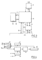
- peripheral processor of the modulator according to the invention is represented diagrammatically in Fig. 3.
- It comprises a peripheral processor 25 proper connected to a program ROM memory 26 via an address bus 27 and a program bus 28.
- the program stored in the memory 26 contains the modulation code and the coder code (channel decoder).
- the processor 25 is linked to a main processor 29, for example of the DSP or microcontroller type, by means of a partitioned memory 30 which is a two-port RAM/ROM memory.
- test and adjustment line 31 It is furthermore linked to the main processor 29 via a test and adjustment line 31 and via interrupt lines 32.
- the processor 25 is advantageously a protocol processor of the type described in the French Patent No. 91 07 985 filed on 27 June 1991 by the Applicant Company and entitled "Protocol processor intended for executing a set of instructions in a reduced number of operations".
- the link between the processors 25 and 29, by means of the memory 30 is produced by means of respective address 33, 34 and data 35, 36 buses.
- the partitioned memory 30 contains local variables as well as the symbols which have to be modulated. It also contains, in its ROM part, a table for storing the basic configurations for the modulator.
- the peripheral processor 25 is linked to a circuit block 37 which contains a register for the output of the modulated samples (I, Q) which are counted by the peripheral processor.
- the samples are delivered at a rate which is fixed by the interrupt line 32.
- the architecture of the assembly has been optimised in order to as far as possible reduce the interrupt latency (2 cycles) and the system time (2 cycles) for employing the modulator.
- Table 1 which follows represents the modulation process in pseudocode.
- Table 2 represents a certain part of the corresponding software code in the peripheral processor.
- Fig. 4 is represented a variant of the N-state convolution circuit.
- N-level register stack 40 intended to stock N polynomials G i .
- a stack pointer 41 which controls the position in the coding cycle and the transfer of the results, G i or I.
- the N results G i or I are transferred sequentially into an N-bit output register 42.
- the output of the stack 40 is linked to the output register by means of D n ⁇ d n and XOR stages 43, 44.
- a D register 45 is linked to the D n ⁇ d n circuit 43.
- One input of the register 45 is a data input and its other input receives the signals R g C k .
- GMSK modulation is a constant-envelope modulation of the MSK type whose phase transitions are smoothed by a gaussian filter.
- ⁇ be the sequence to be transmitted.
- ⁇ ... ⁇ n-2 , ⁇ n-1 , ⁇ n , ⁇ n+1 , ⁇ n+2 , ...
- 2E/T represents the energy per symbol sent.
- the message is contained in the phase information ⁇ (t, ⁇ ).
- ⁇ o is an arbitrary phase.
- the ⁇ i all have the same probability of appearance and are described by a two-level alphabet.
- the sequence a passes into a premodulation filter.
- g (t) be the pulse response of the filter.
- g(t) is, by definition, a Gauss function whose typical deviation is normalised by the product BT, B being the width of the equivalent filter (at 3db), T, the duration of a symbol.
- q(t) is the pulse response of the modulator filter; this response will be modelled by L coefficients, ⁇ (t, ⁇ ) is thus defined by:
- This filter comprises a column memory 46 containing the coefficients Q1 to QL of the filter, and a row memory 47 containing the data sequence ⁇ n ... ⁇ n-L+1, linked by line 48 and column 49 conductors.
- the data and the coefficients are combined by multiplication in multipliers 50 placed at the intersections of the conductors 48, 49 and summed in a summer of 51 which delivers a signal ⁇ (t, ⁇ ) at its output.
- the 2 L weighted sequences may be acquired in a ROM memory (not represented) whose address vector is equivalent to the ⁇ i vector.
- the simplest way is to memorise the cos and sin signals in a table.
- the GMSK modulator is shown in Fig. 6.
- It comprises mainly an input shift register 55 for the data ⁇ i which is controlled by a data clock signal Ck.
- the output of the register 55 is connected to an input of a ROM memory 56 for storage of the values of cos[ ⁇ (t, ⁇ )] and to an input of a ROM memory 57 for storing values of sin [ ⁇ (t, ⁇ )] each moreover having a sampling input connected to the output of a sampling count circuit 58 controlled by a sampling clock signal 59.
- the output of the ROM memory 56 is applied to one input of a first multiplier 60 another input of which is linked to a generator circuit 61 for a sin ⁇ n ⁇ +1,0,-1 ⁇ signal controlled by the input data of the circuit by means of an up-down counter 62.
- the output of the ROM memory 56 is applied to one input of a second multiplier 63 another input of which is connected to the output of a generator circuit 64 for a cos ⁇ n ⁇ +1,0,-1 ⁇ signal itself also controlled by the up-down counter 62.
- the output of the memory 57 is connected to inputs of a third and of a fourth multiplier 65, 66 whose other inputs are connected respectively to the generator circuits 61, 64 for the sin ⁇ n and cos ⁇ n signals.
- the cos ⁇ .sin ⁇ n signal appearing at the output of the first multiplier 60 is applied to one input of a first adder 67 another input of which receives the sin ⁇ .cos ⁇ n output signal from the fourth multiplier 66.
- the cos ⁇ .cos ⁇ n output signal from the second multiplier 63 is applied to one input of a second adder 68 another input of which receives the sin ⁇ .sin ⁇ n output from the third multiplier 65.
- the outputs of the first and second adders 67 and 68 are connected respectively to the inputs of digital-analog converters 69, 70 controlled by a clock signal applied to their corresponding clock inputs 71, 72.
- the sequence ⁇ is stored in the shift register 55 whose outputs are decoded in order to generate the 2 L page addresses corresponding to the 2 L different possible sequences.
- L represents the limit length of the code and the number of bits stored in the register 55.
- Each symbol is coded by n samples coded over 8 bits.
- the total number of words is (2 L x ⁇ ) ⁇ 2.
- the ROM memories 56, 57 for cos[ ⁇ (t, ⁇ )] and sin[ ⁇ (t, ⁇ )] contain the 2 L ⁇ ⁇ possible values of cos[ ⁇ (t, ⁇ )] and sin[ ⁇ (t, ⁇ )], ⁇ (t, ⁇ ) representing the correlative part of the phase.
- the phase states are coded by the two-bit counter 62.
- a binary symbol "1" corresponds to +1 and "0" to -1.
- the four states possible at the output of the counter 62 correspond to n ⁇ /2(2n).
- the sin ⁇ n and cos ⁇ n tables contain only the values ⁇ +1,0,-1 ⁇ .
- the four multipliers 60,63,65,66 as indicated above, produce the products cos[ ⁇ (t, ⁇ )]cos ⁇ n, cos[ ⁇ (t, ⁇ )] sin ⁇ n, sin[ ⁇ (t, ⁇ )] cos ⁇ n and sin[ ⁇ (t, ⁇ )] sin ⁇ n.
- the four outputs of the multipliers are added two by two in the adders 67, 68 in order to form the I and Q signals and then converted in order to form the analog I and Q paths.
- Table III gives the state of the two-bit up-or/down counter 62. TABLE III State Sin ⁇ n Cos ⁇ n 0 0 1 1 +1 0 2 0 -1 3 -1 0
- the modulator of Fig. 6, the digital-analog converters excluded, may be broken down into two parts:
- the operator part is implemented in the peripheral processor, while the operand parts are stored in the partitioned memory 30, the samples of the I and Q signals being stored in the memory 37.
- Fig. 7 is a graphical representation of a trellis initialised with a phase set to 0.
- the binary data are converted by the modulator into a constant-envelope signal whose phase may follow a certain number of different trajectories.
- the figure shows all the possible trajectories which the phase can follow over the first four data items sent.
- the initial phase has been set to zero for convenience. From the first data item, the first two trajectories corresponding either to the binary "1" for the straight-line trajectory, or to the "0" for the arched trajectory can be seen. Subsequently, sending of a "1” will tend to augment the phase, while sending of a "0" will tend to reduce it.
- Fig. 8 represents the constellation of phases obtained with the GMSK modulator of Fig. 6.
- the modulated signal is assimilated to a rotating vector in the complex plane.
- the figure shows the different positions of the end of the vector taken in the middle of the data item.
- Fig. 9 is a diagram representing the phase trellis of the GMSK modulator.
- This figure represents the "diagram of the eye” over the phase of the signal sent. Mere the phase is counted between - ⁇ /2 and 1.5 ⁇ .
Landscapes
- Physics & Mathematics (AREA)
- Nonlinear Science (AREA)
- Engineering & Computer Science (AREA)
- Computer Networks & Wireless Communication (AREA)
- Signal Processing (AREA)
- Digital Transmission Methods That Use Modulated Carrier Waves (AREA)
- Transceivers (AREA)
- Mobile Radio Communication Systems (AREA)
Applications Claiming Priority (3)
| Application Number | Priority Date | Filing Date | Title |
|---|---|---|---|
| FR9113980 | 1991-11-14 | ||
| FR9113980A FR2683964B1 (fr) | 1991-11-14 | 1991-11-14 | Modulateur notamment pour systemes de telephones numeriques cellulaires. |
| US07/973,905 US5483554A (en) | 1991-11-14 | 1992-11-10 | Modulator especially for digital cellular telephone system |
Publications (2)
| Publication Number | Publication Date |
|---|---|
| EP0542633A1 true EP0542633A1 (fr) | 1993-05-19 |
| EP0542633B1 EP0542633B1 (fr) | 1998-01-28 |
Family
ID=26229048
Family Applications (1)
| Application Number | Title | Priority Date | Filing Date |
|---|---|---|---|
| EP92403067A Expired - Lifetime EP0542633B1 (fr) | 1991-11-14 | 1992-11-13 | Modulateur en particulier pour systèmes de téléphones numériques cellulaires |
Country Status (4)
| Country | Link |
|---|---|
| US (1) | US5483554A (fr) |
| EP (1) | EP0542633B1 (fr) |
| JP (1) | JP3545430B2 (fr) |
| FR (1) | FR2683964B1 (fr) |
Cited By (2)
| Publication number | Priority date | Publication date | Assignee | Title |
|---|---|---|---|---|
| WO1997004525A3 (fr) * | 1995-07-21 | 1997-03-20 | Philips Electronics Nv | Dispositif de communication numerique sans fil et reseau conformateur d'impulsions |
| EP0948173A1 (fr) * | 1998-04-02 | 1999-10-06 | Alcatel | Modulateur pour plusieurs signaux de modulation |
Families Citing this family (4)
| Publication number | Priority date | Publication date | Assignee | Title |
|---|---|---|---|---|
| US5633894A (en) * | 1995-01-26 | 1997-05-27 | The United States Of America As Represented By The Secretary Of The Navy | Circuit for modulating a sinusoidal waveform signal using digital pulse shaping |
| EP0945989A1 (fr) * | 1998-03-12 | 1999-09-29 | Hitachi Micro Systems Europe Limited | Décodage Viterbi |
| DE102005050783A1 (de) * | 2005-10-24 | 2007-04-26 | Robert Bosch Gmbh | Vorrichtung mit einer Profilschiene und mit wenigstens einem Befestigungselement |
| US7925320B2 (en) * | 2006-03-06 | 2011-04-12 | Garmin Switzerland Gmbh | Electronic device mount |
Family Cites Families (4)
| Publication number | Priority date | Publication date | Assignee | Title |
|---|---|---|---|---|
| US5210705A (en) * | 1990-02-28 | 1993-05-11 | Texas Instruments Incorporated | Digital filtering with single-instruction, multiple-data processor |
| FR2678400B1 (fr) * | 1991-06-27 | 1995-08-04 | Texas Instruments France | Processeur de protocole destine a l'execution d'un ensemble d'instructions en un nombre reduit d'operation. |
| JP2962886B2 (ja) * | 1991-07-19 | 1999-10-12 | 三菱電機株式会社 | Tdma処理装置 |
| US5274636A (en) * | 1992-04-20 | 1993-12-28 | Chrysler Corporation | Automatic multiplex data link system, symbol encoder decoder therefor |
-
1991
- 1991-11-14 FR FR9113980A patent/FR2683964B1/fr not_active Expired - Fee Related
-
1992
- 1992-11-10 US US07/973,905 patent/US5483554A/en not_active Expired - Lifetime
- 1992-11-13 EP EP92403067A patent/EP0542633B1/fr not_active Expired - Lifetime
- 1992-11-16 JP JP30550092A patent/JP3545430B2/ja not_active Expired - Lifetime
Non-Patent Citations (6)
| Title |
|---|
| 1990 IEEE INTERNATIONAL SOLID-STATE CIRCUITS CONFERENCE, San Francisco, 14th February 1990, pages 34-35, IEEE, New York, US; D. SALLAERTS et al.: "A 270kbit/s 35mW modulator IC for GSM cellular radio hand-held terminals" * |
| ELECTRONIC DESIGN, vol. 37, no. 9, 27th April 1989, page 135, Hasbrouck Heights, New Jersey; D. MALINIAK: "Chip set for cellular phones cuts component count by 60%" * |
| FUNKSCHAU, vol. 62, no. 5, 23rd February 1990, pages 60-65, Munchen, DE; S. DRUDE: "Kompakter Chipsatz für preiswerte Funktelefone" * |
| IEEE TRANSACTIONS ON COMMUNICATIONS, vol. COM-38, no. 11, November 1990, pages 1971-1979, New York, US; D. DZUNG et al.: "Generalized CPM and DPM: digital angle modulation schemes with improved bandwidth efficiency" * |
| IEEE TRANSACTIONS ON CONSUMER ELECTRONICS, vol. 37, no. 1, February 1991, pages 32-38, New York, US; P.J. HART et al.: "A low-cost approach to cellular mobile telephones" * |
| NACHRICHTENTECHNIK ELEKTRONIK, vol. 39, no. 4, 1989, pages 137-140, Berlin, DE; H. HILLER et al.: "Präzisionswinkelmodulation für CPM-Verfahren" * |
Cited By (5)
| Publication number | Priority date | Publication date | Assignee | Title |
|---|---|---|---|---|
| WO1997004525A3 (fr) * | 1995-07-21 | 1997-03-20 | Philips Electronics Nv | Dispositif de communication numerique sans fil et reseau conformateur d'impulsions |
| CN1093994C (zh) * | 1995-07-21 | 2002-11-06 | 皇家菲利浦电子有限公司 | 无线电数字通讯装置,和脉冲整形网络 |
| EP0948173A1 (fr) * | 1998-04-02 | 1999-10-06 | Alcatel | Modulateur pour plusieurs signaux de modulation |
| FR2777145A1 (fr) * | 1998-04-02 | 1999-10-08 | Alsthom Cge Alcatel | Modulateur multiporteuses large bande et procede de programmation correspondant |
| US6289056B1 (en) | 1998-04-02 | 2001-09-11 | Alcatel | Broadband multicarrier modulator and corresponding programming method |
Also Published As
| Publication number | Publication date |
|---|---|
| EP0542633B1 (fr) | 1998-01-28 |
| US5483554A (en) | 1996-01-09 |
| FR2683964B1 (fr) | 1997-04-30 |
| JPH05236034A (ja) | 1993-09-10 |
| JP3545430B2 (ja) | 2004-07-21 |
| FR2683964A1 (fr) | 1993-05-21 |
Similar Documents
| Publication | Publication Date | Title |
|---|---|---|
| US6865235B2 (en) | Multi-protocol modulator | |
| US5157693A (en) | Digital modulation circuit | |
| EP0716785B1 (fr) | Filtre a memoires mortes ameliore | |
| JP2968350B2 (ja) | 直交変調回路 | |
| US4757519A (en) | Digital premodulation filter | |
| JPH05292135A (ja) | デジタル変調器 | |
| US4812786A (en) | Method and system for providing precise multi-function modulation | |
| EP0542633A1 (fr) | Modulateur notamment pour systèmes de téléphones numétrique cellulaires | |
| WO1999050739A1 (fr) | Procede et appareil de mise en oeuvre d'une technique de division de mots courts dans un contexte de conversion a modules multiples | |
| US5177769A (en) | Digital circuits for generating signal sequences for linear TDMA systems | |
| JP3147000B2 (ja) | 疑似gmsk変調装置 | |
| US5512865A (en) | Digital oversampled quadrature modulator | |
| EP0371751B1 (fr) | Modulateur pour modulation gaussienne par déplacement minimum de fréquence avec traitement des intervalles de bit non entiers | |
| HK1000407B (en) | Digital gmsk modulator with non integer bit interval handling | |
| WO1998049812A1 (fr) | Circuit de modulation et terminal radio | |
| US6289056B1 (en) | Broadband multicarrier modulator and corresponding programming method | |
| US20060036664A1 (en) | Efficient FIR filter suitable for use with high order modulation radio frequency transmitters | |
| JP3373654B2 (ja) | 変調信号発生装置 | |
| JP3008842B2 (ja) | ディジタルフィルタ | |
| GB2368244A (en) | Signal processor with look-up table for modulating data | |
| DE69224268T2 (de) | Modulator, hauptsächlich für Zellenfunksysteme | |
| SU983638A1 (ru) | Устройство дл преобразовани временных интервалов в двоичный код | |
| Cui et al. | Design and Implementation of Digital Up Converter for Homenet | |
| Milutinović | A 4800 bit/s microprocessor-based CCITT compatible data modem | |
| KR19990079527A (ko) | 디지털 엠에스케이 변조방법과 그 장치 및 이를 이용한 변조 시스템 |
Legal Events
| Date | Code | Title | Description |
|---|---|---|---|
| PUAI | Public reference made under article 153(3) epc to a published international application that has entered the european phase |
Free format text: ORIGINAL CODE: 0009012 |
|
| AK | Designated contracting states |
Kind code of ref document: A1 Designated state(s): DE FR GB IT NL |
|
| 17P | Request for examination filed |
Effective date: 19931118 |
|
| 17Q | First examination report despatched |
Effective date: 19960617 |
|
| GRAG | Despatch of communication of intention to grant |
Free format text: ORIGINAL CODE: EPIDOS AGRA |
|
| GRAG | Despatch of communication of intention to grant |
Free format text: ORIGINAL CODE: EPIDOS AGRA |
|
| GRAH | Despatch of communication of intention to grant a patent |
Free format text: ORIGINAL CODE: EPIDOS IGRA |
|
| GRAH | Despatch of communication of intention to grant a patent |
Free format text: ORIGINAL CODE: EPIDOS IGRA |
|
| GRAA | (expected) grant |
Free format text: ORIGINAL CODE: 0009210 |
|
| AK | Designated contracting states |
Kind code of ref document: B1 Designated state(s): DE FR GB IT NL |
|
| ITF | It: translation for a ep patent filed | ||
| REF | Corresponds to: |
Ref document number: 69224268 Country of ref document: DE Date of ref document: 19980305 |
|
| ET | Fr: translation filed | ||
| PLBE | No opposition filed within time limit |
Free format text: ORIGINAL CODE: 0009261 |
|
| STAA | Information on the status of an ep patent application or granted ep patent |
Free format text: STATUS: NO OPPOSITION FILED WITHIN TIME LIMIT |
|
| 26N | No opposition filed | ||
| REG | Reference to a national code |
Ref country code: GB Ref legal event code: IF02 |
|
| PGFP | Annual fee paid to national office [announced via postgrant information from national office to epo] |
Ref country code: NL Payment date: 20091110 Year of fee payment: 18 |
|
| PGFP | Annual fee paid to national office [announced via postgrant information from national office to epo] |
Ref country code: IT Payment date: 20091119 Year of fee payment: 18 |
|
| PGFP | Annual fee paid to national office [announced via postgrant information from national office to epo] |
Ref country code: FR Payment date: 20101109 Year of fee payment: 19 |
|
| PGFP | Annual fee paid to national office [announced via postgrant information from national office to epo] |
Ref country code: DE Payment date: 20101130 Year of fee payment: 19 |
|
| PGFP | Annual fee paid to national office [announced via postgrant information from national office to epo] |
Ref country code: GB Payment date: 20101022 Year of fee payment: 19 |
|
| REG | Reference to a national code |
Ref country code: NL Ref legal event code: V1 Effective date: 20110601 |
|
| PG25 | Lapsed in a contracting state [announced via postgrant information from national office to epo] |
Ref country code: NL Free format text: LAPSE BECAUSE OF NON-PAYMENT OF DUE FEES Effective date: 20110601 |
|
| PG25 | Lapsed in a contracting state [announced via postgrant information from national office to epo] |
Ref country code: IT Free format text: LAPSE BECAUSE OF NON-PAYMENT OF DUE FEES Effective date: 20101113 |
|
| GBPC | Gb: european patent ceased through non-payment of renewal fee |
Effective date: 20111113 |
|
| REG | Reference to a national code |
Ref country code: FR Ref legal event code: ST Effective date: 20120731 |
|
| REG | Reference to a national code |
Ref country code: DE Ref legal event code: R119 Ref document number: 69224268 Country of ref document: DE Effective date: 20120601 |
|
| PG25 | Lapsed in a contracting state [announced via postgrant information from national office to epo] |
Ref country code: GB Free format text: LAPSE BECAUSE OF NON-PAYMENT OF DUE FEES Effective date: 20111113 |
|
| PG25 | Lapsed in a contracting state [announced via postgrant information from national office to epo] |
Ref country code: FR Free format text: LAPSE BECAUSE OF NON-PAYMENT OF DUE FEES Effective date: 20111130 |
|
| PG25 | Lapsed in a contracting state [announced via postgrant information from national office to epo] |
Ref country code: DE Free format text: LAPSE BECAUSE OF NON-PAYMENT OF DUE FEES Effective date: 20120601 |